Charge kinetics across a negatively biased semiconducting plasma-solid interface
Abstract
An investigation of the selfconsistent ambipolar charge kinetics across a negatively biased semiconducting plasma-solid interface is presented. For the specific case of a thin germanium layer with nonpolar electron-phonon scattering, sandwiched between an Ohmic contact and a collisionless argon plasma, we calculate the current-voltage characteristic and show that it is affected by the electron microphysics of the semiconductor. We also obtain the spatially and energetically resolved fluxes and charge distributions inside the layer, visualizing thereby the behavior of the charge carriers responsible for the charge transport. Albeit not quantitative, because of the crude model for the germanium band structure and the neglect of particle-nonconserving scattering processes, such as impact ionization and electron-hole recombination, which at the energies involved cannot be neglected, our results clearly indicate (i) the current through the interface is carried by rather hot carriers and (ii) the perfect absorber model, often used for the description of charge transport across plasma-solid interfaces, cannot be maintained for semiconducting interfaces.
I Introduction
Low-temperature gas discharges are bound by solid objects, acting either as confining walls or as electrodes. To maintain the discharge, an electric current has to flow across the plasma-electrode interface. Since the plasma of the discharge contains electrons, ions, and radicals, the charge transfer across the interface is ambipolar, consisting of electrons deposited into the electrode and extracted electrons (holes) arising from the neutralization of ions and the de-excitation of radicals. Hence, inside the electrode, a flux of electrons and holes builds up whose fate depends on the electron microphysics of the electrode material.
The transport scenario just described is in some sense obvious, hardly addressed in textbooks on plasma discharges Franklin (1976); Lieberman and Lichtenberg (2005), and of course qualitatively known since the beginning of gaseous electronics Langmuir and Mott-Smith (1924). On a fundamental level, however, it implies a subtle interplay of gaseous and solid state transport processes in any man-made gas discharge. Its investigation may thus perhaps bear novel possibilities for controlling discharges by manipulating processes inside the electrodes. The electric breakdown in dielectric barrier discharges, for instance, depends on the charge distribution inside the dielectric Nemschokmichal et al. (2018); Peeters et al. (2016); Wagner et al. (2005); Massines et al. (2003), and hence on the transport processes to which they give rise to. Revealing how gaseous and solid-based charge transport merge at the plasma-solid interface may thus allow to control the breakdown by a judicious choice of the dielectric. It may also suggest optimization strategies for large scale industrial barrier discharges Kogelschatz (2003). However, a quantitative description of charge transport across the interface will be most beneficial for the further development of microdischarges embedded in semiconducting substrates Chiang et al. (2019); Eden et al. (2013); P. A. Tchertchian, C. J. Wagner, T. J. Houlahan Jr., B. Li, D. J. Sievers, and J. G. Eden (2011); Dussart et al. (2010), where the time and length scales of electron transport and energy relaxation are no longer well separated (see the Introduction of Ref. Bronold and Fehske (2017) for a discussion of this point). It is thus the purpose of this work to provide first steps towards a selfconsistent kinetic description of the ambipolar charge transport across a biased semiconducting plasma-solid interface.
In an attempt to model the whole electric double layer forming at a plasma-solid interface, and not only the positive space charge on the plasma side (that is, the plasma sheath Schwager and Birdsall (1990); Riemann (1991); Franklin (2003); Brinkmann (2009); Robertson (2013)), we recently developed a model for floating dielectric interfaces that treats the electrons and holes in the solid on the same kinetic footing as the electrons and ions in the plasma Rasek et al. (2020); Bronold and Fehske (2017). The model links the electron-ion plasma to the electron-hole plasma inside the dielectric by allowing electrons to cross the interface in both directions. Electrons from the plasma may thus not only enter the conduction band of the solid by traversing the surface potential but also leave it due to internal backscattering and subsequent traversal of the surface potential in the reverse direction. In addition, electrons can be extracted from the valence band by the neutralization of ions. Tracking the charge distributions by a set of Boltzmann equations, the resulting charge imbalance can be determined and used as a source in the Poisson equation, determining the selfconsistent electric field, which in turn influences the kinetics of the charge carriers on both sides of the interface. The selfconsistent solution of the Boltzmann-Poisson system for the distribution functions and the electric potential is thus at the core of our approach. For the floating interface, where no net flux is flowing through the interface, we have solved this set of equations under simplifying assumptions Rasek et al. (2020). We now extend the model to an interface which carries a net current and remedy also some of the limiting simplifications used before.
As a first step towards a realistic treatment of the current-carrying interface, we consider a planar semiconductor of finite thickness, in which electrons and holes loose or gain energy by scattering on optical phonons, sandwiched between an Ohmic contact and a collisionless plasma. At the interface between the plasma and the semiconductor, electrons may be reflected when impinging on the interface from either side, while ions are neutralized with unit probability. At the other end of the semiconductor, the Ohmic metal serves as a sink for electrons and holes. The resulting setup resembles thus a Langmuir probe Mott-Smith and Langmuir (1926); Cherrington (1982); Lam (1965) coated with a semiconducting layer. A negatively biased probe attracts fluxes of electrons and ions, the magnitude of which depends on the bias voltage. At large enough negative bias, electrons cannot reach the probe anymore, resulting in a negative net flux due solely to ions. Otherwise the flux is dominated by the electrons, due to their lower mass and higher temperature. By calculating the functional dependence of the net flux on the bias voltage, that is, the current-voltage characteristic, and comparing it with the characteristic of a perfectly absorbing interface, which assumes that any charge carriers hitting the interface get instantaneously absorbed and never enter the plasma again, we can determine the influence the electron microphysics of the semiconducting layer has on the electric current flowing through the device. Our simulations show that the assumptions of the perfect absorber model cannot be maintained. The charge kinetics inside the semiconductor is an essential part of the kinetics of the gas discharge and should thus be included in its modeling.
The outline of the paper is as follows. In the two parts of Sec. II we present the equations of the kinetic model and discuss its numerical implementation and solution, focusing on aspects which differ from our treatment of the floating interface. Using for illustration germanium in contact with an argon plasma, numerical results are given in Sec. III. It is divided into three parts, corresponding to the three perspectives from which one may consider the interface. First, in subsection III.1, it is regarded as an electric device, discussing thus the current-voltage characteristic that results from the kinetic theory. Spatially resolved macroscopic properties, such as density distributions and potential profiles, are discussed in subsection III.2, while a microscopic view, based on spatially and energetically resolved distribution functions is presented in subsection III.3. The paper concludes in Sec. IV with an outlook to what could be the next steps.
II Theoretical framework

II.1 Model equations
The basis for the kinetic modeling of the current-carrying interface is a set of Boltzmann equations, describing the dynamics of the distribution functions of the charge carriers on both sides of the interface, augmented by the Poisson equation for the electric potential and matching as well as boundary conditions for the distribution functions and the potential Bronold and Fehske (2017). Due to the particle flux through the interface, the boundary conditions differ from the ones used for a floating interface. To make the modeling more realistic, we improve in this work also the matching conditions at the plasma-semiconductor interface, considering now realistic injection energies for holes and the possibility for electrons to be quantum-mechanically reflected. If not noted otherwise, all equations are written in atomic units, measuring energy in Rydbergs, length in Bohr radii, and masses in electron masses.
Figure 1 shows the electric potential energy across the interface in the manner it is implemented in the model of this paper. Within the plasma (), we employ the Schwager-Birdsall approach Schwager and Birdsall (1990) for a collisionless plasma to model the merging of the plasma sheath with the bulk plasma. The sheath potential is thus the potential difference between the interface at and a point , where the bulk plasma is established and which also serves as the reference point from which electric potentials are measured. The presheath potential accelerates the ions to make the Bohm criterion satisfiable at . Since tends to infinity, the presheath does not belong to the physically relevant part of the plasma-solid interface. In the following, we adopt the sign convention that and are negative, whereas and are positive. Hence,
| (1) |
When no collisions are considered within the plasma, the particle densities can readily be expressed as functions of . It is thus practical to use the once integrated Poisson equation to calculate the electric field in the form
| (2) |
with and also since the bulk plasma is field-free.
The semiconducting material, having a dielectric constant , stretches from to . It has thus a fixed width and it is more reasonable to keep as the spatial variable. Hence,
| (3) |
Using the matching condition for the electric potential at the interface,
| (4) |
the magnitude of the electric field, and thus the electric potential, across the entire interface can be determined for a given charge density
| (5) |
where denotes the density of electrons , ions , conduction band electrons , and valence band holes . For an intrinsic semiconductor, the acceptor () and donor densities () are absent. Inside the metal, the electric potential is constant and the electric field vanishes.
The Boltzmann equations governing the distribution functions for the charge carriers on either side of the interface are given by Rasek et al. (2020)
| (6) |
with the in-scattering part of the collision integral, the scattering rate, both will be specified below, and
| (7) |
the modulus of the velocity in direction.
For brevity, the independent variables, which are the total energy , the lateral kinetic energy , and the spatial variable are suppressed in Eq. (6) and the distribution functions for left- and right-moving particles are distinguished by the superscripts and . In the lateral directions the interface is isotropic. Equation (7) holds only for parabolic dispersions, which are of course valid for the free charge carriers on the plasma side of the interface, but for the free carriers inside the solid it is an approximation specified by effective masses. Anticipating to use for illustration germanium, we take for the effective electron mass the density-of-state effective mass, , and for the hole mass the average of the masses of light and heavy holes. With the numerical values from Ref. Jacoboni and Reggiani (1983), we then obtain the masses given in Table 1. However, since the injection energies for electrons and holes are rather high, the parabolic dispersion is only a crude approximation to the band structure. More than one valley as well as nonparabolicities should be actually considered. But it is beyond the scope of this exploratory work. The species potential , finally, takes each species’ charge and energy offset into account, relating thus to the electric potential via , , , and , with the electron affinity and band gap .
| 0.025 | 0.2 | ||
| 0.025 | 0.34 | ||
| 2 | 73551 | ||
| 9.5 | 2 | ||
| 5.32 | |||
| 16.2 | 0.037 | ||
| 0.67 | 4 | ||
| 15.76 | 3 |
While no collisions are considered on the plasma side, implying , within the semiconductor, we include collisions with optical phonons. For nonpolar materials, such as silicon or germanium, the phonon collision integral is isotropic. Hence, no distinction between left- and right-moving particles must be taken into account, implying and . The collision rates entering the Boltzmann equations for conduction band electrons and valence band holes are then Ridley (1999); Roth (1992)
| (8) |
where the second term in the square brackets only applies if the argument of the root is positive, while the in-scattering parts of the collision integrals read
| (9) |
with the optical deformation potential , the mass density , the optical phonon frequency , the phonon occupation number , and
| (10) |
the spatially and energetically resolved density of the species , from which the densities entering the Poisson equation (3) follow by one more integration,
| (11) |
For germanium, the material parameters required for and are given in Table 1.
As in our previous work Rasek et al. (2020), we solve the equations on the plasma side analytically and use the iterative approach by Grinberg and Luryi Grinberg and Luryi (1992) inside the semiconductor. The boundary conditions at the outer limits of the kinetically modeled interval are essential to determine the solution. On the right boundary, at , the Schwager-Birdsall model Schwager and Birdsall (1990) prescribes half Maxwellian distributions
| (12) |
with densities such that at the densities for both electrons and ions are equal to the plasma density . On the left boundary, at , that is, at the metal-semiconductor interface, the boundary condition is not strictly known. Following standard semiconductor device modeling Moglestue (1993), we assume an Ohmic contact, implying at Maxwellian distributions with densities and temperatures applying to the bulk of the semiconductor. For an undoped, intrinsic semiconductor, for instance, the boundary condition at is thus given by (12) with replaced by , , and , where is the intrinsic density of the semiconductor. Put together, we thus have to enforce at the system boundaries,
| (13a) | ||||
| (13b) | ||||
We also need to match distribution functions at the interface between the plasma and the semiconductor. For ions, we assume perfect neutralization, that is, an impinging ion extracts (injects) with unit probability an electron (hole) from the valence band. For electrons, the interface is quantum-mechanically reflecting with a reflection coefficient . Thus, the matching conditions at read
| (14a) | ||||
| (14b) | ||||
| (14c) | ||||
| (14d) | ||||
with source terms , describing injection of holes and electrons into the semiconductor, given by
| (15a) | |||
| which is in fact independent of , and | |||
| (15b) | |||
In the matching conditions for the electron distribution function, . The change in lateral energy from to arises from the conservation of lateral momentum. Since, the effective mass , the electron gains (looses) lateral energy while passing through the interface from the plasma (solid) side. The mass mismatch leads also to total reflection for electrons coming from the plasma when .
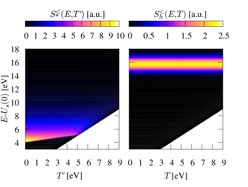
Both source terms are illustrated in Fig. 2 for the parameters given in Table 1, which are used for the numerical calculations described in the next section. The normalization density in the source term for the holes is chosen such that the flux is conserved across the interface. With this source term, holes are injected at the ionization energy of an argon atom, homogeneously distributed in lateral direction. The width accounts for an energy spread in the neutralization process. The source for electrons depends on the reflection coefficient . For a surface potential with the depth of the electron affinity and a tail on the plasma side due to the image charge (Schottky effect), the coefficient becomes, adapting results from Ref. MacColl (1939),
| (16) |
with
| (17) |
where denotes the Whittaker function, its first derivative with respect to ,
| (18) | ||||
| (19) |
and is the complex conjugate of . As can be seen in Fig. 2, due to the high temperature, electrons are injected into the conduction band of the semiconductor over a wide range of energies, with most weight at the low energy cutoff given by .
Since the plasma is treated collisionless, the solutions of the Boltzmann equations on the plasma side are completely determined by the profile of the electric potential and the boundary conditions at and . The latter are given by (13b), where the ions are restricted to energies above the presheath potential , which needs to be determined selfconsistently. It is responsible for the acceleration of ions before reaching the sheath and can be determined from the generalized Bohm criterion Riemann (1991),
| (20) |
In our formalism, it follows from Eq. (2), where the radicand needs to be positive for . As usual, we enforce marginal fulfillment. Thus, is determined by Eq. (20) with the equal sign. In this work, we will prescribe the plasma density . Enforcing Eq. (20) instead of , as in Rasek et al. (2020), is then numerically advantageous.
For the current-voltage characteristic we need the particle fluxes. As for the densities given in Eq. (10), we initially define energy-resolved fluxes,
| (21) |
in terms of which the macroscopic fluxes required for the characteristic become
| (22) |
II.2 Numerical strategy
In the following, we give a sketch of the numerical strategy used for solving the kinetic problem stated in the previous subsection. Due to the changes in the boundary and matching conditions, the strategy differs somewhat from the one used previously Rasek et al. (2020). In particular, the procedure for establishing selfconsistency between the plasma and the solid side of the interface is different due to the reflectivity of the interface. The isotropy of the collision integrals enables us moreover to discretize a much larger energy domain.
Besides the distribution functions and the electric potential profile , three energy parameters , , and and two density parameters and have to be selfconsistently determined for prescribed plasma density and external voltage . The five equations required for it are, the charge neutrality condition at , providing two equations, , the electric matching condition (4), the generalized Bohm criterion (20), and the condition (1) following from the definitions of the potential drops at the interface. The net flux through the interface,
| (23) |
due to flux conservation identical to the flux anywhere in the device, is then obtained as a function of . It will be however numerically advantageous to specify instead of and to initially determine from which follows straight by applying Eq. (1).
For the numerical implementation of the selfconsistent calculation of the current-voltage characteristic we rewrite the Boltzmann equations (6) for the charge carriers inside the semiconductor in integral form (suppressing the parametrical dependencies on and ) Rasek et al. (2020),
| (24a) | |||
| and | |||
| (24b) | |||
with the integrating factor
| (25) |
and .
To avoid the integrable divergences of at , that is, at the turning points for the perpendicular motion, where the charge carriers move parallel to the interface, it is convenient to perform a coordinate transformation from to . Using , , and , we find
| (26a) | ||||
| (26b) | ||||
which enables us to rewrite the integrals as integrals. If the semiconducting layer is not too thick, the electric field is finite in the whole integration domain. Thus, using this substitution we can avoid diverging integrands in the numerical solution of the Boltzmann equations.
After the transformation, the coordinates , , and are discretized, with the discretization kept fixed during the iteration. Through the domain of , we thus prescribe the value , although it is actually a parameter to be determined selfconsistently for given . Instead of , we use as a derived parameter, which allows a better handling of the turning points, where and . Due to Eq. (1) this is permissible.
The remaining four parameters, , , , and are determined from the charge neutrality at , bringing in two equations and yielding in terms of and , the matching condition (4), and the generalized Bohm criterion (20). The latter two provide at the end two coupled equations for and which have to be solved selfconsistently with the Boltzmann equations and the Poisson equation on both sides of the interface.
To get the two equations, we relate the potential drop to by the integral
| (27) |
Inserting from Eq. (3), setting , since we consider in the next section an undoped germanium layer, and solving for yields
| (28) |
that is, the electric field at necessary to produce, with the net charge distribution , the potential drop over the width of the semiconductor.
The electric field , on the other side of the interface, in turn can be obtained from Eq. (2). Inserting the electron and ion densities arising from the electron and ion distribution functions , which can be largely worked out analytically Rasek et al. (2020), we get
| (29) |
with
| (30) | ||||
| (31) | ||||
| (32) |
where we used , because of the choice of the reference point for the potentials, set , and . The symbols and denote the error and complementary error function.
Multiplying Eq. (28) by the dielectric constant and equating it with Eq. (29), an equation is obtained relating to , , and . Since and are external parameters, we thus have a relation between and , as required. For a perfectly absorbing interface .
A second relation between and follows from the generalized Bohm criterion. Expressing again and in terms of the distribution functions , and using the definitions introduced above, we obtain
| (33) |
with
| (34) |
and
| (35) | ||||
| (36) |
where has been used once again. We thus have a second equation connecting and . Note, through Eq. (14d), the electron distribution function on the plasma side depends on the electron distribution function inside the solid, providing an additional feedback of the solid to the plasma, in addition to the electric matching (4). For a perfectly absorbing interface this kind of feedback is absent.
With the parameters and , the particle fluxes and hence the source functions are fixed. Inserted in the boundary conditions (14b) and (14c), the distribution functions for valence band holes and conduction band electrons are obtained from Eqs. (24), with the substitutions (26), from which follow also the densities according to Eq. (11), which in turn can be fed into the Poisson equation (3) to yield a new potential to be used in the next iteration step. For semiconductors with high intrinsic densities, such as germanium, it turns out that the change in densities caused by the injected charge carriers is negligible compared to the Maxwellian background of intrinsic carriers. It is thus possible to neglect it in the source term of the Poisson equation, reducing thereby the calculational costs substantially. The densities plotted in Fig. 5 verify a posteriori the validity of this simplification.
The iteration starts with constant Maxwellian distributions in accordance to the boundary conditions (14), but for conduction band electrons continued to energies which are not accessible at due to the higher value of . Successively, the distribution functions are updated by Eq. (24), as are the parameters and by Eq. (4), expressed in terms of Eqs. (28) and (29), and Eq. (33). In contrast to the perfectly absorbing interface Rasek et al. (2020), the plasma parameters now change slightly in each iteration step, which in turn changes also the matching conditions at the interface. The updating is repeated until convergence is reached. It should be noted that the conduction band electron and valence band hole distribution functions also enter the in-scattering collision integrals in Eqs. (24). Hence, even without the coupling to the plasma and changing boundary conditions, an iteration is required to solve the Boltzmann equations inside the germanium layer. This is also the case when the Grinberg-Luryi approach Grinberg and Luryi (1992) is applied to semiconductor device modeling A. R. St. Denis and D. L. Pulfrey (1998); Konistis and Hu (2002).
III Results
This section discusses the numerical results obtained for an argon plasma in contact with a germanium layer. The material parameters are given in Table 1. We split the discussion into three parts, depending on the perspective from which the device shown in Fig. 1 is analyzed. First, regarding it as part of an electric circuit, we present the current-voltage characteristic in subsection III.1. Then, we proceed to discuss in subsection III.2 the spatial profiles of the electric potential and the species’ densities as well as fluxes. Finally, in subsection III.3, we turn to the energetically and spatially resolved distribution functions of the charge carriers inside the semiconducting layer.
III.1 Electric picture
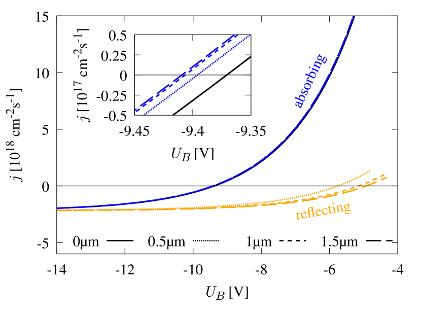
A biased plasma-solid interface can be considered as part of an electric circuit and thus as an electric device characterized by a current-voltage characteristic, that is, the net flux (current density) flowing through the system as a function of the bias voltage . For germanium layers of different thicknesses in contact with an argon plasma, the characteristics are shown in Fig. 3.
The germanium layers are terminated by an Ohmic contact, which is not further characterized in the model. It merely acts as a sink for any flux carrying particles reaching the semiconductor-metal interface. For , that is, without the semiconducting layer, the system is thus a perfectly electron absorbing Langmuir probe Mott-Smith and Langmuir (1926); Cherrington (1982); Lam (1965). Current-voltage characteristics are given for different thicknesses of the germanium layer, for both the electron reflecting and the perfectly absorbing semiconductor-plasma interface. In the latter, the matching conditions (14c) and (14d) are replaced by the assumption that every electron impinging on the interface from the plasma is absorbed by the germanium layer and every electron reaching the interface from the inside of the layer is specularly reflected. The boundary conditions then take a form similar to Eqs. (14a) and (14b), with the injection term (15b) normalized such that the electron flux is conserved across the interface.
Within the perfect absorber model, there are hardly any differences in the current-voltage characteristics of the Ohmic and the semiconducting plasma-solid interface (black and blue lines in Fig. 3). The characteristics of the latter are only shifted to lower voltages because of the voltage drops inside the semiconductor, as can be seen in the inset of the figure for different film thicknesses. The shifts are a few tens of mV, with a thicker layer giving rise to a larger shift. If the layers were thick enough to host the whole negative space charge, the shifts would saturate, because of the vanishing electric field deep inside the semiconductor. For the thicknesses shown in Figs. 3 this is however not yet the case. Since, as discussed in the next paragraph, the voltage drops across reflecting and absorbing germanium layers of the same thickness turn out to be essentially identical, because and are rather small, and hence effectively negligible in Eq. (33), the large shift between the blue and orange lines visible in the main panel is a consequence of the reflected and emitted electron fluxes, which can be rather significant. From a broader perspective, the results shown in Fig. 3 imply that modifications of the surface of a Langmuir probe, for instance, by an oxide film, affects the current-voltage characteristic only by a small amount if the perfect absorber assumption holds. However, if this is not the case, the characteristic depends on the film. In particular, the zero-crossing, that is, the floating potential, would depend strongly on the emissive properties of the film.
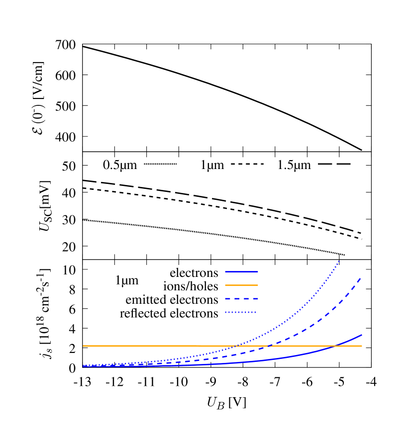
To gain more insights, we plot in Fig. 4, as a function of the bias voltage , the electric field at the interface, the potential drop across the semiconducting layer, and the electron and hole fluxes. The electric field at the interface is independent of the thickness of the layers, only the potential drop depends on it. The fluxes are shown representatively only for a thick semiconducting layer, with electron fluxes split into the contributions arising from electrons reflected at the potential step and electrons emitted from the semiconductor, that is, electrons which made it into the layer but are backscattered by electron-phonon collisions inside it. The two contributions arise, respectively, from the first and second term of Eq. (14d).
While the reflected flux is independent of the thickness of the layer, since it only depends on the reflection coefficient , the emitted flux increases with the thickness of the layer, leading to smaller total net fluxes towards the Ohmic contact, as can be also seen in Fig. 3. This may be an artifact of the simple model we employ for the germanium layer. Flux-carrying electrons, having typically large energy, as we will see in subsection III.3, undergo in this model only a few collisions while passing through the layer. The thicker the layer, the higher is thus the chance of an electron belonging to this group for being backscattered. Hence, the emitted flux increases with layer thickness.
The electron fluxes decay exponentially the more negative the bias voltage is, since the fraction of the Maxwellian distribution of plasma electrons contributing to the flux by overcoming the sheath potential decreases. Only few electrons in its high energy tail contribute to the flux across the interface and have thus a chance to get reflected or emitted. The emitted and reflected electrons, encoded in and , modify thus (33) only weakly and are hence negligible, as it is also the case in the source term of the Poisson equation, where emitted and reflected electrons are dominated by the plasma electrons belonging to the low energy part of the Maxwellian.
III.2 Macroscopic picture
Besides regarding the interface as an electric device, characterized by a current-voltage characteristic, it is also instructive to consider it as a system of charged particles, characterized by density, flux, and potential profiles. We limit the discussion in this and the next subsection to the reflecting interface at the floating point, where the electron and ion/hole fluxes are equal, noting, however, that for different bias voltages the fundamental observations are similar, differing only by the numerical values.
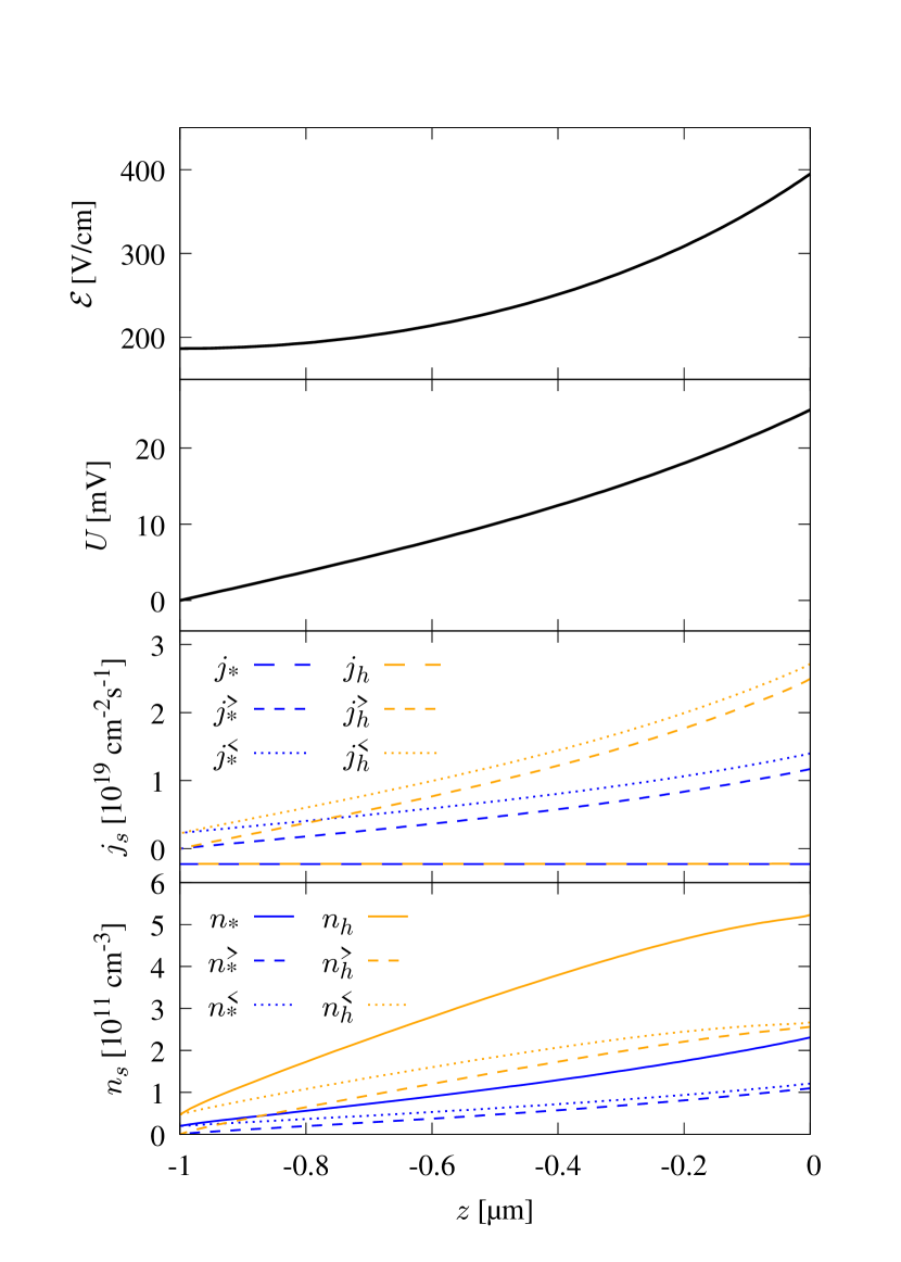
Figure 5 shows from top to bottom the spatial profiles for the electric field, the electric potential, the fluxes, and the densities of the injected carriers for an interface with a thick germanium layer. As it was the case on the plasma side, the injected carriers, for which we show the fluxes and densities, are also negligible in the source term of the Poisson equation on the solid side of the interface. The solid-bound parts of the electric field and potential shown in the top two panels are thus determined by the intrinsic charge carriers. Hence, the solid-bound part of the electric double layer plotted in the inset of the top panel, is the result of the selfconsistent distribution of the intrinsic charge carriers in the electric field arising due to the interface. For germanium, the intrinsic density at room temperature is , and thus much larger than the net density of the injected carriers, which, according to the bottom panel of Fig. 5, is even at only only around , and hence about two orders of magnitude smaller. The simplification we made for the solution of the Poisson equation is thus valid. It not only stabilizes the iteration process, but allows also for an efficient implementation, which reduces the computation time by about two orders of magnitude.
The electric potential, shown in the second panel from the top of Fig. 5, is shifted such that . The potential drop across the germanium layer meV can thus be read off directly at . It can be also immediately seen that the electric field is the derivative of the electric potential. The fluxes, finally, are shown in the third panel from the top. In addition to the net fluxes, and , which are conserved and hence independent of , left- and right-moving fluxes are also plotted. They decay exponentially with decreasing . The net flux is the difference of the right- and left-moving fluxes. It is negative, showing that more electrons and holes are moving towards the Ohmic contact than in the other direction. The conservation of the net flux is a consequence of the modeling of the germanium layer, which contains only particle-conserving collisions with phonons. Had we incorporated also particle non-conserving scattering processes, such as radiative and non-radiative electron-hole recombination or impact ionization, the net fluxes of each species would not be conserved. However, to have flux conservation as an important indicator of the numerical accuracy of the implementation of the selfconsistency scheme (it is not explicitly kept constant in the iteration scheme), we neglected in this exploratory work particle non-conserving scattering processes.
III.3 Microscopic picture
We now turn to the microscopic picture as it arises from the distribution functions satisfying the two coupled sets of Boltzmann-Poisson equations. The electric and macroscopic pictures contain this information only in an integral manner. Now, we take an energy-resolved look at the kinetics of the charge carriers across the interface. The dependence of the distribution functions on the total energy and the lateral kinetic energy enables us to visualize energy relaxation due to collisions with phonons as well as the motion of the charge carriers parallel to the interface.
Let us first look at the energy-resolved net fluxes per species defined in Eq. (21). For an interface with a thick germanium layer at the floating point, the fluxes flowing from the plasma towards the Ohmic contact are plotted in Fig. 6. On the left (right), fluxes inside the germanium layer (plasma) are shown. While the species’ energy-integrated net fluxes are constant, the energy-resolved net fluxes display a rich behavior along the germanium layer.
The net electron flux approaching the interface from the plasma side splits inside the solid into a high- and a low-energy component. The former comprises electrons remaining close to the energy where they have been initially injected. Because the germanium layer is rather thin, a large number of electrons reaching the Ohmic contact suffer only a few electron-phonon collisions. Hence, they loose only a small amount of energy and remain energetically high in the conduction band. Yet, some electrons scatter often enough to end up at the band minimum. There is thus also a net flux at low energy. In absolute numbers, this is even larger than the one at high energies (note the different scales for high and low energies). However, its contribution to the macroscopic net flux is rather small because the energy range over which it is integrated is rather narrow. The main contribution to the net total electron flux arises thus from high-energy electrons. In numbers, we find of the total electron flux to be carried by the hot electrons, with energies above , and only by the low energy electrons.
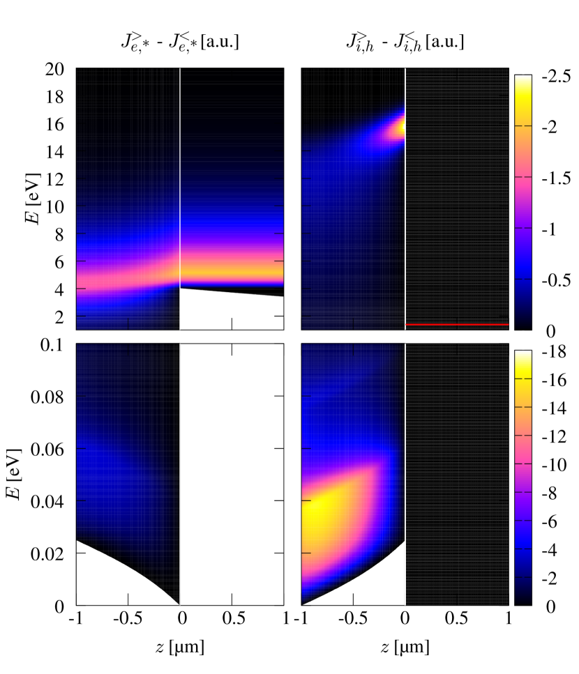
The net flux of valence band holes, arising from the neutralization of ions, hitting the interface with thermal kinetic energy, shows qualitatively the same behavior. Holes, injected high up in the valence band at , relax due to collisions with phonons to the bottom of the band. Quantitatively, however, the situation is different. Due to the larger effective mass, holes loose energy due to collisions with phonons more efficiently than electrons. The scattering rate , for instance, defined in Eq. (8), is proportional to . Hence, it increases with the effective mass. The same holds for the in-scattering parts of the collision integral . Thus, the larger the effective mass of the charge carriers, the smaller is the inelastic mean free path, and hence the spatial scale required to loose a substantial amount of energy. The thick germanium layer provides apparently enough space for a significant number of holes to relax to the bottom of the band and to give rise to a rather pronounced hole flux at low-energies. Integrated over energy, the low-energy flux provides about to the total net flux. The high-energy flux is hence still dominant but not as dominant as in the case of electrons.
Energy relaxation of electrons and holes stops when their energies, measured from the bottom of the conduction and valence band, respectively, are less then the phonon energy. There is thus a threshold for energy relaxation, leading to a kind of energy backlog in the fluxes up to a phonon energy above the band minima. By absorbing phonons, carriers caught in the backlog can reach higher energies. For holes, this is clearly visible in Fig. 5. It leads to the feature in the bottom right panel around , which is roughly twice the phonon energy. After the injected holes emitted several hundred phonons, each carrying away eV, their energies fall below the threshold. Collisions are then less frequent, as the emission (second) term in the scattering rate (8) disappears. The relatively high population of the holes just below the phonon energy makes however the absorption process operative in the collision integrals leading to the feature in the hole flux around twice the phonon energy.
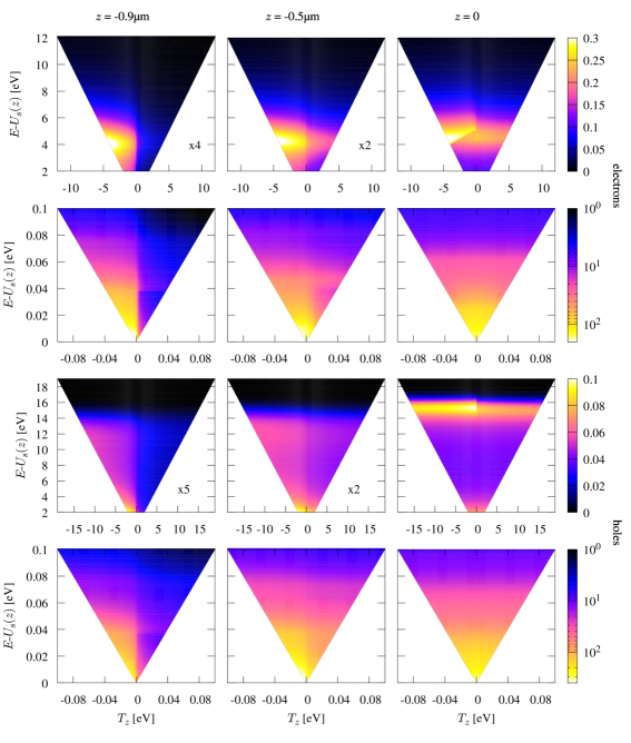
Finally, we discuss for the thick germanium layer the distribution functions . In addition to the effects already present in the energy-resolved net fluxes, there are now also features due to the lateral motion of the charge carriers. The distribution functions are plotted in Fig. 7, with the two top (bottom) rows showing the data for conduction band electrons (valence band holes). Three spatial locations are considered and data for high and low energies are plotted in separate panels. The lateral coordinate of the plots encodes by its sign also the direction of motion, and is chosen such, that for it describes the turning points. Note the linear scale for high and the logarithmic scale for low energies. As for the macroscopic densities plotted in Fig. 5, the Maxwellian background of intrinsic carriers is not included in the data. Only the distribution functions for the surplus electrons and holes arising from the plasma are shown.
In the high energy parts of the distribution functions right at the interface, at (right column), the source functions and , describing the injection of electrons and holes, can be clearly identified. Due to the collisions with phonons there is also a noticeable portion of right-moving charge carriers, as can be seen from the rather large numerical values for . For electrons, this group of charge carriers eventually leads to the flux of emitted electrons, if they also make it through the potential barrier, and hence to secondary electron emission. As a consequence of energy relaxation, Maxwellian distributions are established for both species at low energies. Indeed, the low-energy parts of the distribution functions are rather homogeneous in the lateral direction and exponentially decaying with total energy, as it should be for Maxwellians. As a consequence of the Maxwellian distribution at low energies, there is no low-energy flux present at , in accordance with the data shown in Fig. 6.
In the center of the germanium layer, at m (center column), the sharp features of the source functions are softened due to collisions with phonons. A surplus motion to the left is also building up, most distinctly for conduction band electrons, and weaker for valence band holes. At low energies, the surplus of left-moving charge carriers remains, but it is now somewhat more dominant for holes. Due to the imbalances, the distribution functions at low energy start to deviate from Maxwellian distributions. As a result, low-energy fluxes are building up, as can be also seen in Fig. 6. The behavior of the energy-resolved net fluxes can thus be explained by the changes in the distribution functions caused by the scattering processes.
The distribution functions at m (left column), finally, are already dominated by the boundary condition , set for the injected carriers at the interface to the Ohmic contact. For both species, the motion is heavily biased to the left, irrespective of the energy. While right-moving electrons and holes are strongly suppressed, there is a faint feature in and slightly above the phonon energy which arises from collisions with phonons. The features of the source functions are still visible in the high-energy parts of and , albeit severely washed out, and at low energies and remain Maxwellian. It should be noted that at high energies the absolute values of the distribution functions decay with approaching . The ratio, however, of left to right moving distributions grows. Hence, the net flux at high energies stays high, even though the individual distribution functions for left- and right-moving carriers decay with decreasing , just like the direction-resolved fluxes shown in Fig. 5.
IV Conclusion
We presented a kinetic description of ambipolar charge transport across a biased plasma-solid interface consisting of a semiconducting germanium layer sandwiched between an argon plasma and an Ohmic contact. The electron-hole plasma within the semiconductor is coupled to the electron-ion plasma in front of it through matching conditions for the distribution functions and the electric field at the interface. Argon ions impinging on the germanium layer create holes in the valence band, whereas electrons may be quantum-mechanically reflected or transmitted. Electrons entering the semiconductor from the plasma may be emitted back to it due to collisions with phonons inside the solid, which also cause energy relaxation in its valence and conduction band. To drive a current through the setup, a bias voltage is applied between the bulk of the argon plasma, which we provide with a prescribed plasma density, and the Ohmic contact used to collect the current.
From the distribution functions for the charge carriers on both sides of the interface, we calculated the current-voltage characteristic. Due to the quantum-mechanical reflection at the plasma-solid interface and the collisions inside the solid, the characteristic differs significantly from the one obtained for an interface which absorbs electrons from the plasma perfectly and keeps them in the solid forever. Hence, the electron microphysics of the semiconductor affects the electric properties of the interface and should thus be considered by its theoretical description as well as its experimental analysis.
We focused in this work on the implementation of a numerical scheme for the selfconsistent calculation of the distribution functions and potential profiles building up at the flux-carrying plasma-solid interface. For that purpose, we kept the argon plasma collisionless and allowed electrons and holes inside the germanium layer to scatter only on phonons. Particle nonconserving collisions are not included. Within the simplified model, we find flux-carrying conduction band electrons to remain at the high energies set by the injection process. Due to the boundary and matching conditions, the surplus electrons inside the semiconductor are thus rather hot and not in thermal equilibrium with the intrinsic electrons. The same holds for injected holes. With increasing layer thickness, we find secondary electron emission, encoded in the emitted electron flux, to increase because a surplus electron is then more likely to suffer collisions with phonons, which may bring it back to the plasma, if it also successfully traverses the potential step at the plasma-solid interface. The selfconsistent distribution functions enable us, moreover, to visualize how the ambipolar gaseous charge transport in the argon plasma merges with the solid-bound ambipolar charge transport inside the germanium layer.
Albeit the description of the argon plasma is also somewhat crude, containing an unspecified source and a collisionless sheath made consistent with the germanium layer due to an equally unspecified presheath, the idealized electronic structure of the germanium layer is more limiting. A quantitative modeling of the biased plasma-solid interface has to be based on a realistic band structure of the plasma-facing semiconductor. It should contain, over the energy range set by the injection processes, the electronic structure of the surface, entering the calculation of the electron reflectivity and the modeling of the hole source function, as well as the electronic structure of the bulk, which enters the collision integrals of the Boltzmann equations and determines the velocity of the charge carriers. Of particular importance are Bragg gaps preventing the transmission of electrons across the interface and surface states trapping electrons and/or holes close to it. Since the injection of electrons and holes occurs at rather high energies, impact ionization, creating electron-hole pairs across the band gap, and its inverse, the recombination of electron-hole pairs have to be moreover also included in a modeling which attempts to provide more information than the insight that current-carrying conduction band electrons and valence band holes are rather hot.
Acknowledgments
Support by the Deutsche Forschungsgemeinschaft through project BR-1994/3-1 is greatly acknowledged.
References
- Franklin (1976) R. N. Franklin, Plasma Phenomena in Gas Discharges (Clarendon Press, Oxford, 1976).
- Lieberman and Lichtenberg (2005) M. A. Lieberman and A. J. Lichtenberg, Principles of Plasma Discharges and Materials Processing (Wiley-Interscience, New York, 2005).
- Langmuir and Mott-Smith (1924) I. Langmuir and H. Mott-Smith, Gen. Electr. Rev. 27, 449 (1924).
- Nemschokmichal et al. (2018) S. Nemschokmichal, R. Tschiersch, H. Höft, R. Wild, M. Bogaczyk, M. M. Becker, D. Loffhagen, L. Stollenwerk, M. Kettlitz, R. Brandenburg, and J. Meichsner, Eur. Phys. J. D 72, 89 (2018).
- Peeters et al. (2016) F. J. J. Peeters, R. F. Rumphorst, and M. C. M. van de Sanden, Plasma Sources Sci. Technol. 25, 03LT03 (2016).
- Wagner et al. (2005) H.-E. Wagner, Y. V. Yurgelenas, and R. Brandenburg, Plasma Phys. Control. Fusion 47, B641 (2005).
- Massines et al. (2003) F. Massines, P. Segur, N. Gherardi, C. Khamphan, and A. Ricard, Surface and Coatings Technology 174-175, 8 (2003).
- Kogelschatz (2003) U. Kogelschatz, Plasma Chem. and Plasma Proc. 23, 1 (2003).
- Chiang et al. (2019) W.-H. Chiang, D. Mariotti, R. M. Sankaran, J. G. Eden, and K. Ostrikov, Adv. Materials 2019, 1905508 (2019).
- Eden et al. (2013) J. G. Eden, S.-J. Park, J. H. Cho, M. H. Kim, T. J. Houlahan, B. Li, E. S. Kim, T. L. Kim, S. K. Lee, K. S. Kim, J. K. Yoon, S. H. Sung, P. Sun, C. M. Herring, and C. J. Wagner, IEEE Trans. Plasma Science 41, 661 (2013).
- P. A. Tchertchian, C. J. Wagner, T. J. Houlahan Jr., B. Li, D. J. Sievers, and J. G. Eden (2011) P. A. Tchertchian, C. J. Wagner, T. J. Houlahan Jr., B. Li, D. J. Sievers, and J. G. Eden, Contr. Plasma Phys. 51, 889 (2011).
- Dussart et al. (2010) R. Dussart, L. J. Overzet, P. Lefaucheux, T. Dufour, M. Kulsreshath, M. A. Mandra, T. Tillocher, O. Aubry, S. Dozias, P. Ranson, J. B. Lee, and M. Goeckner, Eur. Phys. J. D 60, 601 (2010).
- Bronold and Fehske (2017) F. X. Bronold and H. Fehske, J. Phys. D: Appl. Phys. 50, 294003 (2017).
- Schwager and Birdsall (1990) L. A. Schwager and C. K. Birdsall, Phys. Fluids B 2, 1057 (1990).
- Riemann (1991) K. U. Riemann, J. Phys. D: Appl. Phys. 24, 493 (1991).
- Franklin (2003) R. N. Franklin, J. Phys. D: Appl. Phys. 36, R309 (2003).
- Brinkmann (2009) R. P. Brinkmann, J. Phys. D: Appl. Phys. 42, 194009 (2009).
- Robertson (2013) S. Robertson, Plasma Phys. Control. Fusion 55, 093001 (2013).
- Rasek et al. (2020) K. Rasek, F. X. Bronold, and H. Fehske, Phys. Rev. E 102, 023206 (2020).
- Mott-Smith and Langmuir (1926) H. M. Mott-Smith and I. Langmuir, Phys. Rev. 28, 727 (1926).
- Cherrington (1982) B. E. Cherrington, Plasma Chem. and Plasma Proc. 2, 113 (1982).
- Lam (1965) S. H. Lam, Phys. Fluids 8, 73 (1965).
- Jacoboni and Reggiani (1983) C. Jacoboni and L. Reggiani, Rev. Mod. Phys. 55, 645 (1983).
- Ridley (1999) B. K. Ridley, Quantum Processes in Semiconductors (Clarendon Press, Oxford, 1999).
- Roth (1992) L. Roth, in Handbook on Semiconductors, edited by T. S. Moss (Elsevier Science Publishers B. V., Amsterdam, NL, 1992) p. 489.
- Grinberg and Luryi (1992) A. A. Grinberg and S. Luryi, Solid-St. Electron. 35, 1299 (1992).
- Moglestue (1993) C. Moglestue, Monte Carlo Simulation of Semiconductor Devices (Chapman & Hall, London, 1993).
- MacColl (1939) L. A. MacColl, Phys. Rev. 56, 699 (1939).
- A. R. St. Denis and D. L. Pulfrey (1998) A. R. St. Denis and D. L. Pulfrey, J. Appl. Phys. 84, 4959 (1998).
- Konistis and Hu (2002) K. Konistis and Q. Hu, J. Appl. Phys. 91, 5400 (2002).