single=false \DeclareAcronymfmshort = FM, long = ferromagnet, short-indefinite =an, long-indefinite =a \DeclareAcronymafmshort = AFM, long = antiferromagnet, short-indefinite =an, long-indefinite =an \DeclareAcronymdmishort = DMI, long = Dzyaloshinskii–Moriya interaction \DeclareAcronymsocshort = SOC, long = spin-orbit coupling \DeclareAcronymnsotshort = NSOT, long = Néel-spin-orbit torques, short-indefinite =an, long-indefinite =a \DeclareAcronymllgshort = LLG, long = Landau–Lifshitz–Gilbert, short-indefinite =an, long-indefinite =a \DeclareAcronymskkrshort = SKKR, long = screened Korringa–Kohn–Rostoker, short-indefinite =an, long-indefinite =a \DeclareAcronymscfshort = SCF, long = self-consistent field, short-indefinite =an, long-indefinite =a \DeclareAcronymrspshort = RSP, long = relativistic spin-polarized, short-indefinite =an, long-indefinite =a \DeclareAcronymrtmshort = RTM, long = Relativistic Torque Method, short-indefinite =an, long-indefinite =a \DeclareAcronymasashort = ASA, long = atomic sphere approximation \DeclareAcronymdlmshort = DLM, long = Disordered Local Moment \DeclareAcronymrdlmshort = RDLM, long = relativistic Disordered Local Moment \DeclareAcronymsceshort = SCE, long = Spin-Cluster Expansion \DeclareAcronymdosshort = DOS, long = density of states
Current induced switching in \ceMn2Au from first principles
Abstract
It is well established that it is possible to switch certain antiferromagnets electrically, yet the interplay of \acnsot and thermal activation is only poorly understood. Combining ab initio calculations and atomistic spin dynamics simulations we develop a multiscale model to study the current induced switching in \ceMn2Au. We compute from first principles the strength and direction of the electrically induced magnetic moments, caused by the Rashba–Edelstein effect, and take these into account in atomistic spin dynamics simulations. Our simulations reveal the switching paths as well as the time scales for switching. The size of the induced moments, however, turns out to be insufficient to lead to fully deterministic switching. Instead, we find that a certain degree of thermal activation is required to help overcoming the relevant energy barrier.
I Introduction
afm are promising materials for spintronic devices. Among the advantages over \acpfm are the lack of stray fields, the very low susceptibility to magnetic fields, the abundance of materials and much faster spin dynamics [1, 2, 3]. However, the antiferromagnetic order parameter in \acpafm is difficult to read and to control because of a lack of macroscopic magnetization, a fact which is strongly related to some of their advantages. A major step in the field of antiferromagnetic spintronics [1, 2, 3] was the discovery of electrically induced \acnsot [4, 5, 6, 7, 8] in specific antiferromagnetic materials. These torques are a result of a special magnetic structure, where, for the magnetic state, global inversion symmetry is broken but one sublattice forms the inversion partner of the other, in combination with the inverse spin-galvanic or (Rashba–)Edelstein effect [4], which is the generation of a nonequilibrium spin polarization by electrical currents. Currently, \ceCuMnAs and \ceMn2Au are the two known materials that provide antiferromagnetic order at room temperature and possess the specific crystal structure required for \acnsot. The latter is the more promising material as its critical temperature is extremely high—higher than the peritectic temperature of about , where the material decomposes [9]—and it is easier to handle due to the lack of toxic components.
Despite the fact that several studies clearly demonstrate that it is possible to switch the order parameter of \ceMn2Au via the application of an electrical current by [4, 10, 11, 7, 12], the switching mechanism—whether deterministic or thermally activated, coherent or via domain wall motion—remains concealed. The employed models and simulations so far rest on phenomenological descriptions [10] and macrospin approximations [11]. A microscopic and quantitative model of the switching process is missing.
Here, we combine ab initio calculations with atomistic spin dynamics simulations to develop and employ a multi-scale model of the current induced switching in \ceMn2Au. The three ingredients for this multi-scale model are ab initio calculations of the exchange interactions and anisotropies (section II), first-principles calculations of the current induced magnetic moments (section III), and atomistic spin model simulations (section IV), that include the results from the first-principles calculations and investigate the switching mechanism and its dynamics. We show that the switching is fast, on a time scale of some tens of picoseconds, but not purely deterministic, requiring some degree of thermal activation to overcome the anisotropy energy barrier during the switching process.
II Derivation of the spin model from ab initio calculations
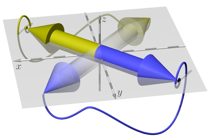
We employ the fully relativistic \acskkr method [13] to determine the electronic structure and magnetic interactions of \ceMn2Au. \ceMn2Au crystallizes in the \ceMoSi2 structure with the lattice constants and [14, 15, 9]. The \ceMoSi2-type lattice geometry is depicted in Fig. 1. The potentials were treated within the \acasa with an angular momentum cutoff of to describe the electron scattering. For energy integrations we used 15 energy points on a semicircular contour on the upper complex semiplane, and up to 7260 -points in the irreducible wedge of the Brillouin zone near the Fermi energy for the calculation of spin model parameters.
We perform self-consistent calculations for the layered \acafm state shown in Fig. 1, which has been identified as the magnetic ground state by neutron diffraction experiments [9], but also for the \acfm state. We find the layered \acafm state lower in energy than the \acfm state by 25.8 mRy/atom, which compares fairly well to the value reported in Ref. [16] (21.5 mRy/atom). Also in agreement with Ref. [16] we obtain a larger magnetic moment for the \ceMn atoms in the layered \acafm state () than in the \acfm state (). For the description of the switching process we consider the following spin model:
| (1) | ||||
where the isotropic exchange interactions are obtained from the \acrtm [17], while the anisotropy parameters , and are derived from band energy calculations in the spirit of the magnetic force theorem [18].
The isotropic exchange interactions calculated from the layered \acafm state as reference are plotted in Fig. 1 as a function of the interatomic distance. We can identify three dominant Heisenberg couplings: antiferromagnetic ones for the two nearest neighbors, and , but a ferromagnetic one for the third nearest neighbor, . These values show good qualitative agreement with those calculated in Ref. [16] also in terms of the KKR-ASA method, but using a cutoff of for the partial waves, , and . Since the interactions and act between sublattices (layers), while is the leading interaction within a sublattice (cf. Fig. 1), these couplings clearly favor the layered \acafm state as the ground state of the system.
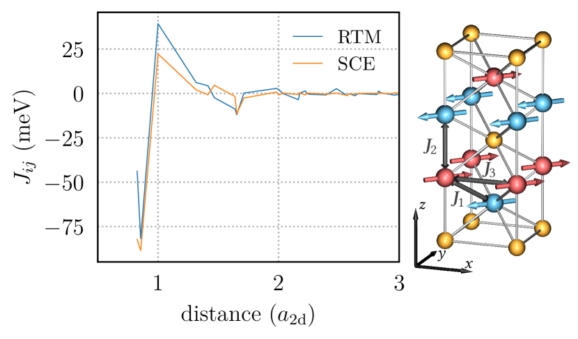
It turns out that taking into account only the first three nearest neighbor interactions is not sufficient for a precise determination of the inter- and intra-sublattice interactions. In our simulations we, hence, consider interactions up to a distance of , resulting in an inter-sublattice exchange interaction of and an intra-sublattice exchange interaction of . Considering exchange interactions only in the first three shells yields and , being thus 30 and 14 % smaller in magnitude than the ones calculated with a spatial cutoff of .
Experimental values for the effective inter-sublattice exchange coupling, [19], were previously provided based on susceptibility measurements for \ceMn2Au powder [9] and thin films [19], and , respectively. The corresponding values from our calculations, , and the one derived from the exchange interactions in Ref. 16, , compare remarkably well and are also in good agreement with the experimental result for the powder sample [9].
From our spin dynamics simulations we obtain a Néel temperature of , which is in good agreement with the value of calculated in Ref. [16] via Monte-Carlo simulations using nine nearest neighbor shells (the numerical values of which, however, were not provided beyond the first three shells). Note that due to a peritectic temperature of , the Néel temperature can only be extrapolated from experiments, yielding values in the range of [9].
In order to support the validity of our spin model description relying on the assumption of rigid magnetic moments that are stable against magnetic disorder, we also perform calculations using the \acrdlm theory [20, 21]. This approach assumes a fully spin disordered reference state, and also enables the extraction of spin model parameters by means of the so-called \acsce [22, 23], which maps the adiabatic magnetic energy surface onto a spin model.
The resulting isotropic Heisenberg couplings are also displayed in Fig. 1. There is a remarkable similarity between the two spin model parameter sets, despite their quantitative differences especially for the first and third neighbor shells. Obviously, the interactions obtained from the \acsce-\acrdlm calculation are also consistent with the layered \acafm structure as ground state and we obtain a Néel temperature of , which is in good agreement with the \acrtm.
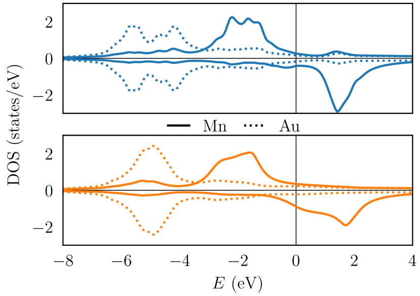
Conceptually, the \acrtm gives a good approximation near the ground state, whereas the \acsce corresponds to a high-temperature phase. The fact that the two sets of parameters agree well despite this fundamental difference between the two methods can be explained by the rigidity of the \ceMn local spin moments. In order to support this point we compare the \acdos for the two magnetic states in Fig. 2. As also noted in Ref. [16], the narrow bandwidth of the \ceMn -bands and the formation of a pseudogap around the Fermi level are visible in the \acafm state. The expected smearing of the \acdos in the \acdlm state due to spin disorder is clearly seen in the bottom panel of Fig. 2, but the large exchange splitting between the two spin channels prevails. This shows up also in the spin moment of \ceMn calculated in the \acdlm state of being practically the same as in the layered AFM state.
As for the anisotropies in Eq. (1), we calculate a second order anisotropy of , and fourth order anisotropies and . These values compare fairly well to those that can be derived from the anisotropy constants reported in Ref. [15], , , and , in particular considering that the latter ones were calculated in terms of a full-potential density functional method contrary to the \acasa we used in our calculations. This result is also in agreement with experimental reports of an upper bound for the in-plane anisotropy of [24]. Thus, in agreement with Refs. [15, 25, 24] we find the magnetic easy axis along the direction as illustrated in Fig. 1. However, in our results the anisotropy responsible for the confinement in the basal plane is only about half in magnitude as compared to Ref. [15]. Note though that the out-of-plane anisotropy plays only a minor role in the switching process discussed in our work.
For our atomistic spin dynamics simulations we combine these anisotropies with the \acrtm exchange parameters since both are calculated from the same converged potential in contrast to the \acsce exchange parameters.
III First-principles calculations of the induced moments
The inverse spin-galvanic or Rashba–Edelstein effect leads to electrically induced magnetic moments. These induced spin and orbital polarizations can be computed using the Kubo linear-response formalism. Specifically, the locally induced polarizations can be expressed as
| (2) |
with and the spin and orbital Rashba–Edelstein susceptibility tensors, respectively, and the applied electric field. The magneto-electric susceptibility tensors can be obtained by evaluating the response to a perturbing electric field, where is the electron charge.
Employing DFT-based single-electron states, the susceptibility tensors are given by [26]
| (3) |
Here, , with the unperturbed relativistic Kohn–Sham single electron energies, is the Brillouin zone volume, is the matrix element of the component of the momentum-operator, and is the occupation of Kohn–Sham state . stands for a matrix element of the spin or orbital angular momentum operator, i.e., for and for . The parameters and are the electronic lifetimes for inter- and intraband scattering processes, respectively. These parameters capture the decay of an electron state due to electron-electron scattering and interactions with external baths, e.g., phonons and defect scattering. In this work, we use an effective decay .
To compute the current induced spin and orbital polarizations on the individual atoms in \ceMn2Au we employ the relativistic DFT package WIEN2k [27], which gives the Kohn–Sham energies and wave functions that are then used in Eq. (III). We calculate the induced magnetic moments for different orientations of the electrical field with respect to the magnetic easy axes, as reversible switching was reported for both the [110] and [100] directions [7]. Furthermore, we evaluate both the induced spin and orbital polarizations. The local magnetic moments induced by the electric field are finally given as .
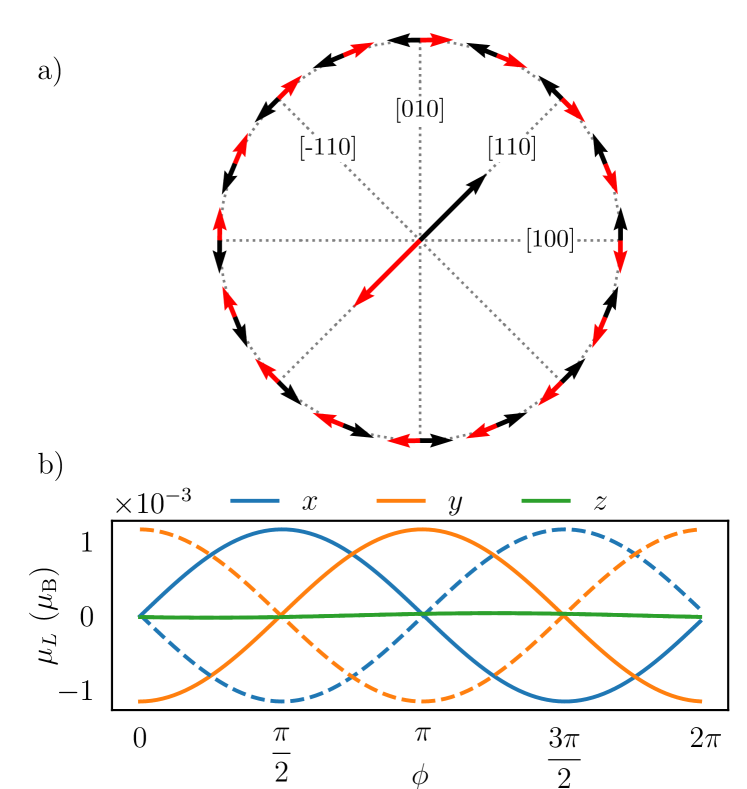
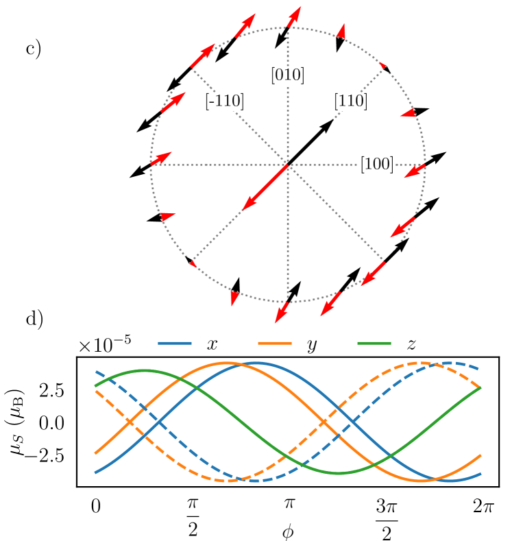
The calculated induced orbital and spin magnetic moments on the two \ceMn sublattices are presented in Fig. 3 as a function of the electric field direction. The orbital moments are always induced perpendicular to the electric field direction and are antisymmetric (staggered) for the \ceMn atoms of two sublattices. The spin moments , on the other hand, are not necessarily perpendicular to the electric field direction, but their in-plane components are staggered as well. Additionally, the spin moments display a homogeneous out-of-plane component, i.e., a non-Néel-type contribution.
Interestingly, in all configurations the induced orbital moments are more than one order of magnitude larger than the induced spin moments, yet the former were not included in previous studies [4, 28]. To summarize, there are always quite large staggered orbital moments induced on the \ceMn sublattices and small induced spin moments with nonstaggered as well as staggered components that can be parallel on antiparallel to the orbital moments depending on the direction of the electric field, see also [12].
IV Atomistic spin dynamics simulations
To include our first-principles calculations in a spin dynamics simulation we extend the semi-classical Heisenberg Hamiltonian [Eq. (1)] by contributions from induced spin and orbital moments,
| (4) | ||||
where is the local magnetic moment of the -electrons, the induced magnetic moment from the conduction -electrons and the induced orbital magnetic moment. All magnetic moments are normalized with respect to the local magnetic moment. Thus, the Hamiltonian consists of five different contributions: the inter-atomic exchange with exchange constant , an additional intra-atomic -exchange with exchange constant , a \acsoc term with strength , as well as second and fourth order anisotropy terms constituting the tetragonal anisotropy.
As our classical spin model employs quantum mechanical and statistical averages of the spin and orbital moments, we also use a classical description of the \acsoc replacing the spin and orbital momentum operators by their averages. Note that this effective model for the \acsoc was used by Bruno [29] in order to provide a simple physical interpretation of magnetic anisotropy. In this model only the spin moments couple via the inter-atomic exchange interaction, which is in agreement with the conclusions from [19].
All the contributions from the induced moments can also be represented by a simple Zeeman-like term with a sublattice-specific effective field that represents the staggered field, which was used in previous phenomenological descriptions,
| (5) |
For the intra-atomic exchange we estimate from the shift in the up and down s-states . The \acsoc strength is calculated from the energy difference between the and resonances yielding . Together with the exchange interactions derived in Sec. II and the induced moment calculated for an electrical field of , this yields staggered fields of about . Here, the contribution from the induced orbital moments dominates [12]. It is about a factor of five larger than the contribution from the inter-atomic exchange and more than one order of magnitude larger than that of the intra-atomic exchange. This explains also why the staggered fields calculated here are much larger than those estimated and predicted before [10, 28, 11] as the orbital contribution was previously not taken into account.
The time evolution of the localized \ceMn moments stemming from the -electrons is described by the stochastic \acllg equation
| (6) |
where is the gyromagnetic ratio and a dimensionless damping constant. Temperature is included via Langevin dynamics by adding a random thermal noise to the effective field [30]. The field from the induced moments is part of this effective field.
The damping constant is a free parameter as there are no experimental values for it in the literature. For comparison with [10] we use a plausible value of . Similar, for the electrical field a rectangular pulse with pulse length of was simulated to compare the results with those from a phenomenological model [10]. Since the samples in experiments are mostly of granular type [11], we simulate a system of size with open boundary conditions, resembling one grain of a typical sample.
In our simulations we consider electrical fields along [110], i.e. parallel to the local magnetic moments, and along [100], since reversible switching was reported for both directions [7]. For both field configurations our model does not switch at for corresponding to currents of about , which are used in experiments [7, 31]. Instead, we need a field strength of at least for the field along the [110] direction, where torques on the local magnetic moments are maximal. For the [100] direction an even larger field of is required for switching at zero temperature. However, once the system switches, it switches within a few picoseconds, see Fig. 4. This is even faster than predicted in the phenomenological model in Ref. [10], probably because of the inclusion of the orbital induced moments and the exchange interactions beyond the first three nearest neighbors.
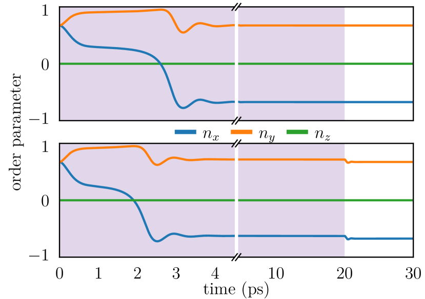
As was already pointed out in Ref. [10], the reason for this rapid switching is the so-called exchange enhancement, which is characteristic for antiferromagnetic dynamics [32]. The staggered fields do not only rotate the magnetic moments via the damping term in the \acllg but also induce a canting between the sublattices via the much stronger precession term. This leads to a very small magnetization resulting in huge torques due to the inter-sublattice exchange field, which tries to realign the sublattices. Here, the damping term is responsible for the realignment. The precession term, on the other hand, rotates the magnetic moments towards the direction of the staggered field. The out-of-plane component of the order parameter remains zero during the process (see Fig. 5). Hence, the inter-sublattice exchange field governs the switching process and, in contrast to the switching in \acpfm, lower damping allows for faster switching [33].
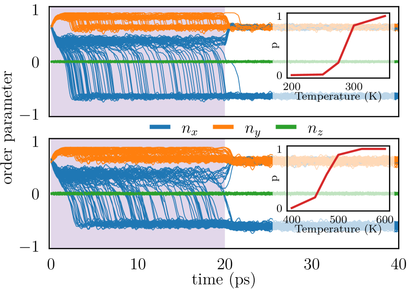
The electric fields considered so far are much larger than those applied in experiments, but temperature plays an additional major role. A finite temperature does not only lower the energy barrier, here the fourth order in-plane magnetic anisotropy, but thermal fluctuations can also support probabilistic switching. Fig. 6 shows the time evolution of the order parameter at elevated temperatures as well as the switching probability as a function of temperature for electrical fields of . For the [110] direction the system does not switch at temperatures below , between and the process is probabilistic and above deterministic. In the deterministic regime the energy barrier is so low that the system switches in a few picoseconds, similar to simulations with larger electric fields. In the probabilistic regime, however, it can take several attempts to cross the energy barrier due to thermal agitation. Of course, here the switching probability also depends on the pulse length of the external electric field as longer time scales allow for more stochastic attempts to cross the barrier. For the electric field along the [100] direction the probabilistic regime lies between and , above which the switching is deterministic.
Reversible switching for pulse currents along the [100] direction was also observed in experiments [7]. In the same paper, also significant heating resulting in temperatures up to was reported and thermal activation was considered to play an important role in the process. A key role of thermal activation was also reported by Meinert et al. [11]. Of course, for thermal switching of nanoparticles the system size is crucial as well, especially for antiferromagnets as their thermal stability is much lower than that of ferromagnets [33]. Here, the system size was chosen such to avoid a purely superparamagnetic switching which would lead to a forth and back switching.
V Conclusions
Modeling the current induced switching process in \ceMn2Au with all its different contributing terms in a quantitative manner is a challenging task. Here, we have presented the first multi-scale model combining first-principles calculations of exchange and anisotropy constants, as well as electrically induced spin and orbital moments in an extended atomistic spin model. We predict much higher effective staggered fields due to the formerly neglected contributions from induced orbital moments. Within the framework of atomistic spin dynamics simulations, we have shown that these fields—combined with inter-sublattice exchange interactions—result in switching processes on the time scale of few picoseconds. However, this switching requires significantly higher electrical fields than in experiments or, alternatively, elevated temperatures. This applies for both considered electrical field directions, [110] and [100], which is in agreement with experimental findings [7]. Hence, in agreement with previous experimental studies [7, 11] we find that thermal activation plays a key role in the current induced switching process and we have consequently distinguished temperature regimes for probabilistic and deterministic switching.
Acknowledgements.
The authors gratefully acknowledge valuable discussions with Karel Carva. L.S. and P.M.O. acknowledge funding from the Swedish Research Council (VR) and the European Union’s Horizon2020 Research and Innovation Programme under FET-OPEN Grant agreement No. 863155 (s-Nebula), and acknowledge computer resources provided by the Swedish National Infrastructure for Computing (SNIC) at the PDC Center for High Performance Computing and the Uppsala Multidisciplinary Center for Advanced Computational Science (UPPMAX). The work of A.D., E.S. and L.Sz. was supported by National Research, Development, and Innovation Office under projects No. PD134579 and No. K131938. The work in Konstanz was supported by the Deutsche Forschungsgemeinschaft via the Sonderforschungsbereich 1432.References
- Jungwirth et al. [2016] T. Jungwirth, X. Marti, P. Wadley, and J. Wunderlich, Antiferromagnetic spintronics, Nature Nanotechnology 11, 231 (2016).
- Železný et al. [2018] J. Železný, P. Wadley, K. Olejník, A. Hoffmann, and H. Ohno, Spin transport and spin torque in antiferromagnetic devices, Nature Physics 14, 220 (2018).
- Baltz et al. [2018] V. Baltz, A. Manchon, M. Tsoi, T. Moriyama, T. Ono, and Y. Tserkovnyak, Antiferromagnetic spintronics, Rev. Mod. Phys. 90, 015005 (2018).
- Železný et al. [2014] J. Železný, H. Gao, K. Výborný, J. Zemen, J. Mašek, A. Manchon, J. Wunderlich, J. Sinova, and T. Jungwirth, Relativistic Néel-Order Fields Induced by Electrical Current in Antiferromagnets, Phys. Rev. Lett. 113, 157201 (2014).
- Wadley et al. [2016] P. Wadley, B. Howells, J. Železný, C. Andrews, V. Hills, R. P. Campion, V. Novák, K. Olejník, F. Maccherozzi, S. S. Dhesi, S. Y. Martin, T. Wagner, J. Wunderlich, F. Freimuth, Y. Mokrousov, J. Kuneš, J. S. Chauhan, M. J. Grzybowski, A. W. Rushforth, K. W. Edmonds, B. L. Gallagher, and T. Jungwirth, Electrical switching of an antiferromagnet, Science 351, 587 (2016).
- Olejník et al. [2017] K. Olejník, V. Schuler, X. Marti, V. Novák, Z. Kašpar, P. Wadley, R. P. Campion, K. W. Edmonds, B. L. Gallagher, J. Garces, M. Baumgartner, P. Gambardella, and T. Jungwirth, Antiferromagnetic CuMnAs multi-level memory cell with microelectronic compatibility, Nature Communications 8, 15434 (2017).
- Bodnar et al. [2018] S. Y. Bodnar, L. Šmejkal, I. Turek, T. Jungwirth, O. Gomonay, J. Sinova, A. A. Sapozhnik, H.-J. Elmers, M. Kläui, and M. Jourdan, Writing and reading antiferromagnetic Mn2Au by Néel spin-orbit torques and large anisotropic magnetoresistance, Nature Communications 9, 348 (2018).
- Olejník et al. [2018] K. Olejník, T. Seifert, Z. Kašpar, V. Novák, P. Wadley, R. P. Campion, M. Baumgartner, P. Gambardella, P. Němec, J. Wunderlich, J. Sinova, P. Kužel, M. Müller, T. Kampfrath, and T. Jungwirth, Terahertz electrical writing speed in an antiferromagnetic memory, Science Advances 4, eaar3566 (2018).
- Barthem et al. [2013] V. M. T. S. Barthem, C. V. Colin, H. Mayaffre, M.-H. Julien, and D. Givord, Revealing the properties of Mn2Au for antiferromagnetic spintronics, Nature Commun. 4, 2892 (2013).
- Roy et al. [2016] P. E. Roy, R. M. Otxoa, and J. Wunderlich, Robust picosecond writing of a layered antiferromagnet by staggered spin-orbit fields, Physical Review B 94, 014439 (2016).
- Meinert et al. [2018] M. Meinert, D. Graulich, and T. Matalla-Wagner, Electrical Switching of Antiferromagnetic Mn2Au and the Role of Thermal Activation, Physical Review Applied 9, 064040 (2018).
- Salemi et al. [2019] L. Salemi, M. Berritta, A. K. Nandy, and P. M. Oppeneer, Orbitally dominated Rashba-Edelstein effect in noncentrosymmetric antiferromagnets, Nature Communications 10, 5381 (2019).
- Zabloudil et al. [2005] J. Zabloudil, R. Hammerling, L. Szunyogh, and P. Weinberger, Electron Scattering in Solid Matter: A Theoretical and Computational Treatise, Springer Series in Solid-State Sciences No. 147 (Springer-Verlag, Berlin Heidelberg, 2005).
- Wells and Smith [1970] P. Wells and J. H. Smith, The structure of Mn2Au and Mn3Au, Acta Crystallographica Section A: Crystal Physics, Diffraction, Theoretical and General Crystallography 26, 379 (1970).
- Shick et al. [2010] A. B. Shick, S. Khmelevskyi, O. N. Mryasov, J. Wunderlich, and T. Jungwirth, Spin-orbit coupling induced anisotropy effects in bimetallic antiferromagnets: A route towards antiferromagnetic spintronics, Physical Review B 81, 212409 (2010).
- Khmelevskyi and Mohn [2008] S. Khmelevskyi and P. Mohn, Layered antiferromagnetism with high Néel temperature in the intermetallic compound Mn2Au, Applied Physics Letters 93, 162503 (2008).
- Udvardi et al. [2003] L. Udvardi, L. Szunyogh, K. Palotás, and P. Weinberger, First-principles relativistic study of spin waves in thin magnetic films, Physical Review B 68, 104436 (2003).
- Weinberger [2009] P. Weinberger, Magnetic Anisotropies in Nanostructured Matter, Series in Condensed Matter Physics (CRC Press, Boca Raton, 2009).
- Sapozhnik et al. [2018a] A. A. Sapozhnik, C. Luo, H. Ryll, F. Radu, M. Jourdan, H. Zabel, and H.-J. Elmers, Experimental determination of exchange constants in antiferromagnetic Mn2Au, Physical Review B 97, 184416 (2018a).
- Gyorffy et al. [1985] B. L. Gyorffy, A. J. Pindor, J. Staunton, G. M. Stocks, and H. Winter, A first-principles theory of ferromagnetic phase transitions in metals, Journal of Physics F: Metal Physics 15, 1337 (1985).
- Staunton et al. [2006] J. B. Staunton, L. Szunyogh, A. Buruzs, B. L. Gyorffy, S. Ostanin, and L. Udvardi, Temperature dependence of magnetic anisotropy: An ab initio approach, Phys. Rev. B 74, 144411 (2006).
- Drautz and Fähnle [2004] R. Drautz and M. Fähnle, Spin-cluster expansion: Parametrization of the general adiabatic magnetic energy surface with ab initio accuracy, Physical Review B 69, 104404 (2004).
- Szunyogh et al. [2011] L. Szunyogh, L. Udvardi, J. Jackson, U. Nowak, and R. Chantrell, Atomistic spin model based on a spin-cluster expansion technique: Application to the IrMn3/Co interface, Physical Review B 83, 024401 (2011).
- Sapozhnik et al. [2018b] A. A. Sapozhnik, M. Filianina, S. Y. Bodnar, A. Lamirand, M.-A. Mawass, Y. Skourski, H.-J. Elmers, H. Zabel, M. Kläui, and M. Jourdan, Direct imaging of antiferromagnetic domains in Mn2Au manipulated by high magnetic fields, Physical Review B 97, 134429 (2018b).
- Barthem et al. [2016] V. M. T. S. Barthem, C. V. Colin, R. Haettel, D. Dufeu, and D. Givord, Easy moment direction and antiferromagnetic domain wall motion in Mn2Au, J. Magn. Magn. Mater. 406, 289 (2016).
- Salemi et al. [2021] L. Salemi, M. Berritta, and P. M. Oppeneer, Quantitative comparison of electrically induced spin and orbital polarizations in heavy-metal/-metal bilayers, Phys. Rev. Materials 5, 074407 (2021).
- Blaha et al. [2018] P. Blaha, K. Schwarz, G. K. H. Madsen, D. Kvasnicka, J. Luitz, R. Laskowski, F. Tran, and L. D. Marks, WIEN2k, An Augmented Plane Wave + Local Orbitals Program for Calculating Crystal Properties (Karlheinz Schwarz, Techn. Universität Wien, Austria) (2018).
- Železný et al. [2017] J. Železný, H. Gao, A. Manchon, F. Freimuth, Y. Mokrousov, J. Zemen, J. Mašek, J. Sinova, and T. Jungwirth, Spin-orbit torques in locally and globally noncentrosymmetric crystals: Antiferromagnets and ferromagnets, Physical Review B 95, 014403 (2017).
- Bruno [1993] P. Bruno, Physical Origins and Theoretical Models of Magnetic Anisotropy, in Magnetismus von Festkörpern und Grenzflächen: Vorlesungsmanuskripte des 24. IFF-Ferienkurses, Ferienkurse des Forschungszentrums Jülich, edited by R. Hölzle (Forschungszentrum Jülich, Institut für Festkörperforschung, Jülich, 1993) pp. 24.1–28.
- Nowak [2007] U. Nowak, Classical Spin Models, in Handbook of Magnetism and Advanced Magnetic Materials, edited by H. Kronmüller and S. Parkin (John Wiley & Sons, Ltd, Chichester, UK, 2007).
- Bodnar et al. [2019] S. Y. Bodnar, M. Filianina, S. P. Bommanaboyena, T. Forrest, F. Maccherozzi, A. A. Sapozhnik, Y. Skourski, M. Kläui, and M. Jourdan, Imaging of current induced Néel vector switching in antiferromagnetic , Physical Review B 99, 140409 (2019).
- Dannegger et al. [2021] T. Dannegger, M. Berritta, K. Carva, S. Selzer, U. Ritzmann, P. M. Oppeneer, and U. Nowak, Ultrafast coherent all-optical switching of an antiferromagnet with the inverse faraday effect, Phys. Rev. B 104, L060413 (2021).
- Rózsa et al. [2019] L. Rózsa, S. Selzer, T. Birk, U. Atxitia, and U. Nowak, Reduced thermal stability of antiferromagnetic nanostructures, Physical Review B 100, 064422 (2019), arXiv:1808.07665 .