Augsburg University]Institut für Physik, Universität Augsburg, 86135 Augsburg, GermanyAugsburg University]Institut für Physik, Universität Augsburg, 86135 Augsburg, GermanyTuebingen University]Institut für Physikalische und Theoretische Chemie, Universität Tübingen, 72076 Tübingen, GermanyBerlin University]Institut für Physik & IRIS Adlershof, Humboldt-Universität zu Berlin, 12489 Berlin, GermanyMax Plank Institute Mainz]Max Planck Institute für Polymerforschung, Ackermannweg 10, 55128 Mainz, GermanyTuebingen University]Institut für Physikalische und Theoretische Chemie, Universität Tübingen, 72076 Tübingen, GermanyAugsburg University]Institut für Physik, Universität Augsburg, 86135 Augsburg, GermanyBerlin University]Institut für Physik & IRIS Adlershof, Humboldt-Universität zu Berlin, 12489 Berlin, GermanyBerlin University]Institut für Physik & IRIS Adlershof, Humboldt-Universität zu Berlin, 12489 Berlin, Germany\alsoaffiliation[Berlin Helmholtz]Helmholtz-Zentrum Berlin für Materialien und Energie GmbH, 12489 Berlin, GermanyMax Plank Institute Mainz]Max Planck Institute für Polymerforschung, Ackermannweg 10, 55128 Mainz, GermanyTuebingen University]Institut für Physikalische und Theoretische Chemie, Universität Tübingen, 72076 Tübingen, GermanyAugsburg University]Institut für Physik, Universität Augsburg, 86135 Augsburg, Germany{tocentry}![[Uncaptioned image]](/html/2201.12751/assets/x1.png)
Quantum Efficiency Enhancement of Lead-Halide Perovskite Nanocrystal LEDs by Organic Lithium Salt Treatment
Abstract
Surface-defect passivation is key to achieving high photoluminescence quantum yield in lead halide perovskite nanocrystals. However, in perovskite light-emitting diodes these surface ligands also have to enable balanced charge injection into the nanocrystals to yield high efficiency and operational lifetime. In this respect, alkaline halides have been reported to passivate surface trap states and increase the overall stability of perovskite light emitters. On the one side, the incorporation of alkaline ions into the lead halide perovskite crystal structure is considered to counterbalance cation vacancies, while on the other side, the excess halides are believed to stabilise the colloids. Here, we report an organic lithium salt, viz. LiTFSI, as a halide-free surface passivation on perovskite nanocrystals. We show that treatment with LiTFSI has multiple beneficial effects on lead halide perovskite nanocrystals and LEDs derived from them. We obtain higher photoluminescence quantum yield and longer exciton lifetime, and a radiation pattern that is more favourable for light outcoupling. The ligand-induced dipoles on the nanocrystal surface shift their energy levels toward lower hole-injection barrier. Overall, these effects add up to a four- to seven-fold boost of the external quantum efficiency in proof-of-concept LED structures, depending on the colour of the used lead halide perovskite nanocrystal emitters.
keywords:
Perovskite nanocrystals, CsPbBr3 nanocrystals, LiTFSI doping, Perovskite LEDs1 Introduction
Electroluminescent perovskite light-emitting devices (PeLED) have already been reported in the 1990s and achieved external quantum efficiencies similar to state-of-the-art fluorescent organic LEDs at that time;1 however, due to severe temperature-induced efficiency drop they have been operated at low temperature only, typically in liquid nitrogen.2 Triggered by their success in photovoltaics, perovskites with the general formula ABX3 (where A is a monovalent organic or inorganic cation, B a bivalent cation – typically Pb2+ – and X a halide anion) have been “rediscovered” as light emitters less than a decade ago3 and have developed into a rapidly progressing LED technology ever since.4, 5, 6, 7 Narrow emission bands, which are easily tunable by perovskite composition and size in the case of nano-structured materials, paired with high photo- and electroluminescence efficiency over the entire visible and near infrared spectral range make them attractive candidates for next generation displays and lighting. However, despite external quantum efficiencies of PeLEDs being close to organic LEDs, their practical use is still severely limited by insufficient operational lifetimes being on the order of a few 10-100 hours at best.8, 9
In the focus of this work are electroluminescent lead halide perovskite (LHP) nanocrystals (NC), which are, beside 3D bulk and 2D layered perovskites, the third important class of active light emitters for PeLEDs. All three share attractive features like solution processability, ease of bandgap tuning and defect tolerance, however, with potentially higher radiative decay rates and, thus, higher photoluminescence quantum yield in the case of LHP NCs even in the absence of a core-shell structure. Nevertheless, NCs have particularly large surface-area-to-volume ratio, which makes them very sensitive toward surface defects and, thus, strategies to develop defect passivation are particularly important.10 Consequently, surface chemistry plays a pivotal role in the optoelectronic properties of LHP NCs.
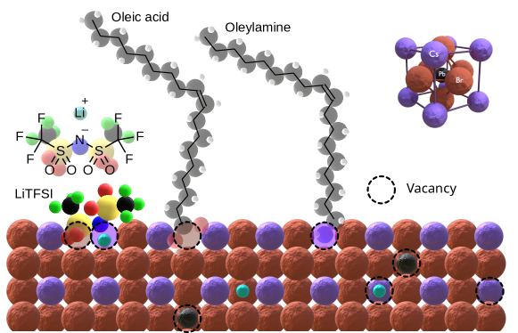
LHP NCs are typically synthesised as colloidal suspensions stabilised by organic ligands, such as oleic acid and oleylamine (see Fig. 1).11 Despite their high photoluminescence, these pristine “solutions” cannot be used directly for film fabrication and implementation in PeLEDs due to the electrically insulating nature of the ligands. Moreover, non-binding excess ligands, required to stabilise the suspensions, even deteriorate charge injection into the NCs further.12, 13, 14 “Washing” the nanocrystals before film deposition removes these ligands partially, however, at the expense of creating a large density of surface defects with the concomitant formation of non-radiative exciton decay channels mainly caused by A- and X-site vacancies, as well as inducing stability issues. To overcome these problems, a variety of different surface passivation strategies have been developed and employed in LHP NCs, including halide salts, strongly binding organic ligands and zwitterionic species.15 In particular, the use of lithium halides has been shown to increase the photoluminescence yield as well as their stability.16 Therein, its passivation is mostly attributed to the excess halides that fill the corresponding vacancies at the NC surface and, thus, reduce non-radiative defects and, at the same time, suppress ion migration via these vacancies. Nevertheless, the role of the Li+ cation itself has largely remained elusive.17 In this work, we show that by adding an organic lithium salt, viz. Lithium bis(trifluoromethanesulfonyl)imide (LiTFSI, see Fig. 1), to various LHP NC solutions, with emission colours ranging from deep red, via green to sky blue, their optoelectronic properties are tuned towards higher photoluminescence quantum yield, better hole injection and transport, as well as lower electroluminescence turn-on voltage. Overall, this results in a four- to seven-fold increase of the external quantum efficiency of PeLEDs.
2 Results and Discussion
2.1 Surface ligand exchange
LHP NCs with different stoichiometry and emission colour, ranging from sky blue (CsPbBr2Cl), via green (CsPbBr3) to red (MAPbBrI2, where MA stands for methylammonium), have been obtained commercially or synthesised as described in the Methods section. The native NC solutions with oleylamine and oleic acid surface ligands (10 mg/ml solid NC contents in toluene) have subsequently been mixed with equal volumes of LiTFSI solutions in chlorobenzene; see Methods for details. This has resulted in different weight concentrations of LiTFSI relative to the LHP NCs, such as 0.1 wt. %, 1 wt. %, 9 wt. % and 50 wt. %. Thin films have been prepared by spin-coating under inert atmosphere using these LiTFSI:NC mixed solutions, and their properties compared with corresponding thin films made from the native NC solutions. In the following, we focus on green CsPbBr3 NCs; blue and red NCs are only discussed in the LED part of this manuscript, but we anticipate that they behave qualitatively similar regarding the effect of LiTFSI on optical, electronic and charge transport behaviour.
In general, film formation without and with LiTFSI is found to be very similar (see Fig. S4) so that we will not discuss this in detail here. CsPbBr3 NCs of size 7-8 nm arrange in a cubic packing of the NCs on the surface of various kinds of substrates. We do not find a significant difference in NC arrangement and coverage, indicating that the addition of LiTFSI to the NC solutions preserves a certain fraction of the native oleylamine and oleic acid ligands, as schematically shown in Fig. 1. These films were subsequently studied by photoluminescence, photoelectron spectroscopy, density functional theory modelling, and in PeLEDs.
2.2 Photoluminescence
Photoluminescence quantum yield (PLQY) and lifetime are key indicators for the structural intactness of the LHP NC surfaces, both in solution as well as in thin films. Thereby, not only ligand passivation plays a key role but also their dielectric environment and the substrate on which they are deposited. Fig. 2 a shows a comparison of PLQY of native, i.e. oleylamine/oleic acid-capped, CsPbBr3 NCs on various substrates relative to glass (bk7). When using highly conductive substrates like metals, ITO, ZnO or PEDOT:PSS the PLQY is significantly lowered compared with glass. For PEDOT:PSS the quantum yield reduction can be ascribed to residual water content which may degrade the LHP NC significantly and quench luminescence.18, 19 The reduction for ZnO and ITO however originates from a different mechanism; e.g. their high carrier densities may enable exciton-carrier quenching or the oxides could lead to degradation of the LHPs.20 And even in the case of the organic polymer Polyvinylcarbazole (PVK), used as hole transporting layer (HTL) in PeLEDs, the PLQY is slightly lowered with respect to glass. However, by introducing LiTFSI as dopant in PVK the impairment is overcome. LiTFSI as dopant in HTLs is reported to increase their electrical conductivity rendering this effect rather unexpected.21 Another Li-based substrate treatment is a thin film of LiF evaporated on glass before spin-coating of the LHP NCs, which proves to be even more beneficial on the PLQY (see Fig. 2 a). A positive effect of an LiF interlayer has already been observed for light emission from bulk perovskites. Bigger grain sizes and reduced pinholes in the film were identified as the main cause for a better optical performance.22 For LHP NCs the grain sizes are predefined during synthesis and not expected to change upon spin-coating on a substrate.11 Consequently, it is reasonable to suspect a different mechanism for the PLQY enhancement.
This raises the question, whether the nature of the substrate alone affects the PLQY, or if there is interdiffusion from the underlying material into the LHP NC thin film. Thus, to study the influence of LiTFSI on the CsPbBr3 NCs, we directly add the Li salt to the solution prior to spin-coating on glass. Even though a more polar solvent, viz. chlorobenzene, is needed to mix the two substances, an increase in PLQY can be observed, both, in solution and as a thin film. Fig. 2 b shows the PLQYs of thin-films fabricated with different LiTFSI mass percentage mixing ratios. At very low concentrations, the PLQY is slightly decreased with respect to the pristine (0 wt. %) LHP NC film, which has a PLQY of about 70 %. In contrast to that, at concentrations higher than 1 wt. %, the PLQY is significantly increased reaching near unity at 9 wt. %, before it decreases again for a 1:1 mixture of both components. The PLQY impairment at low concentrations is comparable to a solvent mixture of toluene and chlorobenzene (but no LiTFSI), which may imply that some of the NCs are irreversibly degraded by the polar solvent before this detrimental effect is outweighted at higher LiTFSI content.23
Since we suspect a surface trap passivation effect by the LiTFSI, time-resolved photoluminescence (TRPL) has been measured on the same films (Fig. 2 c). As detailed in the Supporting Information (Fig. S1 & 2), the PL transients show a double-exponential decay with a fast initial lifetime of about 1 ns and a slower one with several nanoseconds. Weighting the lifetimes with their relative amplitudes, one obtains an average lifetime, as explained in the context of Fig. S1 & 2. For the native sample avg = 1.7 ns is obtained, whereas all the LiTFSI doped ones have similar avg = 2.6 ns, with only minor variation avg = 0.1 ns (see Fig 2 c), which is surprising in view of the observed changes in the PLQY over the same concentration range. However, as already discussed, the PLQY is reduced if there are solvent-degraded LHP NCs in the film, caused by their optically passive absorption. On the other hand, the PL lifetimes do not necessarily have to be affected by the degraded LHP NC if they do not emit any light and also do not interact with the optically active ones.
As the double-exponential fits on the intensity decay (see Fig. S1 & 2) reveal, the individual PL lifetimes are concentration independent (just like the average, avg). However, a comparison of the amplitudes exhibits a shift of weights towards the longer lifetime with increasing LiTFSI concentration. Together with the PLQY measurements, this implies that within the short lifetime there are more non-radiative decay processes. Furthermore, this could indicate that trap-assisted recombination is suppressed by the presence of LiTFSI. There have been several reports about surface trap passivation featuring various halide salts. They agree on a passivation mechanism by halide abundance, which has also been reported by groups using lithium-free halide salts.24, 25, 26, 27 However, in our case the halide-free LiTFSI seems to have a similar effect.
In addition to the changes in PLQY and PL lifetime, we observe a change of the radiation pattern of LHP NC films upon addition of LiTFSI. Fig. 2 d shows the parallelly polarised (p-pol.) angular dependent photoluminescence (ADPL) of a native and a 1 wt. % LiTFSI-treated CsPbBr3-NC thin film. As studied in great detail for organic light emitters28 as well as for some LHP NCs,29, 30 such radiation patterns contain information about the average orientation of the transition dipole moments (TDM) of the electronically active optical transition from the excited state to the ground state. This parameter is key to understanding and improving light outcoupling from thin-film light-emitting structures, such as organic LEDs28 or PeLEDs.31 In particular, the orientation parameter (which is defined as the fraction of power emitted by vertical TDMs) directly indicates the degree of anisotropy of the TDM orientation distribution, with being the isotropic case, and larger (smaller) values indicating more vertical (horizontal) TDM orientation. By comparing native CsPbBr3 and LiTFSI-treated NCs we notice a significant change of the TDM orientation. After fitting with an appropriate dipole model (details in the SI) a TDM orientation parameter of native = 0.51 is obtained, proving more vertical TDM orientation for the native NCs, in contrast to LiTFSI = 0.32 being close to isotropic for the 1 wt. % LiTFSI-treated NCs. This means that the unfavourable vertical TDM orientation of the native NC film is changed to an isotropic emission profile corresponding to the cubic structure of LHP. A similar behaviour has also been found by an Al2O3 overcoating of LHP nanoplatelets.32, 29 Thus, we suppose that LiTFSI acts as a dielectric layer to screen the asymmetry in the electrostatics between the substrate and the free surface of the NCs.
2.3 Energy Level Alignment
In order to elucidate the impact of LiTFSI on the electronic properties of LHP NCs, ultraviolet and X-ray photoelectron spectroscopy (UPS and XPS) measurements have been conducted on the PVK/CsPbBr3-NC and PVK/CsPbBr3-NC:LiTFSI films, respectively. As shown in Fig. 3 a by the valence region and the secondary electron cut-off spectra, the PVK film exhibits an initial work function of 4.59 eV and the highest occupied molecular orbital (HOMO) level is found at 1.37 eV binding energy (with respect to EF). Upon deposition of CsPbBr3-NCs, the work function decreases to 4.25 eV, likely due to the formation of band bending and/or an interface dipole at the buried interface.34 The valence band (VB) onset of CsPbBr3 is then extrapolated at 1.68 eV with respect to EF. Given the energy gap of CsPbBr3 of about 2.4 eV (515 nm), this shows that EF is located above mid-gap which is due to a strong n-type character on the surface of the NCs. Additional surface photovoltage measurements under white light illumination shows no shifts of CsPbBr3-NC energy levels, indicating a flat band condition through the LHP NC layer.35 Hence, the surface energy levels is then expected to also reflect the electronic properties within LHP NC thin-film. With the addition of LiTFSI to the CsPbBr3-NCs, a shift of the CsPbBr3-NC valence band towards lower binding energy by 0.25 eV is observed, which is accompanied by an increase of sample work function, leading to a decrease of VB onset to 1.43 eV with respect to EF. A similar shift of the core levels has been observed in XPS (see Fig. S5). Such a rigid shift of all CsPbBr3-NC energy levels distinctly demonstrates a p-doping effect by the addition of LiTFSI. It is worth mentioning that the use of substantially attenuated UV flux (attenuation of more than 100 times compared to the standard helium discharge lamp) is required for the UPS measurement, as a high UV flux is found to cause irreversible changes of the electronic structure. However, this leads to insufficient signal-to-noise ratio at the top VB region, which refrains us from extracting the LHP NC valence band onset on a logarithmic intensity scale of the photoelectron signal, as is known to accurately infer the band edge position of perovskite films due to the low density of states at the top of the valence band.36, 37 However, the shift of the electronic levels is not affected by this procedure. The energy level diagram of the PVK/CsPbBr3-NC stack is shown in Fig. 3 b. It can be clearly seen that PVK/CsPbBr3-NC interface initially exhibits a large energy barrier of ca. 0.31 eV for hole injection. Due to the p-doping effect by addition of LiTFSI, such energy barrier is reduced to 0.06 eV with CsPbBr3-NC VB edge shifting closer to the HOMO level of PVK. With such reduction, the hole injection can be significantly improved.
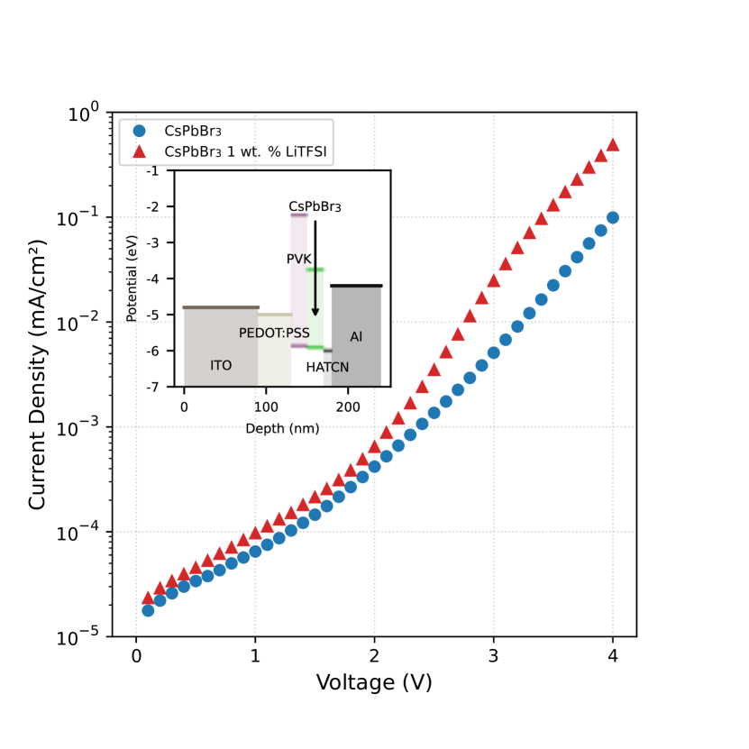
The reduced hole injection barrier is manifested in the electrical transport behaviour as well. As expected a single carrier hole-only device (layer stack shown in the inset of Fig. 4) with 1% LiTFSI doping shows a significant increase, respectively doubles the current density when operated at 4 V (see Fig. 4). We note that this current enhancement is not caused by a change of the layer morphology (including its thickness). As shown in the Supporting Information (Fig. S4), both native and LiTFSI-treated CsPbBr3-NC films have similar morphology with a partially closed uppermost NC monolayer on top of fully closed layer(s) underneath. It rather seems that the LiTFSI treatment improves the film morphology so that the increase of current cannot originate from insufficient NC coverage. Further, one can also expect to obtain different electronic coupling among the CsPbBr3-NCs by replacing (part of) the insulating oleylamine/oleic acid ligands by LiTFSI so that an improved bulk charge transport might also contribute to the observed current enhancement.
2.4 Density Functional Theory Modelling
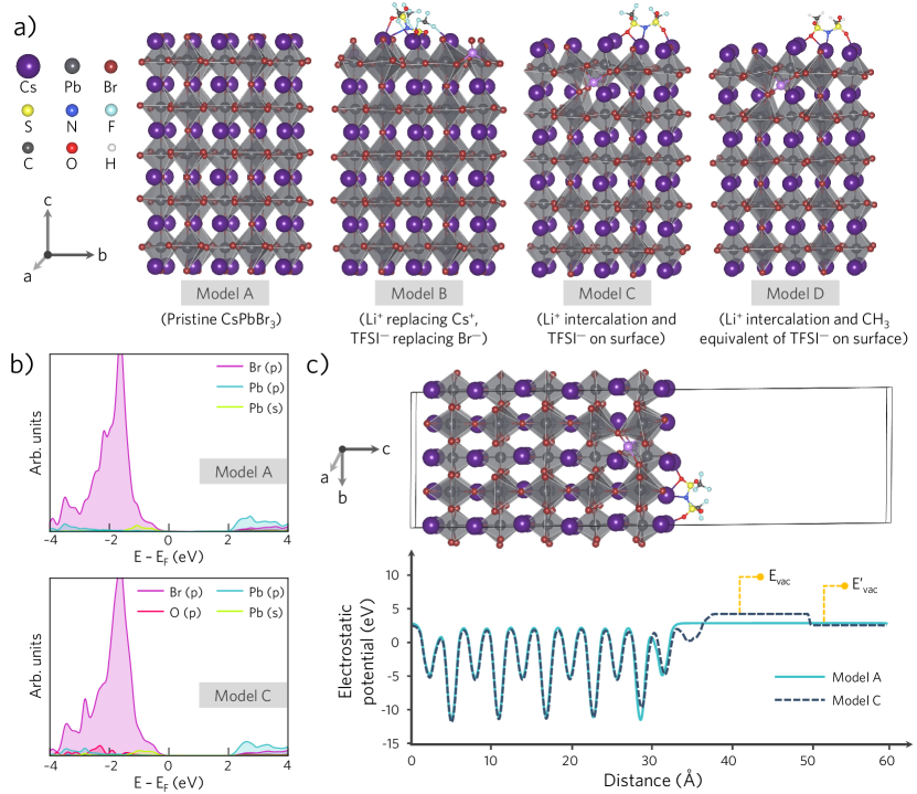
Density functional theory (DFT) modelling of four slab models was performed (see Supporting Information for computational details) to understand the structural changes upon LiTFSI treatment and its consequent impact on the electronic structure of the CsPbBr3 NCs. As shown in Fig. 5 a, model A consists of pristine CsPbBr3, while in model B, a Li+ ion replaces a Cs+ ion together with a TFSI− replacing a Br− ion over the surface. Model C considers intercalation of a Li+ ion, with one TFSI− placed over the CsBr-terminated surface, while model D is a system analogous to model C, but with the two –CF3 groups of the TFSI− ion having been replaced with two –CH3 groups.
Even though model D is not relevant experimentally, we explored this system computationally to disentangle the effect of C–F bond polarity on work function (WF), by closely comparing it with its C–H analogue.
We found that both pristine and LiTFSI-doped systems exhibit a very similar density of states (Fig. 5 b), and the orbital contributions from the TFSI− ions are quite deep-lying, appearing only near -2.0 eV. On the other hand, the TFSI− ligands were found to alter the surface dipole moment of the particle significantly, causing a substantial shift in the vacuum level (Fig. 5 c). Consequently, the mere presence of a surface TFSI− ion in model B replacing a Br− ion increased the work function of the NC from 4.51 eV in pristine model A to 5.54 eV in model B. The vacuum level-shift is even more prominent in model C, partly attributable to the fact that the dipoles caused by the surface TFSI− ions are now exclusively outside the inorganic core, as opposed to model B, where the O-atom from TFSI binds to a Pb2+ ion from the core and hence, the dipole is partly compensated. In model D, we show that when the highly polar C–F bonds in TFSI are replaced with C–H bonds, the vacuum level shift is drastically reduced (Evac = 4.23 eV and WF = 6.20 eV for –CF3 groups in model C vs. Evac = 3.83 eV and WF = 5.69 eV for –CH3 groups in model D). We recognize that the computed change in the work function is rather substantial compared to the experiment (UPS measured hole stabilisation being around 0.25 eV, Fig. 3 b). We attribute this discrepancy to (i) a higher TFSI− coverage in the model system compared to the experiment and (ii) the fact that in the slab model only one surface is asymmetrically covered with organic ligand as opposed to all six-side coverage in an actual NC.
Besides the change in work function, the topotactic intercalation of the Li+ ion, irrespective of whether in a tetrahedral or an octahedral site, has been demonstrated to increase interaction with neighbouring halide ions (see Li–Br bonding in addition to the usual Cs–Br bonds in model C and D in Fig. 5 a),17 and thus the activation barrier for halide ion migration is expected to increase.38 We anticipate a similar effect of the Li+ ion on preventing ion migration and improving the structural integrity of the LiTFSI-treated CsPbBr3 particles. Finally, we speculate that the availability of electronegative O-atoms from the TFSI− ligand, which is quite mobile over the surface, would also coordinate to Pb-atoms, as seen in model B, and contribute towards preventing detrimental Pb2+ to Pb0 reduction over the surface.39
2.5 Perovskite Light-emitting Diodes
Finally, we have employed native and LiTFSI-treated CsPbBr3 NCs in PeLEDs, where PVK is used as polymeric hole transport layer and B3PYMPM as electron transport layer, followed by a LiF/Al cathode as depicted in the inset of Fig. 6 a, the corresponding current-voltage-luminance characteristics is also shown in Fig. 6 a. The native CsPbBr3-NCs show two onsets for the current, with the first occurring slightly above 1 V which can be assigned to electrons due to the n-type position of the Fermi level; the second onset with a much steeper increase of current is located at about 3.5 V and would accordingly correspond to the onset of hole injection. This is supported by the fact that detectable luminance () occurs not before the applied voltage exceeds 4 V.
For the 1 wt. % LiTFSI-doped NCs, the double-step feature in the current disappears; rather, there is a steep increase starting above 2 V and luminance is detected already at 3 V. With further increasing voltage, both current and luminance increase much steeper in the LiTFSI-doped PeLED as compared to the untreated one. Finally, at 7 V both devices reach the same current, but the luminance in the LiTFSI-doped PeLED stays several times above the native one, indicating higher external quantum efficiency (EQE). This is shown in Fig. 6 c where the maximum EQE increases by more than a factor of 4 from 0.2 % to above 0.8 %. We also note that both, native and LiTFSI-treated CsPbBr3, PeLEDs have the same narrow green electroluminescence spectrum shown in the inset of Fig. 6 c.
As a proof of concept, we also applied LiTFSI doping to sky-blue emitting CsPbBr2Cl-NCs (results shown in Fig. 6 b,d). In this case, the reduction of the turn-on voltages for current and luminance induced by LiTFSI doping is even bigger, as detectable luminance sets in already below 3 V. The EQE is enhanced by a factor 7 from 0.1 % to 0.7 %, proving an even stronger effect of LiTFSI doping in the wider band-gap, sky-blue PeLEDs.
Furthermore, a red methylammonium-PbBrI2-NC PeLED can also be improved by LiTFSI, without an evident current-density increase (see Fig. S7). In this case, the red NC emitter does not face the same hole injection barriers as its blue and green counterparts, such that an increase in hole-injection is not expected to play a major role. Nevertheless, the device EQE is boosted by a similar factor through the LiTFSI treatment.
2.6 Discussion
The overall increase in PeLED performance with various LHP species implies a very versatile mechanism. The increase in PLQY and exciton lifetime with the LiTFSI concentration suggests a surface passivation mechanism. This has already been reported with lithium halides, where the lithium ions as well as the halides have shown surface trap passivation.16, 17, 40 However, the influence of Li+ has not been completely disentangled from the halide ones. Here the anion is not a halide, but the organic TFSI− ion, proving that a halide-free enhancement is possible. Still, the TFSI may not be a passive agent on the surface of LHP NCs. As sulfonic moeities have been reported to fill halide vacancies, a similar interaction from TFSI may be thinkable.10 Ultimately, a similar passivation as reported from lithium halides can be assumed.
Though, upon considering the PLQY and EQE depending on LiTFSI concentration (Fig. 2 b) it becomes evident, that another mechanism is present. The different dependence on LiTFSI concentration between EQE and PLQY cannot fully be explained by a surface trap passivation mechanism, since the EQE () is proportional to the PLQY:
| (1) |
However, at small doping concentrations the drop in EQE is not as pronounced as it is for the PLQY. Other factors only influencing the EQE are the outcoupling factor () and the charge carrier balance ().28 So an emitter orientation change can enhance the EQE compared to the PLQY, by a limited amount. This change in radiation pattern is observed as shown in Fig. 2 d, but the change of orientation is simulated to result in an EQE increase factor of only 1.3. Considering the PeLED fabricated with a 1 wt. % LiTFSI doping, as compared to the one with native CsPbBr3-NCs, the PLQY does not change significantly but the EQE does from about 0.2 % to 0.8 % by a factor of 4. The orientation alone cannot account for such large enhancement, but the last factor, the charge carrier balance can. Consequently, the doping procedure modifies the charge carrier balance in favour of EQE. Further investigations into that have been made by designing a hole-only device. This device exhibits hole-currents up to a factor 6 higher for the doped sample (see Fig. 4), implying an increased hole injection of roughly the same factor. The leveraged hole-injection can be ascribed to an improved VB alignment with the adjacent PVK’s HOMO level, as measured by UPS and XPS (see Fig 3). The injection barrier is reduced from 0.31 eV to 0.06 eV, which is in accordance with the increased hole current in the devices. At that, not only the VB onset is shifted but the entire density of states by 0.25 eV, raising the CB level by the same amount and rendering the CsPbBr3-NC semiconducting thin-film less n-type. Thus, excess electron injection is reduced as well. The significance of the VB alignment can be seen when comparing the differently coloured LEDs: For the blue CsPbBr2Cl the enhancement of current and EQE is highest, it decreases in green CsPbBr3 to no significant current increase for the red MAPbBrI2. The sky-blue CsPbBr2Cl has a VB onset reported to be even lower,41 rendering a potential p-doping even more beneficial as observed. The red device presumably does not benefit by the energy level shift, since because of its small bandgap41 the injection barrier has not been the limiting factor, even though the EQE is still increased significantly.
When considering the higher doping concentrations, 5 wt. % and more, a drop in luminance at elevated currents can be observed (see Fig. S6). Though the currents are further increasing the luminance does not exceed 20 cd/m2. A drastic EQE drop occurs at this critical luminance value. This drop is proven to be irreversible by multiple measurement runs of the LEDs. Apparently, there is a degradation induced by an excess of LiTFSI doping. Different interactions of lithium ions with the LHP NCs ranging from residing on an interstitial position over cation exchange (Cs+ for CsPbBr3) to filling lead vacancies have been explored.17 Upon excess doping multiple of these interactions may mix and change the LHP NCs properties towards less stability and quantum yield. Even though this drop in quantum yield is observed in PLQY measurements at 50 wt. % doping only, the drop in operational stability is already dominant for the PeLEDs starting from 5 wt. %. The degradation above a certain luminance together with the fact that CsPbBr3 is optically stable even upon strong excitations,42, 43 leads to the conclusion, that the degradation has to originate from an interaction between charge carriers and the excited state. Due to the revealed n-type nature of the LHP NCs and the different current onsets observed in the j-V-L curves, it is evident that there is an electron abundance in the device during light-emission. Several reports suggest a chemical reduction reaction of lead as a major degradation path in LHPs,44, 45 which may be facilitated by this surplus of electron in PeLEDs during operation. Finally the trion state, consisting of two electrons and one hole, may be the main cause of degradation. LiTFSI seems to have no influence on this proposed electron-induced degradation, since it only plays a minor role in the mitigation of electrons if at all. Its major contribution is ascribed to the easier hole injection into the LHP NCs not necessarily caused by the slightly less n-type energy alignment but rather by the reduced hole injection barrier. As a consequence the degradation seems to affect the EQE in PeLEDs significantly. With the red and blue device the LiTFSI has proven to be very versatile not only increasing the performance of simple all-inorganic tri-bromide LHP NCs, but also in mixed halide or organic perovskite NCs. However the degradation of PeLEDs cannot be prevented by the use of LiTFSI, since its major influence is related to hole-injection and increased PL quantum efficiency.
3 Conclusion
Surface passivation chemistry has already been recognised as key to enhance the performance of LHP NCs regarding its optoelectronic properties. Here we investigate surface treatment with a p-dopant, viz. the organic lithium salt LiTFSI, and show that the efficiency in PeLEDs is tremendously enhanced. We trace this enhancement back to positive effects on three decisive properties considering their EQE: the emitter’s quantum yield is proven to be brought close to unity. This is achieved by most surface passivation techniques on LHP NCs. Additionally, the angular emission pattern is changed in favour of better light outcoupling. While these two effects contribute to the increased efficiency to a certain extent, the most pronounced influence is identified to be the simultaneous tuning of the charge carrier balance to promote hole injection. Enhancement in these three key factors is a remarkable feature that can be attributed to the LiTFSI treatment. However there are still challenges concerning stability, which is still a major issue for LHP NCs in LEDs in general. At the same time the interaction as well as degradation of LHP NCs in conjuction with LiTFSI is not entirely understood. Nevertheless, a 4-7 fold increase in EQE can be achieved for PeLEDs of various colours and chemistry, rendering the LiTFSI treatment a very promising procedure to further investigate on.
4 Methods
4.1 Materials
The ITO (Indium Tin Oxide) substrates with dimensions 2 by 2 cm have been purchased by Kintec (Hongkong) with and without custom pattern of layer thickness 100 nm on a 23 nm SiO2 buffer on a 0.7 mm thick glass substrate. Fused Silica (SiO2) substrates with dimensions 2 by 2 cm have been bought with a thickness of 0.7 mm from Nano Quarz Wafer Germany GmbH. PEDOT:PSS is used in a low-conductive ratio of 1:20, having the descriptor CH8000, by Heraeus Germany GmbH & Co. KG. ZnO has been systhesised from Zincacetate with the sol-gel method.46 CsPbBr3 solution (c = 10mg/ml in toluene, ProductID: 900746) and LiTFSI (Lithium bis(trifluormethane)sulfonimide, 99.95 % trace metal basis, ProductID: 544094) have been ordered from Merck Germany KGaA. PVK (Poly(9-vinylcarbazole), Mw>105, ProductID: LT-N4078) has been obtained from Luminescence Technology Corp. (Lumtec, Taiwan).
4.2 Nanoparticle Preparation
Preparation of oleylammonium halide (OLA-HX)
To prepare a 1.1 mmol/ml OLA-HX precursor solution, 10 ml of oleylamine (OAm) has been placed in a 25-ml three-neck flask and either 1 ml of concentrated hydrochloric acid (HCl(aq.)) or 1.28 ml of concentrated hydrobromic acid (HBr(aq.)) has been added slowly. Subsequently, the solidified reaction mixture has been heated at 120 °C under nitrogen atmosphere for 2 hours. The reaction temperature has then been increased to 150 °C for 30 minutes and afterwards allowed to cool to room temperature. The mixture has been kept in a glovebox and heated to 80 °C before injection.
CsPbBr2Cl nanocrystals
CsPbBr2Cl Nanocrystals have been made by a Hot-Injection synthesis using a modified literature method.24 To synthesise 7 nm CsPbBr2Cl nanocrystals, 49 mg (0.15 mmol) Cs2CO3, 67 mg (0.3 mmol) PbO and 1.5 ml oleic acid (OA) have been degassed in 15 ml ODE in a 50 ml three-neck flask under reduced pressure at 120 °C for 1 hour. The temperature has been increased to 240 °C under nitrogen atmosphere, 1 ml OLA-HBr and 0.5 ml OLA-HCl precursor have been quickly injected and after one minute the reaction mixture has been cooled to room temperature using an ice-bath (below 180 °C). CsPbBr2Cl NCs have been collected by centrifuging the suspension (7000 rpm, 10 min.), decanting the supernatant, and collecting the precipitate. The precipitate has been centrifuged again without addition of a solvent (7000 rpm, 5 min.), and the resulting supernatant has been removed with a syringe, to separate the traces of residual supernatant. The precipitate has been dissolved in 2 ml hexane and centrifuged again (2500 rpm, 5 min.) to remove aggregates and larger particles. The resulting supernatant has been filtered through a 0.2 µm PTFE syringe filter and stored as stock solution inside of a glovebox with a typical concentration of 25 mM following Maes et al..47
LiTFSI treatement
The LiTFSI solutions are diluted from a stock which is created by dissolving 200 mg LiTFSI with 2 ml dimethylformamide (DMF) and 18 ml chlorobenzene (CB) by stirring overnight resulting in a volume concentration of 10 mg/ml. Dilution to 1, 0.1 and 0.01ṁg/ml concentration is done with CB only.
Equal volumes of LHP NC solution and LiTFSI solutions are mixed to obtain a LiTFSI-doped solution. Mixing equal volumes of 10 mg/ml LHP NC and 10 mg/ml LiTFSI yields a 5 mg/ml LHP NC solution with 50 wt. % LiTFSI doping. Analogously, a 9.09, 0.990 and 0.099 wt. % doped solution is obtained by using 1, 0.1 and 0.01 mg/ml concentrated LiTFSI solution and mixing with the 10mg/ml LHP NC solution by equal volumes. All LHP NC solutions are created within a nitrogen filled glovebox and have exhibited stable luminescence for at least 3 months at room temperature.
4.3 Sample Preparation
Photoluminescence
Fused Silica is used as a substrate for all PL measurements, that is PLQY, TRPL and ADPL. The substrates are spin-coated on in a nitrogen-filled glovebox by dropping 50 µl (p.r.n. LiTFSI-doped) LHP NC solution before starting the rotation of the spin-coater. After a settling time of 30 seconds it is accelerated to 500 rpm and kept at that speed for another 30 seconds. To remove residuals from the edges, spinning for 5 seconds at 2000 rpm is applied before stopping the procedure.
UPS/XPS, SEM, LEDs and hole-only devices
For UPS/XPS and SEM the unpatterned, and for the electrical devices the patterned ITO substrates are used. Initally, PEDOT:PSS is spin-coated in the cleanroom, at 4000 rpm for 30s, and heated on a hotplate at 130 °C for 15 minutes, resulting in a smooth approx. 40 nm thin film. The samples are transferred to a nitrogen-filled glovebox immediately. As second layer, the approx. 20 nm thin PVK film is deposited by spin-coating a 3 mg/ml concentrated PVK-chlorobenzene solution at 3000 rpm for 30 seconds and heating at 175 °C for 30 minutes. The LHP NC solutions are spin-coated as described for the PL samples, after cooling the substrate to room-temperature, resulting in a closed film of about 2-3 monolayers (effective thickness approx. 20 nm).
The sample in current state, that is the bottom-half LED, is used for UPS/XPS and SEM investigations. For devices, the samples are transferred without ambient exposure into a high vacuum chamber, with a pressure smaller than 10-6 mbar. For hole-only, 10 nm HATCN (rate: 50 pm/s), for LEDs 55 nm B3PYMPM (rate: 100 pm/s) followed by 0.5 nm LiF (rate: 10 pm/s) is evaporated. The devices are finished with a 60 nm (rate: 100 pm/s) thick Aluminium cathode, also deposited by thermal deposition.
4.4 Measurement details
PLQY
The PLQY is determined by a two-step-method measurement featuring a BaSO4 coated integrating sphere.48 The excitation source is a HeCd laser’s 442 nm light. The excitation signal as well as the samples fluorescence is collected with a fiber and guided into a Princeton Instruments Acton2300i spectrometer, which is connected to a nitrogen cooled CCD camera, that is Princeton Instrument’s Pylon BRX100. An absolute calibration of the integrating-sphere-CCD system has been performed with a lamp calibrated for spectral irradiance according to the NIST standard by GigaHertz Optik GmbH Germany. With that system spectra could evaluated to its amount of photons and consequently a PLQY is calculated.
ADPL
The ADPL measurement and analysis were performed as previously reported by our group.31 The spectrum is recorded with the same CCD-Spectrometer system as explained for the PLQY.
TRPL
Transient Photoluminescence was recorded by the C5680 streak camera system by Hamamatsu, after being delayed by DG535 by Stanford Instruments while being spectrally analysed by a Acton Spectra Pro 2300i. Excitation was done with the EKSPLA PT400 Diode Pumped Solid State laser set to wavelength 355 nm.
UPS/XPS
Ultraviolet photoelectron spectroscopy (UPS) measurements have been conducted using a SPECS PHOIBOS 100 hemispherical electron analyser equipped with a monochromatised helium discharge lamp (21.22 eV). The UV flux has been attenuated significantly by the monochromator to avoid UV-induced sample degradation. A sample bias of -10 V has been applied to acquire the secondary electron cutoff spectra. The base pressure of the analysis chamber has been kept below 10-9 mbar. X-ray photoelectron spectroscopy (XPS) measurements have been performed at a JEOL JPS-9030 ultrahigh vacuum system (base pressure of 10-9 mbar) using monochromatised Al K (1486.6 eV) radiation. Anode power of 30 W was applied for XPS measurements, which has not been found to induce noticeable sample degradation.
LEDs and hole-only devices
j-V(-L) curves are recorded with a Keithley 2612B Source Meter Unit (SMU). A Photodiode of known diameter at known distance is used for Luminance detection. The electroluminescent spectrum is taken with the Phelos system by fluxim AG (Switzerland). With that and a lambertian approximation the EQE is determined. The integrity of the lambertian approximation has been ensured by random sampling with a calibrated integrating sphere (same setup as for PLQY). The sampling revealed that the photodiode’s and consequently in this manuscript reported EQE is about 10 % underestimated, relatively. For instance the EQE of the 9 wt. % LiTFSI-doped sample in Fig. 2 b has shown 1.1 % EQE in the integrating sphere while it has been 1 % in the photodiode-setup.{acknowledgement}This work was funded by Deutsche Forschungsgemeinschaft (DFG) within Priority Program SPP2196 ("Perovskite Semiconductors: From Fundamental Properties to Devices") under project nos. 424708673 and 423749265, as well as by their Heisenberg Program under grant SCHE1905/9-1. M.M. acknowledges postdoctoral support from the Alexander von Humboldt Foundation.{suppinfo}The following supporting material is available:
-
1.
TRPL-fits and details (Fig. S1 & S2).
-
2.
ADPL-fits and details (Fig. S3).
-
3.
SEM images (Fig. S4).
-
4.
XPS spectra (Fig. S5).
-
5.
Details on DFT calculations with respective structures for the slab models.
-
6.
CsPbBr3 NC LEDs at all LiTFSI concentrations (Fig. S6) and MAPbBrI2 NC LED details (Fig. S7).
-
7.
Additional details on chemicals and preparation.
References
- Era et al. 1994 Era, M.; Morimoto, S.; Tsutsui, T.; Saito, S. Organic-inorganic heterostructure electroluminescent device using a layered perovskite semiconductor (C6H5C2H4NH3)2PbI4. Applied Physics Letters 1994, 65, 676–678
- Coelle et al. 2001 Coelle, M.; Bruetting, W.; Schwoerer, M.; Yahiro, M.; Tsutsui, T. Electroluminescent devices using a layered organic-inorganic perovskite structure as emitter. SPIE Proceedings. 2001
- Tan et al. 2014 Tan, Z.-K.; Moghaddam, R. S.; Lai, M. L.; Docampo, P.; Higler, R.; Deschler, F.; Price, M.; Sadhanala, A.; Pazos, L. M.; Credgington, D.; Hanusch, F.; Bein, T.; Snaith, H. J.; Friend, R. H. Bright light-emitting diodes based on organometal halide perovskite. Nature Nanotechnology 2014, 9, 687–692
- Liu et al. 2019 Liu, Y. et al. Efficient blue light-emitting diodes based on quantum-confined bromide perovskite nanostructures. Nature Photonics 2019, 13, 760–764
- Liu et al. 2020 Liu, X.-K.; Xu, W.; Bai, S.; Jin, Y.; Wang, J.; Friend, R. H.; Gao, F. Metal halide perovskites for light-emitting diodes. Nature Materials 2020, 20, 10–21
- Park et al. 2019 Park, M.-H.; Kim, J. S.; Heo, J.-M.; Ahn, S.; Jeong, S.-H.; Lee, T.-W. Boosting Efficiency in Polycrystalline Metal Halide Perovskite Light-Emitting Diodes. ACS Energy Letters 2019, 4, 1134–1149
- Ji et al. 2021 Ji, K.; Anaya, M.; Abfalterer, A.; Stranks, S. D. Halide Perovskite Light-Emitting Diode Technologies. Advanced Optical Materials 2021, 9, 2002128
- Woo et al. 2021 Woo, S.-J.; Kim, J. S.; Lee, T.-W. Characterization of stability and challenges to improve lifetime in perovskite LEDs. Nature Photonics 2021, 15, 630–634
- Kim et al. 2021 Kim, Y.-H. et al. Comprehensive defect suppression in perovskite nanocrystals for high-efficiency light-emitting diodes. Nature Photonics 2021, 15, 148–155
- Ye et al. 2021 Ye, J.; Byranvand, M. M.; Martínez, C. O.; Hoye, R. L. Z.; Saliba, M.; Polavarapu, L. Defect Passivation in Lead-Halide Perovskite Nanocrystals and Thin Films: Toward Efficient LEDs and Solar Cells. Angewandte Chemie 2021, 133, 21804–21828
- Protesescu et al. 2015 Protesescu, L.; Yakunin, S.; Bodnarchuk, M. I.; Krieg, F.; Caputo, R.; Hendon, C. H.; Yang, R. X.; Walsh, A.; Kovalenko, M. V. Nanocrystals of Cesium Lead Halide Perovskites (CsPbX3, X = Cl, Br, and I): Novel Optoelectronic Materials Showing Bright Emission with Wide Color Gamut. Nano Letters 2015, 15, 3692–3696
- Gomez et al. 2017 Gomez, L.; de Weerd, C.; Hueso, J. L.; Gregorkiewicz, T. Color-stable water-dispersed cesium lead halide perovskite nanocrystals. Nanoscale 2017, 9, 631–636
- Kumawat et al. 2018 Kumawat, N. K.; Swarnkar, A.; Nag, A.; Kabra, D. Ligand Engineering to Improve the Luminance Efficiency of CsPbBr3 Nanocrystal Based Light-Emitting Diodes. The Journal of Physical Chemistry C 2018, 122, 13767–13773
- Yan et al. 2021 Yan, W.; Shen, J.; Zhu, Y.; Gong, Y.; Zhu, J.; Wen, Z.; Li, C. CsPbBr3 quantum dots photodetectors boosting carrier transport via molecular engineering strategy. Nano Research 2021, 14, 4038–4045
- Li et al. 2018 Li, G.; Huang, J.; Zhu, H.; Li, Y.; Tang, J.-X.; Jiang, Y. Surface Ligand Engineering for Near-Unity Quantum Yield Inorganic Halide Perovskite QDs and High-Performance QLEDs. Chemistry of Materials 2018, 30, 6099–6107
- Wu et al. 2020 Wu, T.; Li, J.; Zou, Y.; Xu, H.; Wen, K.; Wan, S.; Bai, S.; Song, T.; McLeod, J. A.; Duhm, S.; Gao, F.; Sun, B. High-Performance Perovskite Light-Emitting Diode with Enhanced Operational Stability Using Lithium Halide Passivation. Angewandte Chemie International Edition 2020, 59, 4099–4105
- Wu et al. 2021 Wu, H.; Qiu, J.; Wang, J.; Wen, Y.; Wang, Q.; Long, Z.; Zhou, D.; Yang, Y.; Wang, D. The dual-defect passivation role of lithium bromide doping in reducing the nonradiative loss in CsPbX3 (X = Br and I) quantum dots. Inorganic Chemistry Frontiers 2021, 8, 658–668
- Nguyen et al. 2004 Nguyen, T.; Rendu, P. L.; Long, P.; Vos, S. D. Chemical and thermal treatment of PEDOT:PSS thin films for use in organic light emitting diodes. Surface and Coatings Technology 2004, 180-181, 646–649
- Peng et al. 2017 Peng, X.-F.; Wu, X.-Y.; Ji, X.-X.; Ren, J.; Wang, Q.; Li, G.-Q.; Yang, X.-H. Modified Conducting Polymer Hole Injection Layer for High-Efficiency Perovskite Light-Emitting Devices: Enhanced Hole Injection and Reduced Luminescence Quenching. The Journal of Physical Chemistry Letters 2017, 8, 4691–4697
- Olthof 2021 Olthof, S. Reactive interfaces: perovskite degradation at metal-oxide interfaces probed by photoelectron spectroscopy. Organic and Hybrid Light Emitting Materials and Devices XXV. 2021
- Kim et al. 2019 Kim, K.; Jeong, J.; Kim, M.; Kang, D.; Cho, S. W.; Lee, H.; Yi, Y. Direct p-doping of Li-TFSI for efficient hole injection: Role of polaronic level in molecular doping. Applied Surface Science 2019, 480, 565–571
- Zhao et al. 2020 Zhao, B.; Lian, Y.; Cui, L.; Divitini, G.; Kusch, G.; Ruggeri, E.; Auras, F.; Li, W.; Yang, D.; Zhu, B.; Oliver, R. A.; MacManus-Driscoll, J. L.; Stranks, S. D.; Di, D.; Friend, R. H. Efficient light-emitting diodes from mixed-dimensional perovskites on a fluoride interface. Nature Electronics 2020, 3, 704–710
- Sun et al. 2021 Sun, Y.; Zhang, H.; Zhu, K.; Ye, W.; She, L.; Gao, X.; Ji, W.; Zeng, Q. Research on the influence of polar solvents on CsPbBr3 perovskite QDs. RSC Advances 2021, 11, 27333–27337
- Dutta et al. 2019 Dutta, A.; Behera, R. K.; Pal, P.; Baitalik, S.; Pradhan, N. Near-Unity Photoluminescence Quantum Efficiency for All CsPbX3(X=Cl, Br, and I) Perovskite Nanocrystals: A Generic Synthesis Approach. Angewandte Chemie 2019, 131, 5608–5612
- Akkerman et al. 2015 Akkerman, Q. A.; D’Innocenzo, V.; Accornero, S.; Scarpellini, A.; Petrozza, A.; Prato, M.; Manna, L. Tuning the Optical Properties of Cesium Lead Halide Perovskite Nanocrystals by Anion Exchange Reactions. Journal of the American Chemical Society 2015, 137, 10276–10281
- Stasio et al. 2017 Stasio, F. D.; Christodoulou, S.; Huo, N.; Konstantatos, G. Near-Unity Photoluminescence Quantum Yield in CsPbBr3 Nanocrystal Solid-State Films via Postsynthesis Treatment with Lead Bromide. Chemistry of Materials 2017, 29, 7663–7667
- Woo et al. 2017 Woo, J. Y.; Kim, Y.; Bae, J.; Kim, T. G.; Kim, J. W.; Lee, D. C.; Jeong, S. Highly Stable Cesium Lead Halide Perovskite Nanocrystals through in Situ Lead Halide Inorganic Passivation. Chemistry of Materials 2017, 29, 7088–7092
- Schmidt et al. 2017 Schmidt, T. D.; Lampe, T.; M. R., D. S.; Djurovich, P. I.; Thompson, M. E.; Brütting, W. Emitter Orientation as a Key Parameter in Organic Light-Emitting Diodes. Physical Review Applied 2017, 8
- Jurow et al. 2019 Jurow, M. J.; Morgenstern, T.; Eisler, C.; Kang, J.; Penzo, E.; Do, M.; Engelmayer, M.; Osowiecki, W. T.; Bekenstein, Y.; Tassone, C.; Wang, L.-W.; Alivisatos, A. P.; Brütting, W.; Liu, Y. Manipulating the Transition Dipole Moment of CsPbBr3 Perovskite Nanocrystals for Superior Optical Properties. Nano Letters 2019, 19, 2489–2496
- Jagielski et al. 2020 Jagielski, J.; Solari, S. F.; Jordan, L.; Scullion, D.; Blülle, B.; Li, Y.-T.; Krumeich, F.; Chiu, Y.-C.; Ruhstaller, B.; Santos, E. J. G.; Shih, C.-J. Scalable photonic sources using two-dimensional lead halide perovskite superlattices. Nature Communications 2020, 11
- Morgenstern et al. 2020 Morgenstern, T.; Lampe, C.; Naujoks, T.; Jurow, M.; Liu, Y.; Urban, A. S.; Brütting, W. Elucidating the performance limits of perovskite nanocrystal light emitting diodes. Journal of Luminescence 2020, 220, 116939
- Jurow et al. 2017 Jurow, M. J.; Lampe, T.; Penzo, E.; Kang, J.; Koc, M. A.; Zechel, T.; Nett, Z.; Brady, M.; Wang, L.-W.; Alivisatos, A. P.; Cabrini, S.; Brütting, W.; Liu, Y. Tunable Anisotropic Photon Emission from Self-Organized CsPbBr3 Perovskite Nanocrystals. Nano Letters 2017, 17, 4534–4540
- Tavares et al. 2021 Tavares, T. B.; de Sousa, F. F.; Sales, M. J. A.; Paterno, L. G.; Paschoal, W.; Moreira, S. G. C. Optical and morphological features of poly(vinyl carbazole)/ferrite composites for potential opto-electronic applications. Applied Physics A 2021, 127
- Olthof and Meerholz 2017 Olthof, S.; Meerholz, K. Substrate-dependent electronic structure and film formation of MAPbI3 perovskites. Scientific Reports 2017, 7
- Zu et al. 2019 Zu, F.; Wolff, C. M.; Ralaiarisoa, M.; Amsalem, P.; Neher, D.; Koch, N. Unraveling the Electronic Properties of Lead Halide Perovskites with Surface Photovoltage in Photoemission Studies. ACS Applied Materials & Interfaces 2019, 11, 21578–21583
- Endres et al. 2016 Endres, J.; Egger, D. A.; Kulbak, M.; Kerner, R. A.; Zhao, L.; Silver, S. H.; Hodes, G.; Rand, B. P.; Cahen, D.; Kronik, L.; Kahn, A. Valence and Conduction Band Densities of States of Metal Halide Perovskites: A Combined Experimental–Theoretical Study. The Journal of Physical Chemistry Letters 2016, 7, 2722–2729
- Zu et al. 2019 Zu, F.; Amsalem, P.; Egger, D. A.; Wang, R.; Wolff, C. M.; Fang, H.; Loi, M. A.; Neher, D.; Kronik, L.; Duhm, S.; Koch, N. Constructing the Electronic Structure of CH3NH3PbI3 and CH3NH3PbBr3 Perovskite Thin Films from Single-Crystal Band Structure Measurements. The Journal of Physical Chemistry Letters 2019, 10, 601–609
- Cao et al. 2018 Cao, J.; Tao, S. X.; Bobbert, P. A.; Wong, C.-P.; Zhao, N. Interstitial Occupancy by Extrinsic Alkali Cations in Perovskites and Its Impact on Ion Migration. Advanced Materials 2018, 30, 1707350
- An et al. 2018 An, R.; Zhang, F.; Zou, X.; Tang, Y.; Liang, M.; Oshchapovskyy, I.; Liu, Y.; Honarfar, A.; Zhong, Y.; Li, C.; Geng, H.; Chen, J.; Canton, S. E.; Pullerits, T.; Zheng, K. Photostability and Photodegradation Processes in Colloidal CsPbI3 Perovskite Quantum Dots. ACS Applied Materials & Interfaces 2018, 10, 39222–39227
- Fang et al. 2018 Fang, Z.; He, H.; Gan, L.; Li, J.; Ye, Z. Understanding the Role of Lithium Doping in Reducing Nonradiative Loss in Lead Halide Perovskites. Advanced Science 2018, 5, 1800736
- Ravi et al. 2016 Ravi, V. K.; Markad, G. B.; Nag, A. Band Edge Energies and Excitonic Transition Probabilities of Colloidal CsPbX3 (X = Cl, Br, I) Perovskite Nanocrystals. ACS Energy Letters 2016, 1, 665–671
- Rainò et al. 2019 Rainò, G.; Landuyt, A.; Krieg, F.; Bernasconi, C.; Ochsenbein, S. T.; Dirin, D. N.; Bodnarchuk, M. I.; Kovalenko, M. V. Underestimated Effect of a Polymer Matrix on the Light Emission of Single CsPbBr3 Nanocrystals. Nano Letters 2019, 19, 3648–3653
- Pierini et al. 2020 Pierini, S.; D’Amato, M.; Goyal, M.; Glorieux, Q.; Giacobino, E.; Lhuillier, E.; Couteau, C.; Bramati, A. Highly Photostable Perovskite Nanocubes: Toward Integrated Single Photon Sources Based on Tapered Nanofibers. ACS Photonics 2020, 7, 2265–2272
- Samu et al. 2017 Samu, G. F.; Scheidt, R. A.; Kamat, P. V.; Janáky, C. Electrochemistry and Spectroelectrochemistry of Lead Halide Perovskite Films: Materials Science Aspects and Boundary Conditions. Chemistry of Materials 2017, 30, 561–569
- Mulder et al. 2021 Mulder, J. T.; du Fossé, I.; Jazi, M. A.; Manna, L.; Houtepen, A. J. Electrochemical p-Doping of CsPbBr3 Perovskite Nanocrystals. ACS Energy Letters 2021, 6, 2519–2525
- Hasnidawani et al. 2016 Hasnidawani, J.; Azlina, H.; Norita, H.; Bonnia, N.; Ratim, S.; Ali, E. Synthesis of ZnO Nanostructures Using Sol-Gel Method. Procedia Chemistry 2016, 19, 211–216
- Maes et al. 2018 Maes, J.; Balcaen, L.; Drijvers, E.; Zhao, Q.; Roo, J. D.; Vantomme, A.; Vanhaecke, F.; Geiregat, P.; Hens, Z. Light Absorption Coefficient of CsPbBr3 Perovskite Nanocrystals. The Journal of Physical Chemistry Letters 2018, 9, 3093–3097
- Leyre et al. 2014 Leyre, S.; Coutino-Gonzalez, E.; Joos, J. J.; Ryckaert, J.; Meuret, Y.; Poelman, D.; Smet, P. F.; Durinck, G.; Hofkens, J.; Deconinck, G.; Hanselaer, P. Absolute determination of photoluminescence quantum efficiency using an integrating sphere setup. Review of Scientific Instruments 2014, 85, 123115