On the Mitigation of Read Disturbances in Neuromorphic Inference Hardware
Abstract
Non-Volatile Memory (NVM) cells are used in neuromorphic hardware to store model parameters, which are programmed as resistance states. NVMs suffer from the read disturb issue, where the programmed resistance state drifts upon repeated access of a cell during inference. We show that resistance drifts can lower the inference accuracy. To address this, it is necessary to periodically reprogram model parameters to the hardware (a high overhead operation). We study read disturb failures of an NVM cell. Our analysis show both a strong dependency on model characteristics such as synaptic activation and criticality, and on the voltage used to read resistance states during inference. We propose a system software framework to incorporate such dependencies in programming model parameters on NVM cells of a neuromorphic hardware. At the core of our framework is a convex optimization formulation which aims to implement synaptic weights that have more activations and are critical, i.e., those that have high impact on accuracy on NVM cells that are exposed to lower voltages during inference. In this way, we increase the time interval between two consecutive reprogramming of model parameters. We evaluate our system software with many emerging inference models on a neuromorphic hardware simulator and show a significant reduction in the system overhead.
Index Terms:
Neuromorphic Computing, Read Disturbance, Non-Volatile Memory, Spiking Neural Networks.I Introduction
Neuromorphic systems are integrated circuits designed to mimic the neural architecture in primates. Here, neural circuity is tightly coupled with synaptic storage, which eliminates the performance and energy bottlenecks of shared-memory systems for machine learning inference [1]. Non-Volatile Memory (NVM) cells such as oxide-based resistive switching random access memory (OxRRAM) can implement multilevel analog operations, which make them ideal candidates for storing model parameters, i.e., the synaptic weights of a machine learning model [2].
For use as an inference hardware, trained model parameters are programmed as resistance states on OxRRAM cells of the hardware. Once programmed, the hardware is expected to perform inference continuously, without having to reprogram the model parameters. Unfortunately, OxRRAM cells suffer from the read disturb issue, where a cell’s resistance state may drift from its programmed value upon repeated access during inference [3]. We show that resistance drifts can lead to a lower inference accuracy (see Section VI).
One system-level technique to mitigate read disturbances in a neuromorphic hardware is to periodically reprogram the trained parameters to the OxRRAM cells of the hardware. Reprogramming of model parameters involves transferring the synaptic weights from the main memory (primary storage) to the neuromorphic hardware via bandwidth-limited memory channels (see Fig. 11). Additionally, NVM cells require the long-latency program-and-verify (P&V) scheme to configure their resistance states [4]. These factors increase the time it takes to reprogram model parameters on OxRRAM cells. When a model is being reprogrammed, the hardware is unavailable to perform inference operations. Therefore, the performance overhead associated with periodic reprogramming is
| (1) |
where defines the reprogramming time of the model and defines the interval at which the model is being reprogrammed to the hardware.
We show that periodic reprogramming leads to a high system overhead even for smaller models like LeNet and AlexNet, and is expected to become a critical performance bottleneck for emerging large models such as VGGNet, ResNet, and DenseNet. Our objective is to minimize this overhead by increasing the reprogram interval . To this end, we make the following three key observations.
Observation 1: Different synaptic connections of a machine learning model have different tolerance to resistance drift and they impact model accuracy differently. See Sec. II.
Observation 2: OxRRAM cells in a neuromorphic hardware exhibit variation in read disturbance due to a difference in the exposed read voltage used during inference. See Sec. III.
Observation 3: Activation of a synaptic connection in a model is workload-dependent and it leads to a difference in the amount of resistance drift within the model. See Sec. IV.
Based on these three observations, we propose a system software framework that incorporates this application and voltage-dependent characteristics of read disturbance of OxRRAM cells in implementing a machine learning model on the hardware. The key idea is to implement the synaptic weight of connections that have higher activations and lead to higher accuracy drop on NVM cells that are exposed to lower voltages during inference. In this way, we are able to sustain larger resistance drifts of synaptic weights before reprogramming of model parameters on OxRRAM cells becomes necessary.
A preliminary version of this system software framework is proposed in our prior work [5]. Here we extend this framework in four key directions – 1) introducing overhead due to reprogramming of model parameters as a key performance metric, 2) extending the system software framework to periodically reprogram model parameters to a neuromorphic hardware in order to maintain integrity of machine learning tasks, 3) a convex optimization formulation of cluster mapping to crossbar in order to reduce the system overhead, and 4) exploiting machine learning model characteristics to identify non-critical model parameters and eliminating them from the critical path of deciding the reprogramming interval. In this way, our convex optimizer is able to increase the reprogramming interval compared to [5], thereby significantly reducing the system overhead (see Section VI).
We integrate the proposed system software framework inside NeuroXplorer [6], a cycle-accurate simulator of neuromorphic hardware and evaluate it using five commonly-used machine learning inference applications. Results demonstrate an average 35% reduction of system overhead.
II Resistance Drift Tolerance of Machine Learnig Workloads
Synaptic connections of a machine learning workload have varying tolerances to resistance drift. This impacts accuracy differently. To illustrate this, we consider 2-bit quantized versions of five commonly-used convolutional neural networks (CNNs) – LeNet (1989), AlexNet (2012), VGGNet (2015), ResNet (2015), and DenseNet (2017). There are three weight levels used in these models, corresponding to ternary values of -1, 0, and +1 [7]. Figure 1 illustrates the fraction of total synapses in the fully-connected layer that leads to 1% or higher accuracy drop. We report results for the following four configurations – 1) resistance reduction by two levels (“-2”), 2) resistance reduction by one level (“-1”), 3) resistance increase by 1 level (“+1”), and 4) resistance increase by two levels (“+2”). 111We note that if a synaptic weight is +1, then the synapse is tolerant to resistance drifts in the positive direction. Similarly, if a synaptic weight is -1, then the synapse is tolerant to drifts in the negative direction. Such cases are included in the results of Figure 1. We make the following three key observations.
First, synapses in a machine learning model have varying tolerance to resistance drift. On average, only 35% of synapses show accuracy drop when their resistance drifts by two levels in the negative direction, only 66% when resistance drifts by one level in the negative direction, only 60% when resistance drifts by one level in the positive direction, and only 30% when resistance drifts by two levels in the positive direction. The reason for such variations is two-fold. First, most machine learning models are over-parameterized. Therefore, resistance levels of non-critical synapses do not impact the accuracy. Second, due to the approximate training using the backpropagation algorithm, a drift in the resistance level of some synapses may not impact accuracy significantly. To this end, we note that the synaptic weight value of a non-critical synapse may not necessarily be close to zero. It simply means that any change of its weight value may not impact accuracy. For this reason, any neuron and synapse pruning strategy such as [7] will not eliminate non-critical synapses that are non-zero.
Second, for LeNet, only a small fraction (less than 1%) of synapses lead to accuracy drop when resistance drifts by +1 and +2. This is because most of synaptic weights of LeNet are positive. So any transition in the positive direction results in no significant accuracy impact.
Third, tolerance to resistance drift depends on the specific CNN model and therefore, model-specific solutions are needed. Our proposed approach is the following. First, we identify the critical synapses, i.e., those that have high impact on accuracy by analyzing a CNN model. Next, we exploit device characteristics and mapping alternatives to minimize the negative impact of resistance drift.
To motivate our solution, we discuss resistance drift in NVMs, focusing on OxRRAM devices.
III Resistance Drifts in Non-Volatile
Memory Devices
III-A Oxide-based Resistive RAM (OxRRAM) Technology
The resistance switching random access memory (OxRRAM) technology presents an attractive option for implementing the synaptic cells of a crossbar due to its demonstrated potential for low-power multilevel operation and high integration density [2]. An OxRRAM cell is composed of an insulating film sandwiched between conducting electrodes forming a metal-insulator-metal (MIM) structure (see Figure 2). Recently, filament-based metal-oxide OxRRAM implemented with transition-metal-oxides such as HfO2, ZrO2, and TiO2 has received considerable attention due to their low-power and CMOS-compatible scaling.
Synaptic weights are represented as conductance of the insulating layer within each OxRRAM cell. To program an OxRRAM cell, elevated voltages are applied at the top and bottom electrodes, which re-arranges the atomic structure of the insulating layer. Figure 2 shows the High-Resistance State (HRS) and the Low-Resistance State (LRS) of an OxRRAM cell. An OxRRAM cell can also be programmed into intermediate low-resistance states, allowing its multilevel operations.
III-B Read Disturbance Issues of OxRRAM Cells
In OxRRAM technology, the transition from HRS to one of the LRS states is governed by a sudden decrease of the vertical filament gap on application of a stress voltage during spike propagation [3]. This is illustrated in the left subfigure of Figure 3 where the vertical filament gap is shown to reduce by an amount . This may result in a conducting filament between the two metal layers causing the resistive state to change from HRS to LRS. The rate of change of the filament gap of the OxRRAM cell is
| (2) |
In the above equation, defines the state transition time, is the initial filament gap of the OxRRAM cell, is the voltage applied to the cell, is the local field enhancement factor, which is related to the gap , is the atomic hoping distance, is the activation energy, is the Boltzmann constant, is the temperature (in Kelvin), is the length of the vertical filament, is the filament charge, is a constant related to vertical filament growth, and are fitting constants.
The transition from one of the LRS states is governed by the lateral filament growth [3]. This is illustrated in the right subfigure of Figure 3. The time for state transition in the OxRRAM cell is given by
| (3) |
If the state transition time of an OxRRAM cell is 1000 ms, then a single quasi-static read operating using one 1000 ms read pulse or equivalently, 1000 read accesses using 1-ms spike pulses can lead to an abrupt change in the cell’s state. 222Apart from resistance drift, there are also other forms of reliability issues reported for OxRRAM in the context of neuromorphic hardware [8, 9, 10, 11].
From Equations 3 & 2, we see that the state transition time of an OxRRAM cell depends heavily on the voltage of operation of the cell. To this end, we investigate the internal architecture of a processing core in a neuromorphic hardware. In many recent designs, analog crossbars are used as cores. Figure 4 (left) shows an crossbar where the OxRRAM cells are organized in a two-dimensional grid with horizontal wordlines and vertical bitlines. Pre-synaptic neurons are mapped along wordlines and post-synaptic neurons along bitlines as shown in the figure. The synaptic weight between a pre-synaptic neuron (, placed on the wordline) and a post-synaptic neuron (, placed on the bitline) is programmed as conductance of the OxRRAM cell () located at the intersection of wordline and bitline.

For forward propagation of neuron excitation, a spike voltage is created by , which generates a current that propagates to the neuron via the conductance of the OxRRAM cell. Figure 4 (right) shows the parasitic components on such current paths. Formally, the number of parasitic components on the current path via the OxRRAM cell is .
Parasitic components on bitlines and wordlines of a crossbar create variation in currents propagating via different OxRRAM cells of the crossbar; higher the number of parasitic components, smaller is the current, and vice versa. Therefore, the current through OxRRAM cell is higher than OxRRAM cell in an crossbar.
Figure 5 shows the difference between currents on the shortest and longest path for 32x32, 64x64, 128x128, and 256x256 crossbars at 65nm process node. The input spike voltage of the pre-synaptic neurons is set to generate on the longest path. This current value corresponds to the current needed to read the resistance state of the OxRRAM cell on this path. We observe that the current on the longest path is lower than the shortest path by 13.3% for 32x32, 25.1% for 64x64, 39.2% for 128x128, and 55.8% for 256x256 crossbar.

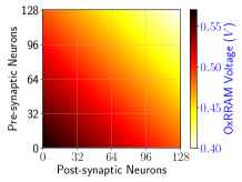
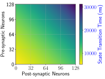
Current variation in a crossbar leads to a difference in the voltage applied across different OxRRAM cells in a crossbar. This is illustrated in Figure 6a, where the minimum and maximum voltages are 0.4 V and 0.57 V, respectively. Such voltage differences cause variation of the state transition time (see Equations 2 & 3). Figure 6b shows such variation for OxRRAM cells in the crossbar, with each cell programmed to the HRS state. The minimum and maximum state transition times are 5,227 ms and 31,214 ms, respectively.
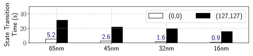
In a recent work, we have shown that the unit parasitic resistance of bitlines/wordlines increases from at 65 nm to at 16 nm [10]. Such increase in the value of parasitic resistance leads to a higher voltage applied across each OxRRAM cell in the crossbar, which further reduces its state transition time. To illustrate this, Figure 7 shows the variation in state transition time of OxRRAM cells in a crossbar at different process technology nodes. We make the following two key observations. First, the state transition time decreases with technology scaling. This is due to an increase in the voltage within the crossbar at scaled nodes. Second, the variation of state transition time increases at smaller nodes due to higher voltage and current variations [10].
Finally, the state transition time of OxRRAM cells also depends on the resistance state. Figure 8 shows the dependence of the minimum state transition time of OxRRAM cells in a crossbar for the four process technology nodes. We make two key observations. First, the state transition time reduces with technology scaling, which we have analyzed before. Second, the state transition time of an OxRRAM cell is higher when the cell is programmed in the HRS state for all process technology nodes. This is because the vertical filament growth phenomena (in HRS state) in OxRRAM technology is slower than the lateral filament growth (in LRS state).

During each inference operation, OxRRAM cells of a crossbar propagate spikes from a machine learning workload. To compute the inference lifetime of an OxRRAM cell, which is defined as the number of inference operations it takes for the resistance state of the cell to drift from its programmed value, we let be the average number of spikes through the cell per inference operation. Formally, inference lifetime is
| (4) |
To ensure integrity of machine learning, i.e., to prevent accuracy drop, the OxRRAM cell must be reprogrammed to the original resistance state once every inference lifetime. Since different OxRRAM cells in a neuromorphic crossbar have different inference lifetime, the reprogramming interval of model parameters to the hardware (see Eq. 1) is defined as the minimum inference lifetime of all OxRRAM cells in the crossbar, i.e.,
| (5) |
The number of spikes propagating through an OxRRAM cell depends on the machine learning workload and how the workload is mapped to the crossbar. This is described next.
IV Workload Dependency of Inference Lifetime
To understand the workload dependency of inference lifetime, we focus on Equation 9. Here, is the average spikes per image through an OxRRAM cell implementing the machine learning workload. This is computed as follows. Consider our machine learning model is represented as with the set of neurons and the set of synapses. If is the number of spikes communicated via from its pre-synaptic to its post-synaptic neuron, then the total number of spikes for the image is . In our implementation, each synapse (i.e., its weight) is programmed on an individual OxRRAM cell. Therefore, the number of spikes through all OxRRAM cells of the hardware is . We compute the average number of spikes per image through an individual OxRRAM cell as the sum of spikes for all images inferred by the model averaged over the number of images and synapses, i.e.,
| (6) |
where is the number of images inferred by .
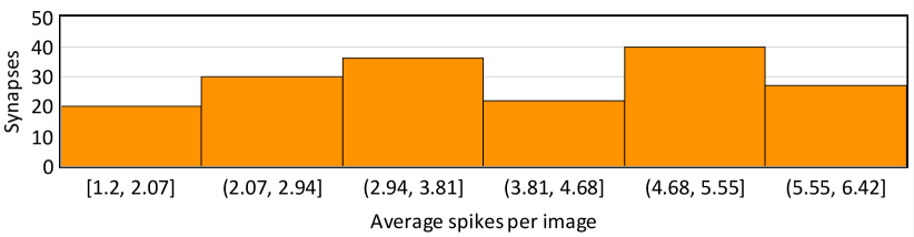
Figure 9 shows the histogram of average spikes per image propagating through the synapses of VGGNet. We collected these statistics by analyzing CIFAR-10 training and test datasets. We see that there are 20 synapses in the model that communicate between 1-2 spikes per image, 30 synapses that communicate between 2-3 spikes per image, and so on. Therefore, some synapses propagate more spikes than others.
If we consider two different synapses of a model with different spike count, then the one with a higher number of spikes will result in a lower inference lifetime when mapped to the OxRRAM cell at a specific position in the crossbar.
Additionally, the spike count on a synapse also depends on the input presented to a model. To illustrate this, Figure 10 plots the spike firing rate of 100 randomly-selected neurons in VGGNet. We observe that the spike firing rate of a neuron in VGGNet depends on the image presented to the model.

The proposed design methodology incorporates such application and model-dependent behavior to better optimize the synapse mapping to OxRRAM cells. This is described next.333The scope of the current work is on design-time approaches in mitigating resistance drift. Our future work will involve designing a run-time framework to evaluate spike count of synapses based on the model input and enable remapping of the synaptic connections to further reduce the system overhead.
V Proposed Design Methodology
Figure 11 shows the proposed system architecture designed in NeuroXplorer [6]. A machine learning model is first trained using training data. The model parameters are stored in memory. The trained model is clustered using the graph partitioning algorithm of NeuroXplorer. For each cluster, an optimization is performed to map the neurons and synapses of the cluster to the OxRRAM cells of a crossbar, by exploiting 1) spike data collected from the training set and 2) technology-specific state-transition time data obtained from characterizing the hardware. The cluster optimization step generates the parameter reprogramming interval , which is then used to periodically reprogram the model parameters to the hardware via bandwidth-limited memory channels. The new blocks that we introduce in NeuroXplorer are shown in red in Fig. 11.

We introduce the following notations to formulate the cluster optimization problem.
| Set of pre-synaptic neurons of a cluster | |||
| Set of post-synaptic neurons of a cluster | |||
| Set of synapses of a cluster | |||
Following are the constraints.
-
•
A pre-synaptic neuron can be mapped to exactly one input port of a crossbar, i.e.,
(7) -
•
A post-synaptic neuron can be mapped to exactly one output port of a crossbar, i.e.,
(8)
We formulate the optimization problem as follows. defines the mapping of synapse to the OxRRAM cell in the crossbar. The inference lifetime of this mapping is
| (9) |
The optimization problem is
| (10) |
The non-linear operation of multiplication of two binary variables and is linearized by introducing a new product variable , with the following additional constraints.
-
•
If and/or , then , i.e.,
(11) -
•
If and , then , i.e.,
(12)
The new optimization problem is
| (13) |
This max-min optimization problem is a convex one (proof of KKT conditions are omitted for space limitations). The problem can be solved using CVXPY by introducing a slack variable as
| (14) |
To incorporate the criticality of a synaptic connection (see Section II), we assign a very small number as the spike count for the synapse. In other words, the spike count of critical synapses is identified using the training set, while those for non-critical synapses are set to a very small value. In this way, we force (see Eq. 9) to a very large value for the non-critical synapses. This allows the convex optimizer to eliminate them from the critical path of determining the reprogramming interval (see Eq. 14).
VI Results and Discussion
We evaluate the proposed design methodology for OxRRAM-based neuromorphic hardware. We configure NeuroXplorer with the hardware parameters listed in Table I.
| Neuron technology | 16nm CMOS (original design is at 14nm FinFET) |
|---|---|
| Synapse technology | HfO2-based OxRRAM [2] |
| Supply voltage | 1.0V |
| Energy per spike | 23.6pJ at 30Hz spike frequency |
| Energy per routing | 3pJ |
| Switch bandwidth | 3.44 G. Events/s |
We use five commonly-used convolutional neural network (CNN) applications with 2-bit quantized synaptic weights. These applications are described in Table II.
| CNN | Dataset | Neurons | Synapses | Avg. Spikes/Image | Accuracy-Full | Accuracy-2 bit |
|---|---|---|---|---|---|---|
| LeNet | CIFAR-10 | 80,271 | 275,110 | 724,565 | 86.3% | 55.4% |
| AlexNet | CIFAR-10 | 127,894 | 3,873,222 | 7,055,109 | 66.4% | 69.5% |
| VGGNet | CIFAR-10 | 448,484 | 22,215,209 | 12,826,673 | 81.4 % | 55.3% |
| ResNet | CIFAR-10 | 266,799 | 5,391,616 | 7,339,322 | 57.4% | 48.0% |
| DenseNet | CIFAR-10 | 365,200 | 11,198,470 | 1,250,976 | 46.3% | 28.2% |
We evaluate the following techniques.
-
•
SpiNeMap. This Baseline approach first clusters a machine-learning inference model to minimize the inter-cluster spike communication [12]. Clusters are then mapped to crossbars of a neuromorphic hardware with synapses of each cluster implemented randomly on OxRRAM cells of a crossbar.
-
•
Endurer. This is our previous work, which addresses the reprogramming of model parameters on crossbars of a neuromorphic hardware to maintain model integrity [5]. A machine learning model is clustered using SpiNeMap. Clusters are placed to crossbars to maximize inference lifetime. To map cluster synapses to the OxRRAM cells of a crossbar, Endurer uses a binary non-linear optimization problem formulation.
-
•
Proposed. The proposed approach is based on Endurer. It introduces the following two new changes to Endurer – 1) it characterizes a machine learning model to identify non-critical synapses such that they could be eliminated from the critical path of determining the reprogramming interval, and 2) the convex optimization formulation and the proposed linearization technique improves the solution quality and improves the speed-up, accelerating the design space exploration.
VI-A Accuracy
Figure 12 reports the accuracy improvement due to periodic reprogramming of model parameters in Endurer and the proposed approach compared to SpiNeMap, where no reprogramming is performed. We observe that by enabling reprogramming of model parameters, model accuracy can be improved by 25% (between 3% and 87%). This is because, without periodic reprogramming in place, model parameters may drift due to frequent accesses of OxRRAM cells where these parameters are programmed. Parameter drift leads to lower accuracy. Additionally, the extent of accuracy impact depends on the specific model that is programmed to the hardware. For AlexNet, we observe a 47% drop, while for ResNet and DenseNet, the drop is only 4%.

VI-B System Overhead
Figure 13 reports the system overhead of the proposed approach compared to Endurer for the evaluated CNNs. Results are normalized to Endurer. Since SpiNeMap does not involve periodic reprogramming, so there is no system overhead. We have therefore not shown SpiNeMap in the figure.

We observe that the system overhead of the proposed approach is on average 35% lower than Endurer (between 23% and 50%). This improvement is due to the increase of reprogramming interval in the proposed approach. Such improvement is attributed to two factors. First, non-critical synapses are not on the critical path for determining the reprogramming interval in the proposed approach, while such synapses are factored in determining in Endurer. Second, the convex optimizer CVXPY of the proposed approach generates a better solution than the approximate binary non-linear optimization technique of Endurer.
We also observe that the improvement is usually higher for models with higher fraction of non-critical synapses. Therefore, the improvement for ResNet is higher than LeNet.
VII Conclusion
In this work, we study the resistance drift related reliability issues in OxRRAM-based neuromorphic hardware used to implement machine learning inference models. Through circuit-level simulations we show the dependence of these issues on 1) the resistance state of an OxRRAM cell (model parameter dependency), 2) the current through the cell (circuit dependency), and 3) the spikes propagating through the cell (workload dependency). We incorporate this study in a system software framework and show a significant accuracy drop due to resistance drift. To maintain the integrity of machine learning inference, model parameters need to be reprogrammed to the hardware periodically, which incurs a significant system overhead. We propose an approach to minimizing this system overhead by first analyzing a machine learning model to identify non-critical synapses, and then proposing a convex optimization solution to maximize the reprogram interval. The proposed optimizer eliminates the non-critical synapses from the critical path of determining the reprogram interval. Evaluations with five commonly-used CNN applications show an average 35% improvement in the system overhead.
Acknowledgment
This work is supported by the National Science Foundation Faculty Early Career Development Award CCF-1942697 (CAREER: Facilitating Dependable Neuromorphic Computing: Vision, Architecture, and Impact on Programmability).
References
- [1] M. L. Varshika et al., “Design of many-core big little Brains for energy-efficient embedded neuromorphic computing,” in DATE, 2022.
- [2] A. Mallik et al., “Design-technology co-optimization for OxRRAM-based synaptic processing unit,” in VLSIT, 2017.
- [3] W. Shim et al., “Impact of read disturb on multilevel RRAM based inference engine: Experiments and model prediction,” in IRPS, 2020.
- [4] V. Milo et al., “Multilevel HfO2-based RRAM devices for low-power neuromorphic networks,” APL Materials, 2019.
- [5] S. Song et al., “Improving inference lifetime of neuromorphic systems via intelligent synapse mapping,” in ASAP, 2021.
- [6] A. Balaji et al., “NeuroXplorer 1.0: An extensible framework for architectural exploration with spiking neural networks,” in ICONS, 2021.
- [7] S. Han et al., “Deep compression: Compressing deep neural networks with pruning, trained quantization and Huffman coding,” arXiv, 2015.
- [8] A. Chaudhuri et al., “Hardware fault tolerance for binary RRAM crossbars,” in ITC, 2019.
- [9] T. Spyrou et al., “Neuron fault tolerance in spiking neural networks,” in DATE, 2021.
- [10] T. Titirsha et al., “Endurance-aware mapping of spiking neural networks to neuromorphic hardware,” TPDS, 2021.
- [11] A. Paul et al., “Design technology co-optimization for neuromorphic computing,” in IGSC Workshops, 2021.
- [12] A. Balaji et al., “Mapping spiking neural networks to neuromorphic hardware,” TVLSI, 2020.
| Ankita Paul Ankita Paul is currently pursuing a Ph.D. degree from Drexel University under the supervision of Dr. Anup Das. She received a Bachelor’s degree from West Bengal University of Technology in 2016. Her research interests include brain inspired computing, deep learning, and machine learning. |
| Shihao Song Shihao Song is currently pursuing a Ph.D. degree from Drexel University under the supervision of Dr. Anup Das. He received a Bachelor’s degree from Drexel University in 2017. His research interests include computer architecture, non-volatile memory, and compiler design for neuromorphic hardware and accelerators. |
| Twisha Titirsha Twisha Titirsha is currently pursuing a Ph.D. degree from the Department of Electrical and Computer Engineering, Drexel University, Philadelphia. She received a Bachelor’s degree from Military Institute of Science and Technology, Bangladesh in 2015. Her research interests include computer architecture, non-volatile memory and mixed-signal circuit design. |
| Anup Das Dr. Anup Das is an Assistant Professor at Drexel University. He received a Ph.D. in Embedded Systems from National University of Singapore in 2014. Following his Ph.D., he was a post-doctoral fellow at the University of Southampton and a researcher at IMEC. His research focuses on neuromorphic computing and architectural exploration. He is a senior member of the IEEE. |