Nonlinearity and wavelength control in ultrashort-pulse subsurface material processing
Abstract
The pronounced dependence of the nonlinear parameters of both dielectric and semiconductor materials on the wavelength, and the nonlinear interaction between the ultra-short laser pulse and the material requires precise control of the wavelength of the pulse, in addition to the precise control of the pulse energy, pulse duration and focusing optics. This becomes particularly important for fine sub-wavelength single pulse sub-surface processing. Based on two different numerical models and taking \ceSi as example material, we investigate the spatio-temporal behavior of a pulse propagating through the material while covering a broad range of parameters. The wavelength-dependence of material processing depends on the different contributions of two- and tree-photon absorption in combination with the Kerr effect which results in a particularly sharp nonlinear peak at . We could show that in silicon this makes processing preferable close to this wavelength. The impact of the nonlinear nonparaxial propagation effects on spatio-temporal beam structure is also investigated. It could be shown that with increasing wavelength and large focusing angles the aberrations at the focal spot can be reduced, and thereby cleaner and more precise processing can be achieved. Finally, we could show that the optimum energy transfer from the pulse to the material is within a narrow window of pulse durations between .
I Introduction & State of the Art
Fine material processing of semiconductors in general, and silicon in particular is a hot topic both in the scientific community as well as in industry. Up to now a lot of effort has been put into surface processing experiments using mainly nanosecond pulse durations and pulse energies above [1, 2, 3, 4, 5, 6, 7, 8]. Processing technology has been well understood both on the practical and theoretical level [9, 7]. In the last few years the focus has been shifted towards the next level fine material processing – in particular sub-surface modification of the crystalline silicon using ultra-short pulsed lasers (pico- and femtosecond) at the wavelengths above , where silicon becomes transparent. Several successful studies have been carried out since then [10, 11, 12, 13, 14, 15, 16, 17, 18, 19, 20]. Those sub-surface defects are targeted for such important industrial processes as thin wafer exfoliation [21], sub-surface structuring [17, 21], data storage [22], waveguides [4, 22, 23, 24] and grating fabrication [6]. The common way to introduce sub-surface modifications in all these works is using multiple pulses and pulse trains [25]. Very recently it was shown that also single pulse processing of monocrystalline silicon is possible with ultra-short pulses at , producing particularly fine sub-wavelength modifications [26]. Besides optimization of the laser pulse parameters, the choice of the laser wavelength played a crucial role in this work, suggesting a much more complex nonlinear light-matter interaction with spatio-temporal dynamics that strongly depend on the wavelength. The latter is a subject of the present numerical investigation.
Besides nonlinear multi-photon absorption light propagating through the material experiences several different processes, such as self-focusing [16, 21] and plasma-induced de-focusing and reflection [11, 15], to name a few. Those processes strongly depend on the wavelength and intensity of the pulse propagating through the material [27, 28]. Depending on the wavelength the impact of each parameter will vary. Here, especially the self-focusing effect due to the third-order nonlinearity has to be mentioned, as it becomes extremely strong within a rather narrow wavelength range at a certain wavelength, that depends on the forbidden band-gap of the material. An investigation of the wavelength-dependent interplay of several nonlinear optical effects and their impact on the spatio-temporal dynamics of ultra-short laser-pulses inside the material becomes particularly important for single-pulse sub-surface processing of any material, not only silicon. In the present work we for the for the first time perform such study using silicon as a model.
In silicon the third-order nonlinearity peaks between [27, 28], and therefore influences the pulse significantly stronger than at shorter or longer wavelengths. Within the same wavelength range the two- and three-photon absorption experiences a minimum at this wavelength, thus allowing to reduce the potential for surface damage (due to lower multi-photon absorption) while retaining the capability of delivering a large amount of energy to the focal spot [16]. This makes it possible to achieve pulse beam collapse and correspondingly high intensities at relatively low pulse energies. For certain parameters this might decrease the material processing threshold, while simultaneously increase the precision at which the material can be processed. In Ref. [21] we for the first time suggested to use the interplay of all these nonlinear optical effects to find an optimum wavelength for processing of silicon with - and -pulses. The modelling and experimental results were obtained at low NA values of , and it became clear that using a large focusing angle is necessary to avoid nonlinear absorption too close to the surface, as also mentioned by Zavedeev et al. [15].
In earlier theoretical works Zavedeev et al. [11, 15] it was shown that for a numerical aperture of and a pulse duration of the maximum deposited energy density reaches its maximum value at around and then, after dropping down, starts to grow with the wavelength again. This is in contrast with the maximum plasma density, which decreases with nearly monotonically. Moreover, Kononenko et al. [29] showed that an increase of the pulse energy not necessarily will increase the intensity at the focal spot due to multi-photon absorption, plasma defocusing and reflection. All this suggested the need of careful control of the laser parameters, including wavelength, to make use of the strong wavelength dependence of the material nonlinearity, to achieve a particularly precise single pulse shot processing.
Besides the wavelength, energy and pulse duration are equally important, as experimentally shown by Das et al. [18], Mareev et al. [19]. They demonstrate that a certain pulse duration is necessary to create sub-surface modifications within \ceSi depending on the focusing angle. Das et al. [18] gives a minimum pulse duration of for a focusing numerical aperture of to induce modifications within \ceSi when operating a laser at . For pulses between no increase of the modification threshold could be found [18], except when increasing the pulse duration to nanoseconds. For shorter pulse durations in the femtosecond range Mareev et al. [19] could show a decreasing amount of generated free carriers [19] when keeping the wavelength, pulse energy and focusing optics constant, indicating higher losses while propagating through \ceSi for shorter pulse durations. This was experimentally confirmed by Chambonneau et al. [30].
To the best of our knowledge Zavedeev et al. [15] was the first to have investigated numerically the behavior of femto-second pulses propagating through \ceSi at wavelengths . They stated that the pre-focal depletion of the pulse energy decreases significantly with wavelength, and that the maximum deposited energy density and the plasma defocusing decreases. The decrease in the free-carrier concentration does not cause a similar decrease in the density of the deposited energy, because the inverse bremsstrahlung absorption becomes stronger with longer wavelengths. In spite of all these advantages of going to longer wavelengths they did not expect a significant improvement in femto-second laser processing when going above wavelength at an NA of .
In the last few years large progress has been achieved in development of ultrashort pulsed high energy lasers operating above . Three laser systems could be of potential interest in this wavelength region: a picosecond-fiber \ceHo:MOPA laser, operating at up to at repetition rates [21], a femtosecond \ceCr:ZnS [31] or \ceCr:ZnSe laser with up to pulse energy [32, 33, 34], and an \ceEr:ZBLAN fiber laser operating around , delivering pulse durations down to [35, 36, 37]. The availability of commercial lasers in this wavelength range calls for a detailed numerical analysis that might be particularly important for practical applications of these lasers.
I.1 Mechanisms of sub-surface modifications in silicon
Several mechanism for the modification of the crystal structure of silicon under irradiation with short and ultra-short pulses have already been described. Depending on the pulse parameters and the chosen model each approach relies on different mechanisms, time scales and different thresholds. Below the most relevant approaches for the investigated pulse parameter range are given:
-
1.
So-called “non-thermal melting” is proposed when irradiating silicon with ultra-short pulses [38, 39, 40, 41, 42, 43, 44]. By exciting more than of the valence electrons in the conductance band, corresponding to a plasma density of ) the bonds between the atoms are weakened enough to enable a process which resembles melting, but without reaching the lattice temperatures associated with melting. This process is independent of the wavelength, after it only relies on the density of excited electrons.
-
2.
Following Du et al. [45], B.C et al. [46], Du et al. [47], Tien et al. [48], Chimier et al. [49] reaching the critical plasma density in a material, defined as is sufficient for reaching the modification/damage threshold in a material. This criterion is wavelength-dependent, and scales with . Therefore, it is easier to reach the modification threshold with this definition using longer wavelengths compared to shorter wavelengths.
-
3.
Following Chimier et al. [49], Zhokhov and Zheltikov [50], Werner et al. [51], Chambonneau et al. [7] reaching the threshold given in point 2 is necessary for modifying the material, but not necessarily sufficient. Instead, they propose to relate to the deposited energy within the material when determining if the material will be modified. For ultra-short pulses it can be assumed that the energy initially is retained only within the electrons during the full pulse duration, and only afterwards will be transferred into the lattice. Therefore, as upper limit for the absorbed energy Equation 1 can be used.
(1) Here, gives the band gap, and the generated free-carrier density. Other approaches for determining the threshold (such as the Gamaly-model [52]) are described by Werner et al. [51].
I.2 Applied methods and procedure
In this work we focus on the theoretical study of the spatio-temporal effects of the propagation of the ultra-short pulses inside silicon at different wavelengths above . These effects are a result of the interplay of nonlinear optical effects and have a strong wavelength dependence.
To numerically investigate numerical apertures above a non-paraxial pulse propagation method has to be used, the paraxial approximation is not sufficient for numerical apertures larger than that [53]. For this purpose two different methods are used in this paper, the unidirectional pulse propagation [54] and the generalized Helmholtz equation [55]. While the former approach is a spectral technique using the Fourier split-step method for time stepping, the latter is a purely temporal technique, and is implemented and solved with a finite-element-method (FEM). This allows the generalized Helmholtz approach to better resolve spatial effects at the cost of neglecting spectral effects.
We use numerical simulations to investigate the influence of the wavelength dependence of nonlinear absorption, self-focusing and plasma-related effects for wavelengths between for pulse durations between and compare the influence of the numerical aperture. Moreover, we also investigate the spatio-temporal behaviour of the pulse and demonstrate the significant influence of the generated plasma on the pulse shape while propagating through the material, and at the focal spot.
We apply the methods of the spatio-temporal structure and dynamics control in the nonlinear media under the condition of strong field localization. Our observations demonstrate a possibility of spatio-temporal control like the nonlinear mode-self-cleaning in the multimode fibers [56, 57] that bridges nonlinear fiber- and solid-state laser photonics. Manipulation with highly concentrated spatio-temporal patterns provides the tools for high-energy physics and technology in photonics, information processing, condensed matter modification and others.
II Numerical model and physical parameters
II.1 Physical nonlinear parameters
A light pulse propagating through Silicon is influenced by several different wavelength-dependent nonlinear phenomena, such as the Kerr-effect, multi-photon absorption or plasma absorption and -defocusing.
Within the investigated wavelength range (between and ) only two- and three-photon absorption can be seen as relevant, after single-photon absorption can be neglected for wavelengths above , and four-photon absorption can be neglected for wavelengths below . A graph displaying the values for the two-photon absorption (based on Bristow et al. [58] is shown in Figure 1 in the upper figure in blue, and the values for the three-photon absorption (based on Pearl et al. [59]) are shown in the same figure in orange.
tikztikz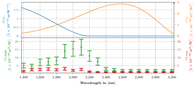
The exact values for the wavelengths (as given in Section II) investigated in this paper are shown in Table 1, together with the corresponding sources.
| Wavelength |
|
|
|
|
|
|||||||||||||
|---|---|---|---|---|---|---|---|---|---|---|---|---|---|---|---|---|---|---|
The strength of the Kerr-effect can vary depending on the doping and orientation of the silicon wafer, and therefore we chose to include two different values as an upper and lower boundary. The wavelength-dependent values are shown in the lower figure in Figure 1 for low -values (based on Lin et al. [27]) in red and in green for high -values (based on Wang et al. [28]). The main difference between the used materials in Lin et al. [27], Wang et al. [28] is the different doping of the material, which in turn results in a different nonlinear refractive index. Wang et al. [28] uses a p-doped material with a doping concentration of , which corresponds to a surface resistivity of . Lin et al. [27] uses a similar p-doped crystal, but with a surface resistivity of , which corresponds to a dopant concentration of . Therefore, a lower dopant concentration in a p-doped crystal corresponds to a lower nonlinear refractive index.
Those parameters can be combined in the so-called Nonlinear Figure of Merit (NFOM). It usually is defined as the relative merit of the Kerr nonlinearity versus the two-photon nonlinearity by the ratio of both values, divided by the optical wavelength in vacuum, according to Mizrahi et al. [62]. When extending this ratio to multi-photon absorption, one obtains the NFoM in the following form [28]:
| (2) |
with the wavelength in vacuum, the wavelength-dependent nonlinear refractive index, the field intensity and the coefficient for -photon absorption.
As shown in Figure 1 it has to be kept in mind that the three-photon absorption coefficient does not decrease to zero for wavelengths below . It still can influence the laser light, provided a certain intensity is reached. This intensity can be determined by comparing the contribution of both two- and three-photon absorption and setting
| (3) |
For this threshold is reached at , while for the threshold can be calculated to be , and thus significantly lower. When no absorption is intended (such as in waveguides) the intensity typically stays below [63], and therefore three-photon absorption can be neglected for shorter wavelengths. For those intensities Equation 2 therefore stays valid.
For processing the absorption, on the contrary, the localized absorption of laser pulses is the main aim, and therefore the intensities will be much higher at least close to the focal spot. At those intensities three-photon absorption will still be an important factor at wavelengths shorter than , and therefore we propose a revised approach for the nonlinear figure of merit for large intensities:
| (4) |
Similarly to three-photon absorption higher-order absorption processes will be present at shorter wavelengths, too. Therefore, it can be beneficial to verify if those processes have to be included in the revised nonlinear figure of merit, and potentially forming the following definition:
| (5) |
The calculation of the threshold intensity at which higher-order multi-photon coefficients will be of interest is complicated by sparse availability of measurement data for higher-order absorption coefficients in \ceSi over a large range of wavelengths. Gai et al. [60] provides several measurement points for the four-, five- and six-photon absorption coefficients, but only within a limited wavelength range (unlike the data given for the three-photon absorption coefficient). The lowest wavelength where the four-photon absorption coefficient has been measured is [60], with a value of . Compared to the three-photon absorption coefficients at and a threshold intensity can be calculated (by following Equation 3) at . Together with the decrease of the four-photon absorption coefficient for shorter wavelengths (i.e. ) it therefore can be safely assumed that for intensities below and above Equation 4 can be used, and replaces Equation 2 as the definition of the nonlinear figure of merit. Graphs based on Equations 2 and 4 showing the change of the nonlinear figure of merit for increasing intensities are given in Figure 2. Following the estimations made above the transition from Equation 2 to Equation 4 is at . The values for the nonlinear figure of merit depending on the intensity and wavelength are shown in Figure 2, with a cross-section at shown in Figure 3. It has a clearly visible peak at due to the transition from two-photon absorption to three-photon absorption combined with the maximal Kerr-effect contribution.
tikztikz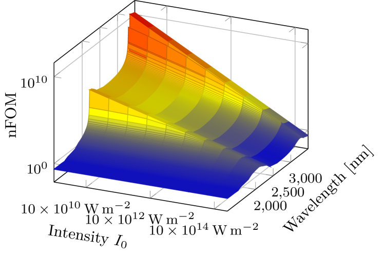
tikztikz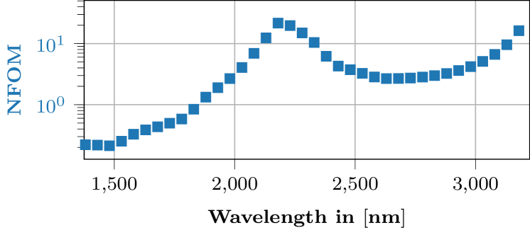
In Figure 2 it can be seen that the three-photon absorption combined with the intensity gradually increases, which shifts the peak of the nonlinear figure of merit towards the shorter wavelengths (up to for ) while simultaneously lowering the whole nonlinear figure of merit. This indicates the growing importance of higher-order absorption compared to lower-order absorption due to the scaling with the intensity, a relation which also is displayed in Figure 4.
II.2 Numerical model and methods
To model the propagation of the pulse through Silicon we use the scalar unidirectional pulse propagation equation (UPPE) [54, 64], written as
| (6) |
with the Fourier-transformed electric field of the pulse, the (non-)linear polarizations acting on the pulse and the (non-)linear current densities acting on the propagating pulse. The wave number is given by and the propagation constant in a cylindrical coordinate system is defined as (based on Couairon et al. [65], Fedorov et al. [53])
| (7) |
to allow the calculation of tightly focusing optics with an NA while still using a scalar equation.
The main advantage of the UPPE compared to the nonlinear Schrödinger equation (NLSE) for simulating the nonlinear propagation of a light pulse in Silicon is the inclusion of non-paraxial effects. This allows the numerical simulation of optics with a very large numerical aperture.
One has to note, that Equations 6 and 7 correspond to the generalised Helmholtz equation written in a co-moving coordinate system ( is a local time, is a time in the laboratory coordinate system, is a group velocity of a pulse, and is a radial coordinate within the axial symmetry approximation) [55]:
| (8) |
The transverse Laplacian in Equation 8 reads as , where is a radial coordinate.
The contribution to the nonlinear polarization corresponds to that represented by the terms in eq. 6. That are defined by the Kerr-effect, described in section II.1, while the nonlinear multi-photon absorption (two- and three-photon absorption) and the plasma absorption and -defocusing are part of the nonlinear currents.
The UPPE-equation (c.f. Equations 6 and 7) is a very effective tool for simulations of field dynamics outside the paraxial approximation. Using the split-step Fourier approach could promise an acceleration of computation. However, the interweaving of spatial and space degrees of freedom requires the evaluation of big-size matrices, which is a memory-intensive task. The generalized Helmholtz-equation (Equation 8) is evaluated based on the finite element method (FEM) in the time domain. The advantage of this technique is its applicability to complicated geometrical structures, the possibility of using a broad class of very effective numerical solvers, and the adaption of the simulation mesh which can accelerate calculations substantially. Both methods are based on the same equation set and are complementary. Their preferable use depends on the conditions of strongly unsteady-state dynamics [66, 67]. Nevertheless, one has to note that FEM allows adopting the mesh to a concrete field configuration changing with propagation and, thereby, accelerating the calculations substantially. In this paper we used both methods to make use of the best complementarity of both approaches, and maximum efficiency of numerical calculations.
Finally, the generation of free carriers is describes by using (from Couairon et al. [64])
| (9) |
The rate equation contains the free carriers generated due to nonlinear absorption, defined as
| (10) |
with the number of involved photons, and the free carriers generated due to avalanche ionization, defined as
| (11) |
Here, the inverse Bremsstrahlung coefficient is defined as
| (12) |
The intensity is defined as , and is the band gap energy. in Equation 12 is the electron collision time. Finally, in Equation 10 is given as
| (13) |
with the neutral free carrier density.
We decided to neglect the recombination rate of the generated free carriers due to their long lifetime, up to [68], which is significantly longer than the pulse duration.
Equation 6 was implemented while using functions from the libraries deal.II [69, 70] and PETSc [71, 72]. The computations were run on the local HPC cluster IDUN/EPIC [73] and on resources provided by UNINETT Sigma2 – the National Infrastructure for High Performance Computing and Data Storage in Norway.
III Numerical simulations
Initial investigations of the wavelength dependence of the pulse propagation in silicon was already done before, as for example by Richter et al. [16, 21, 74], but those investigations were limited by the used method for numerical simulations. Richter et al. [16, 21] used the NLSE for simulating the pulse propagation, which limits the maximum focusing angle which can be used. On the other hand Das et al. [18] reported experimentally for that an NA value of has to be used for pulse durations of , which limits the applicability of the NLSE for those pulse durations. Nevertheless, at least for lower focusing angles it could be shown that between the efficiency of the energy delivery to the focal spot was increased compared to longer and shorter wavelengths.
To investigate and correlate the experimentally observed behavior with numerical simulations we chose to simulate a pulse at four different wavelengths, , , and with the pulse energies ranging from to . A full overview over all parameters is given in Table 2. Here, the maximum pulse energy for an NA of is , while the maximum pulse energy for an NA of is .
| Parameter | Value | Unit | ||
|---|---|---|---|---|
| Pulse duration | , , , | |||
| Pulse wavelength |
|
|||
| Pulse energy |
|
|||
|
, , | |||
|
1 | |||
| Focus depth | , , , |
For all calculations with the UPPE the initial beam diameter was set to for a wavelength of . To achieve a similar fluence in the focal spot for linear propagation, the beam radius for other wavelengths was adjusted using
| (14) |
unless explicitly noted otherwise.
While this will result in a similar fluence level at the focal spot independently of the wavelength, it will result in changed focusing angles. This in turn will influence the impact of the nonlinear effects onto the propagation of the pulse. A smaller NA value will result in a higher intensity closer to the surface of the material, and thereby triggering self-focusing and nonlinear absorption earlier compared to larger focusing angles. The used NA-values corresponding to each wavelength are listed in Table 3.
| Wavelength | Target NA: | Target NA: |
|---|---|---|
| 0.25 | 0.85 | |
| 0.31 | 1.07 | |
| 0.35 | 1.18 | |
| 0.41 | 1.40 | |
| 0.52 | 1.78 |
The numerical apertures used for the HHE are listed in Table 4, in comparison.
| Wavelength | Numerical aperture | Figure |
|---|---|---|
| Figures 6 and 10 | ||
| Figure 5 | ||
| , | Figure 12 |
III.1 Impact of the intensity on the absorption
The multi-photon absorption coefficients of order shown in Figure 1 contribute to the current density as defined in Equation 6 via
| (15) |
with the refractive index, the absorption coefficient of -photon absorption and the intensity. While the absorption due to free carriers does scale with the wavelength, but not with the intensity, and therefore is not included in this discussion. Combining Equation 15 with Table 1 the generated current can be calculated, which is displayed in Figure 4, and will be shortly elaborated in Section III.1.
tikztikz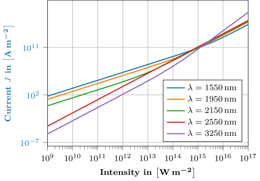
As displayed in this figure the total absorption due to multi-photon absorption scales with the intensity. Depending on the order of the multi-photon absorption this scaling factor is either purely , or a combination of both. A higher scaling factor can lead to a higher absorption current, even though the absorption coefficient itself is lower. This effect can be seen especially for . While the generated current for an intensity of is five orders of magnitude lower than the current generated by , it is equal for an intensity of , and higher than that for increasing intensities. These intensities are roughly comparable to the intensities reached by a pulse with an energy of and a duration of at a wavelength of , focused with a lens with and a beam diameter of . This gives a focal spot area of , and with a peak power (for a Gaussian pulse) of the peak intensity is , i.e. an intensity which can be easily achieved.
Similarly, the transition intensity for the shorter wavelengths can be taken from Figure 4, and can be approximated to be , corresponding to a pulse with and the parameters used above. Nevertheless, one has to keep in mind that the intensity at the focal spot was taken into account here. When focusing deep into the material the affected area increases, which in turn decreases the intensity. Setting the focal depth to in \ceSi, corresponding to in air, will increase the affected area by a factor of , and reduce the intensity accordingly. Decreasing the focal length of the lens (and thereby increasing the numerical aperture) will affect the intensity. Going from an NA of as used above to an NA of (which is typically used for processing experiments [21, 18]) by decreasing from to will increase the affected area by and lower the intensity accordingly. This is especially important for longer wavelengths, after the total absorption for higher-order multi-photon absorption processes scales faster with the intensity.
III.2 Influence of the non-paraxiality on the pulse shape
To demonstrate the importance of using methods which do not rely on the paraxial approximation for propagating the laser pulse a pulse was simulated using Equation 8, once while including the paraxial approximation, and once without, while keeping the pulse parameters constant. The pulse structure at the same position within silicon is shown in Figure 5(a) for the case of included paraxial approximation, and in Figure 5(b) for the case without approximation.
tikztikz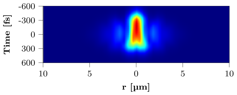

tikztikz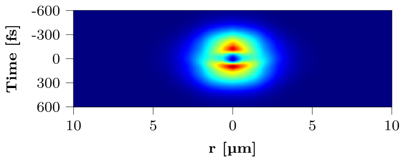

In comparison a clear difference is visible. While the paraxial approach results in an elongated structure, the non-paraxial approach shows a clear intensity dip in the center of the pulse. Despite a relatively small NA Figure 5, the non-paraxial approximation addresses more precisely the nonlinear factors causing the spatial-time reshaping of a beam.
III.3 Spatio-temporal structure and impact of spherical aberrations
While propagating through the material the pulse changes its shape both in space and in time. This is visualized in Figures 7(a), 7(b), 7(c) and 8(a). These figures demonstrate the spatio-temporal evolution of a light pulse with , and a wavelength of , focused into \ceSi with a lens with . The focal spot was placed at in air, corresponding to in \ceSi due to the increased refractive index.
Simulations based on both Equations 6 and 8 demonstrate the appearance of spherical aberrations (c.f. Figure 6(a)). A spatial substructure appears in the form of “light rings”, which evolves to and squeezes with a distance due to self-focusing (c.f. Figure 6(b)).
tikztikz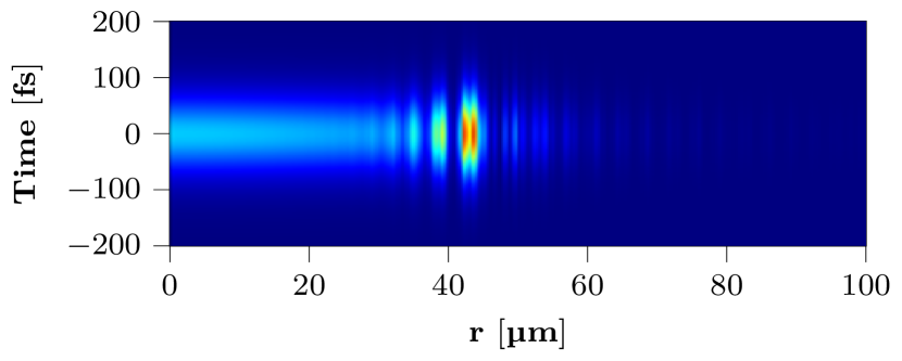

tikztikz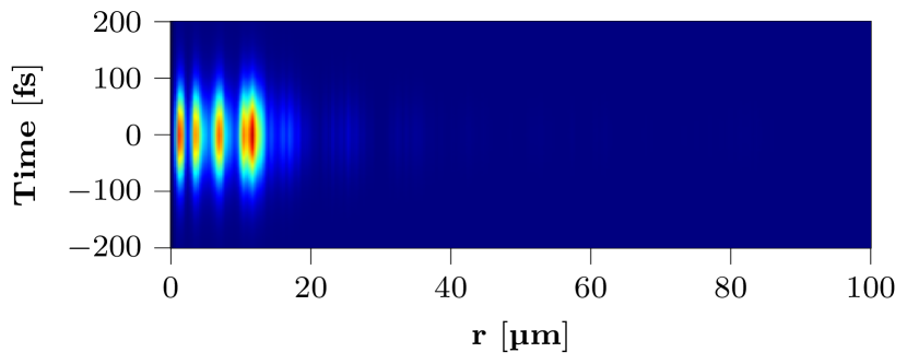

pngtikz
pngtikz
pngtikz
pngtikz
Several points can be noted about the pulse behavior already before the focal spot. Going from (Figure 7(a)) to (Figure 7(b)) not only the pulse in total is focused towards the focal spot, but also the effect of self-focusing is visible. The innermost part of the pulse with the highest intensity is focused more compared to the rest of the pulse, creating an asymmetric shape along the spatial axis. Nevertheless, the pulse stays symmetric along the time axis.
This effect can be considered as analogue to the Kerr-beam self-cleaning in multi-mode fibers, as demonstrated by Krupa et al. [57]. The calculations demonstrate that the NA growth enhances the tendency for generating multiple rings. Still, this effect degrades quickly at the wavelength close to the maximum of NFOM and longer wavelengths.
Shortly before the focusing point, though, the self-focusing effect together with the generated plasma leads to a deformation of the beam not only in space, but also in time. As also shown below in Figures 16(a), 16(b), 17(a) and 17(b), the leading part of the pulse generates a large amount of free carriers, which lead to diffraction and multi-photon absorption. Due to the multi-photon absorption scaling nonlinearly with the intensity this affects the central part of the pulse dis-proportionally more compared to the leading and trailing edge. Generated free carriers also lead to absorption, but only linearly, and therefore can be neglected for high intensities. Still, for a sufficient density the absorption due to free carriers is visible, and can be seen for the trailing part of the pulse in Figures 7(c) and 8(a). For this part the intensity is reduced by compared to the leading edge.
Figure 5, based on Equation 8, demonstrates the effect of time asymmetry in the vicinity of the first maximum of the NFOM (c.f. Figures 2 and 3) at . This effect is connected with the plasma generated by the pulse front that initiates the pulse “explosion” (c.f. Figure 10).
pngtikz
pngtikz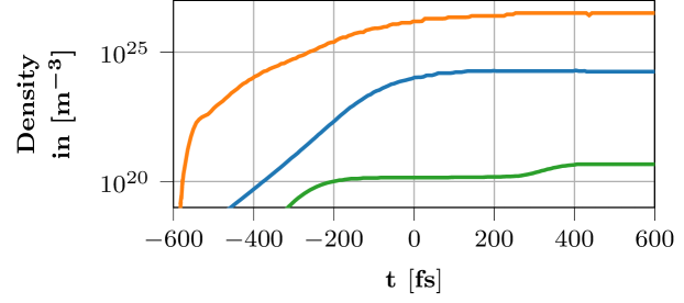

pngtikz
pngtikz
III.4 Impact of the numerical aperture (NA) and focusing depth on the nonlinear pulse propagation
Changing the physical position of the lens itself (i.e. shifting the depth of the focal spot inside the material) and the parameters of the lens itself (i.e. changing the numerical aperture) influences how the beam propagates inside the material, and how the different nonlinear material parameters can act on the propagating beam. For a varying depth and a fixed numerical aperture the difference is visible for a numerical aperture of , as shown in Figure 11.
tikztikz
tikztikz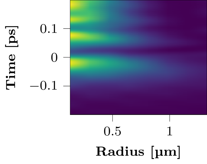
tikztikz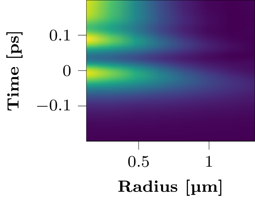
tikztikz
tikztikz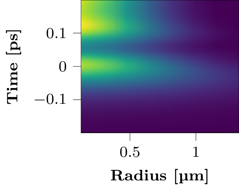
tikztikz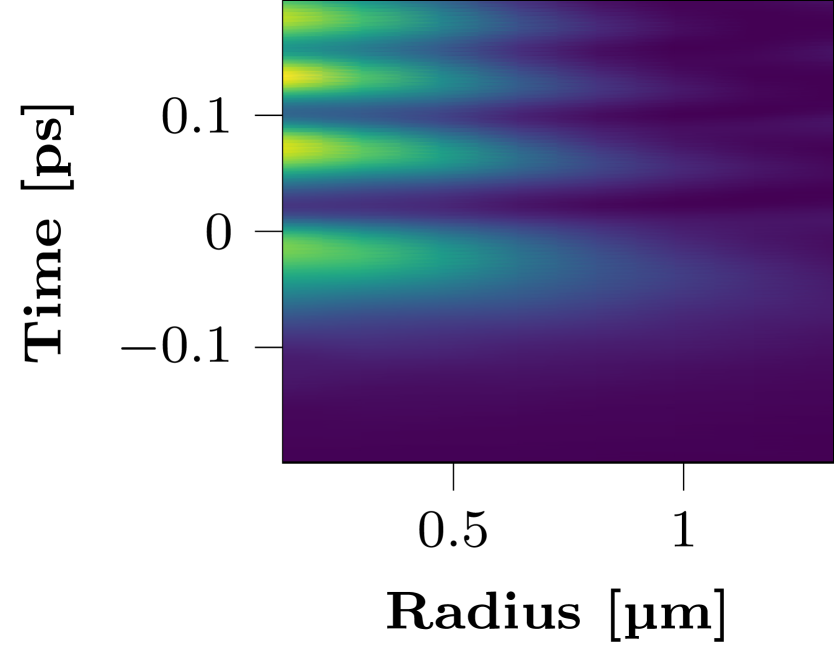
tikztikz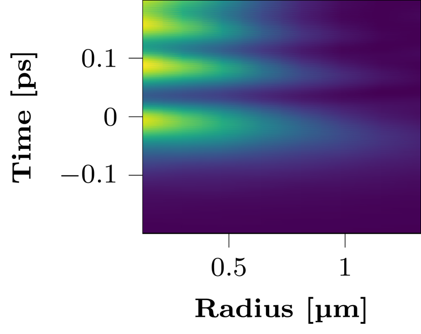
tikztikz
tikztikz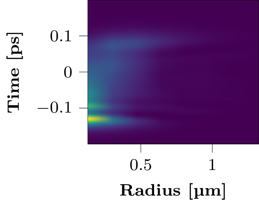
tikztikz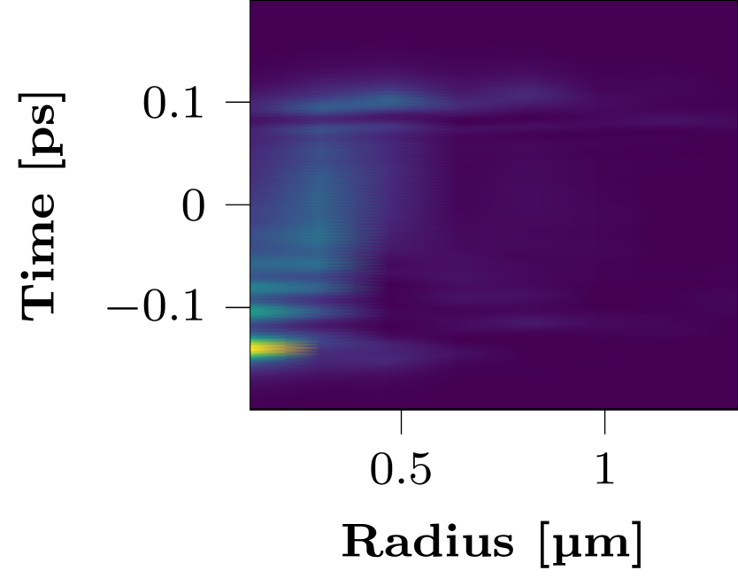
tikztikz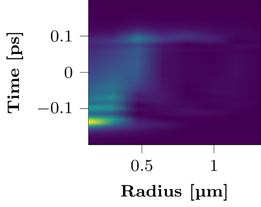
tikztikz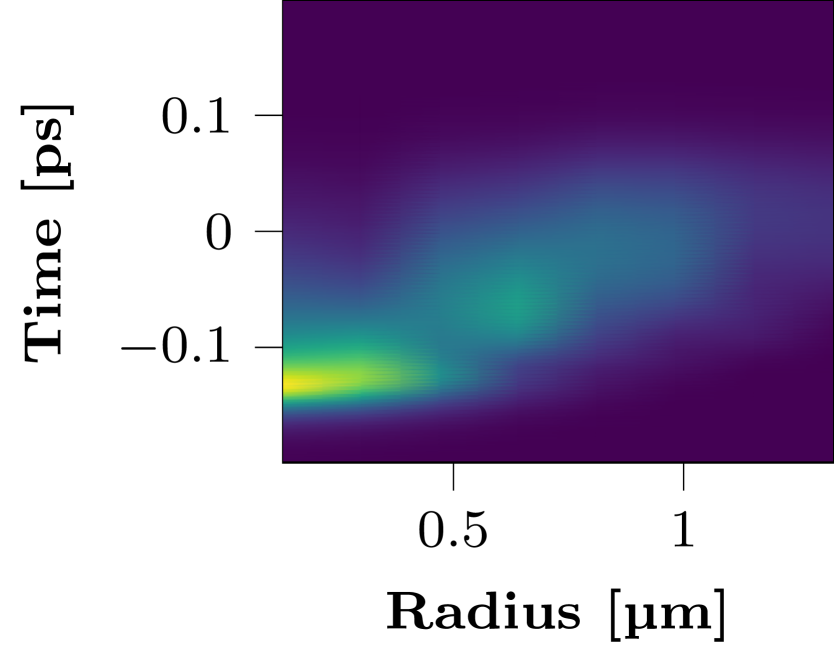
Moving the focal spot deeper into the material will change the intensity distribution along the propagation path, such that nonlinear effects, especially self-focusing, can act on the beam for a longer period, and therefore change the resulting intensity field distribution at the focal spot. This behavior is visible especially for , after those wavelengths experience a stronger self-focusing compared to shorter and longer wavelengths (as shown in Figure 1). This effect is visible especially along the beam propagation axis, as shown in Figure 17.
When increasing the numerical aperture from to the initial intensity along the propagation path is lower, and therefore nonlinear effects will start closer to the focal spot. Therefore, almost no difference is visible in the structure of the intensity field distribution for an NA of is visible (c.f. Figures 17(a) and 17(b)), while the pulse focused with a lower NA value changes its structure when changing the focal depth. This demonstrates that larger focusing angles are necessary for processing closer to the surface, where the interaction length with nonlinear effects will be reduced around the focal spot compared to lower focusing angles.
III.5 Spatio-temporal pulse behavior depending on pulse wavelength and -energy
tikztikz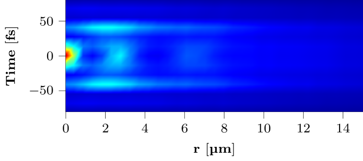

tikztikz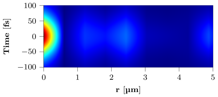

The spatio-temporal splitting described in Section III.3 and shown in Figures 7(a), 7(b), 7(c) and 8(a) does depend on several different factors such as pulse wavelength, pulse energy, pulse duration and the focusing optics. While the first parameter influences the value of the material parameters (as seen in Table 1), the latter three influence how the intensity of the pulse will behave while travelling through the material. A higher intensity will result in both earlier self-focusing and a faster onset of multi-photon absorption, which in turn are both influenced by the value of the material parameters set by the wavelength. As a first comparison the intensity of a pulse with and is shown in Figures 11(i), 11(j), 11(k) and 11(l), when focused with a target NA of (ref. Table 3) and the focus point set to below the surface of \ceSi. In addition to the spatio-temporal representation of the field shown in Figures 11(i), 11(j), 11(k) and 11(l) corresponding slices taken at for both the temporal intensity and the generated free carrier density are shown in Figures 18(b) and 17(a) for a focus depth of and in Figures 18(d) and 17(b) for a focus depth of .
The effect of multi-photon absorption and plasma diffraction can clearly be seen for all pulse wavelengths. The trailing part of the pulse has been absorbed almost completely, resulting in a shift of the peak intensity towards the leading edge. In addition the self-focusing effect introduces oscillations, especially for and .
Here, it is also worth to mention the intensity distribution over the wavelengths at the focal spot. For the linear propagation without absorption or diffraction the intensities should be equal at the focal spot, but even though the self-focusing effect is stronger at and compared to the shorter and longer wavelengths, the peak intensity follows the absorption curve shown in Figure 4 at , with the shortest wavelength having the highest peak intensity. Nevertheless, the difference between the peak intensities is negligible, with the peak intensity at only times smaller than the peak intensity at . In comparison to this difference in intensity the density of the generated free carriers is roughly comparable for all wavelengths independently of the depth of the focus point (as shown in Figures 18(b) and 18(d)), with the generated density being slightly higher for by . This indicates that the absorbed energy going into the generation of free carriers is roughly the same, independently of the wavelength.
In comparison to a lens with an NA of one also notices that the field is longer in time (especially visible in the slices shown in Figures 17(a), 17(b), 16(a) and 16(b)). For a numerical aperture of the pulse is stretched to over , while for a numerical aperture of the pulse is only stretched to , depending on the observed wavelength, and thereby much closer to the original pulse duration.
For long wavelengths, the spherical aberrations decay so that a field concentrates in a comparatively symmetrical spot at some propagation distance inside a medium (see Figure 12). As one can see from Figures 1 and 2, the two-photon absorption process decreases towards this wavelength range so that a relative contribution of the Kerr-effect increases. Thus, a plasma influence on a beam focusing destabilization and a damage threshold decays. As a result, a non-destructive modification of material becomes possible. One must note that the weakening of plasma contribution breaks the spatial-time relation mentioned above. Namely, a beam squeezes mainly in spatial dimension than in the time one for the large NA (compare Figure 12). Our analysis demonstrates that such an effect could cause a spatial-time splitting at some propagation distances, which requires control of initial beam parameters.
III.6 Correlation between the pulse duration, the pulse wavelength, the pulse energy and the peak intensity/peak free carrier density/absorbed energy
As shown in Figure 4 the absorption of the pulse largely depends on the pulse intensity. To reduce the intensity of the pulse there are several options: Increasing the focal spot size, decreasing the pulse energy or increasing the pulse duration. With the size of the modifications in \ceSi as the main goal the first option is not ideal, and therefore either the pulse energy has to be decreased, or the pulse duration increased. The effectiveness of both approaches is compared in Figure 13.
tikztikz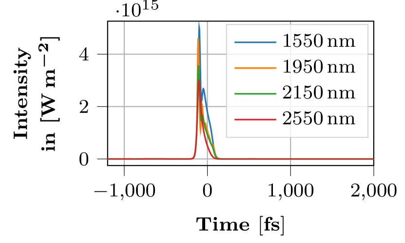
tikztikz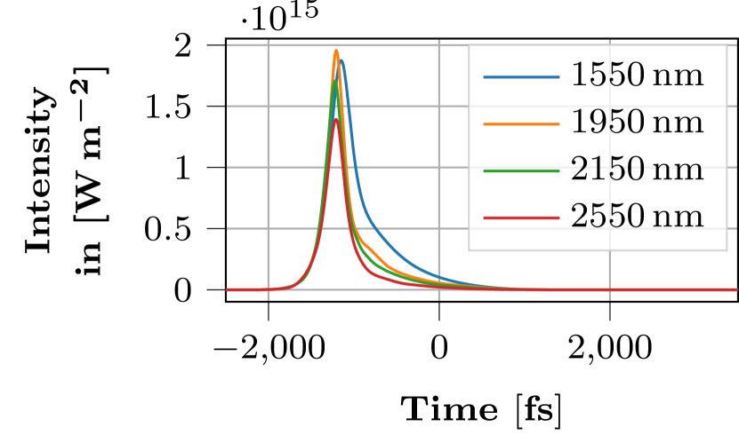
tikztikz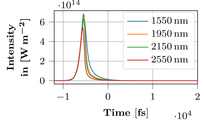
tikztikz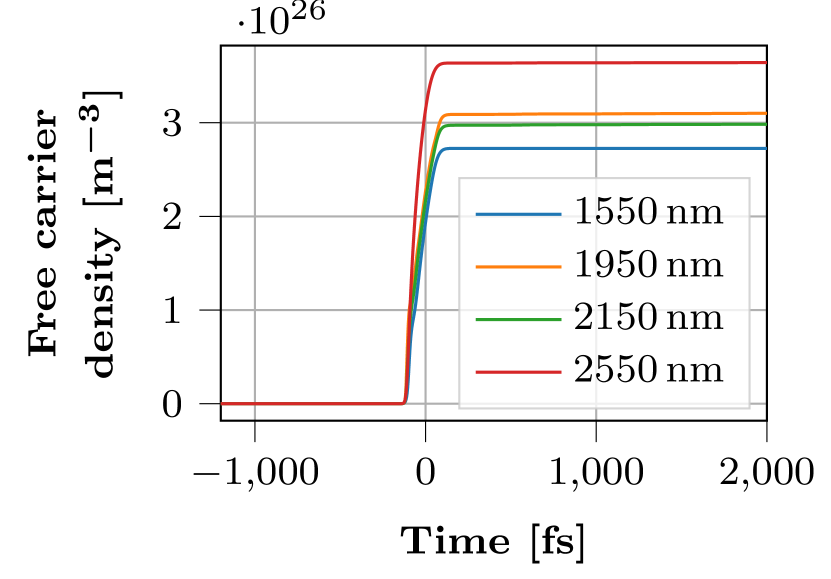
tikztikz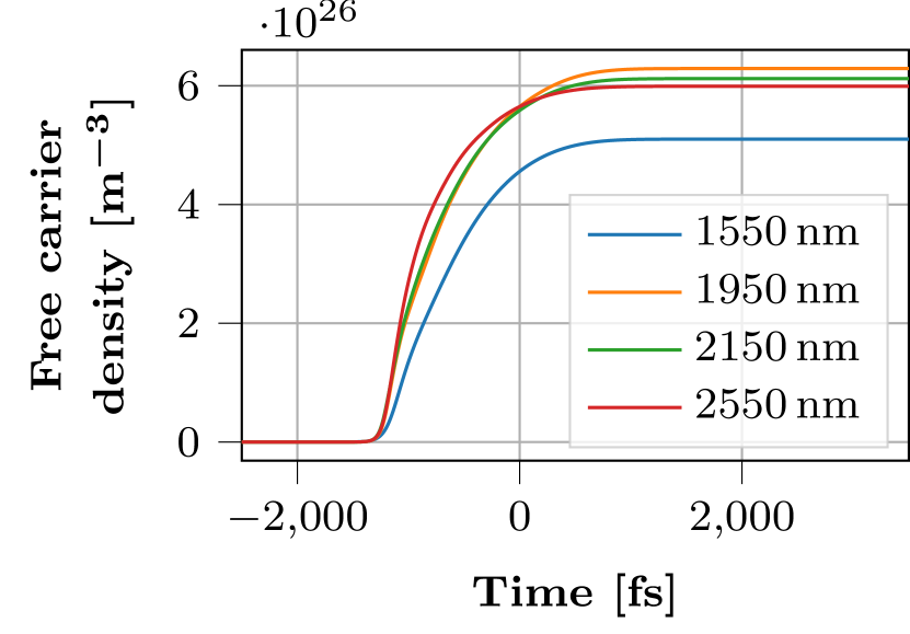
tikztikz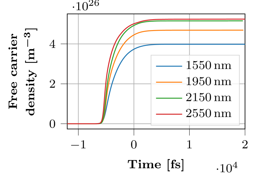
The corresponding fields (for ) are shown in Figure 13. Several effects can be seen here, and are worth mentioning:
-
•
A longer pulse looses a larger amount of energy, leading to the larger shift of the intensity peak towards the leading edge (c.f. Figures 13(a) and 13(b))
-
•
While the pulse with generates the highest intensity at the focal spot for the pulses with (c.f. Figures 17(a), 17(b) and 13(a)). For longer pulse durations () higher intensities will be generated at longer wavelengths.
-
•
Even though the pulse energy is one order of magnitude lower in Figure 13(a) than in Figure 17(a) the peak intensity value is approximately equal, indicating intensity clamping due to high absorption and diffraction.
-
•
The generated plasma density for a pulse with is larger compared to a pulse with , as shown in Figures 18(b) and 13(e), if both pulses have an energy of . This indicates a better energy deposition of the pulse energy into the material for longer pulses
-
•
While the pulse with at could generate the highest free-carrier density, this role is taken over by the pulse with for , with the pulses at and on second position.
tikztikz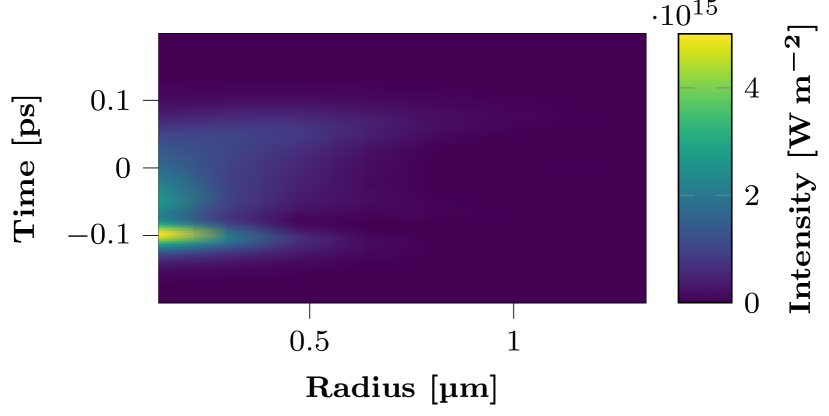
tikztikz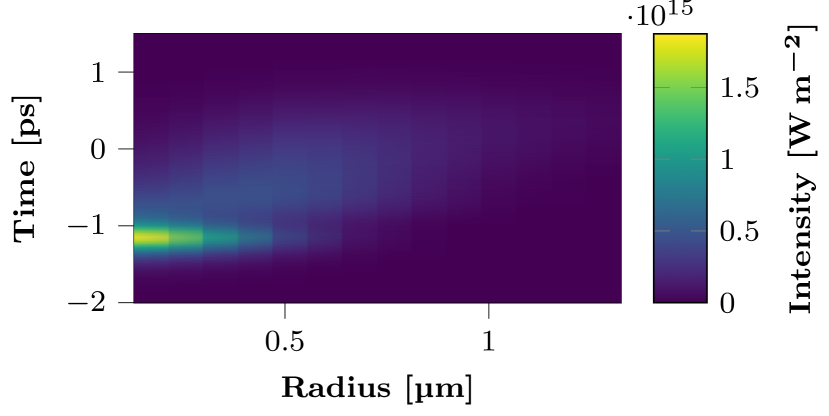
This indicates that pulses longer than are necessary to efficiently transfer energy from the pulse into the material. For a pulse duration of exemplary results are displayed in Figures 13(b) and 13(e), and for a pulse duration of those results are displayed in Figures 13(c) and 13(f). Several major differences can be noted for a pulse duration of in comparison with the data in Figure 13(b) (for ):
-
•
The pulses at and now share the peak intensity value, compared with the pulses with a shorter and longer wavelength
-
•
The peak intensity for is decreased by compared to
-
•
The peak density decreased by compared to , but is still higher by compared to a pulse duration of
As it can be seen in Figures 17, 13(c), 13(f), 13(d), 13(a), 13(b) and 13(e) the peak intensity and the carrier density vary depending on pulse duration, pulse energy and pulse wavelength if the focal depth and focusing angle is kept at a constant value. Following those graphs for a focusing depth of and a numerical aperture of /// for the different wavelengths, correspondingly, it can be seen that the maximum intensity can be achieved for short pulses with high energies. Meanwhile, the free carrier density does not follow the same pattern. Instead, very short and very long pulses generate a lower amount of free carriers compared to pulses with a duration of . The initial energy of the pulse, on the other hand, directly correlates with the generated amount of free carriers. A similar pattern can be seen for the other parameters we investigated. Regardless of focus depth or numerical aperture the maximum intensity could usually be reached for the shortest possible pulse duration, combined with the highest possible pulse energy. The maximum free carrier density, though, correlates is maximized for a medium pulse duration.
The results shown in the figures above (Figures 13(d), 13(d) and 13(f)) indicate that there is an optimum of the pulse parameters for the optimum energy deposition into the material. Even though a shorter pulse with can reach a higher intensity compared to longer pulses at the same pulse energy it is not able to transfer the energy into the material as efficiently as pulses with or , assumed the efficiency of the energy transfer is determined by the amount of excited free carriers.
tikztikz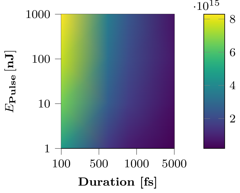
tikztikz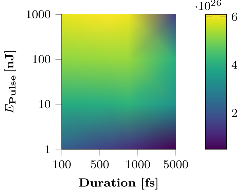
tikztikz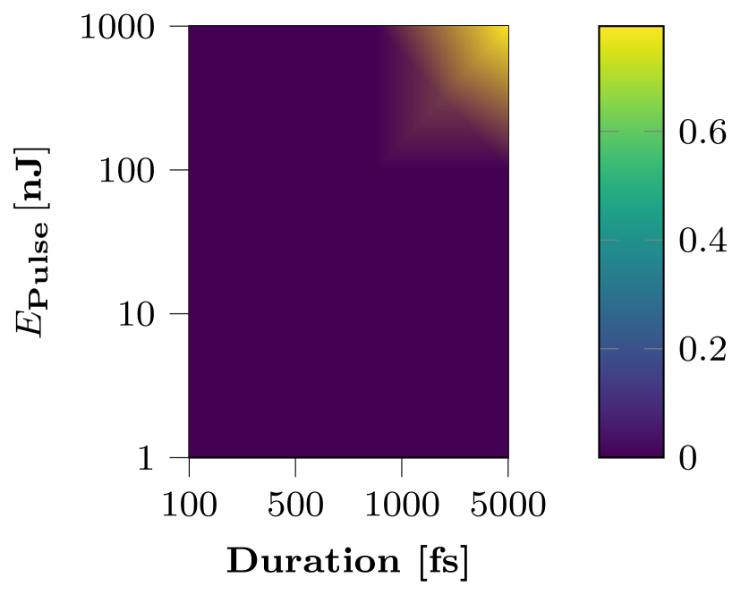
III.7 Correlation between pulse parameters and the permanent material modification
To process material it is always necessary to introduce permanent modifications in the material. As stated above in Section I.1 there are several different ways to define the lowest threshold for material modification. Following Werner et al. [51], Chambonneau et al. [7] we do not use the critical plasma density as threshold, but rather the deposited energy. This energy can be derived from the excited electrons by using Equation 1 and the assumption of full thermalization of all excited electrons. This equation together with the specific heat capacity of \ceSi (= [75]) and the latent heat of fusion of \ceSi ( [75]) gives the temperature change (and the possibility for a phase change). Using the results for the achieved free carrier density, displayed in Figures 18(a), 18(c), 18(b), 18(d) and 15(b) and ranging between , one obtains absorbed energies between . Absorbing these energies will lead to a temperature increase of . This is not sufficient for increasing the temperature of \ceSi from room temperature to the melting temperature, but sufficient to expand the heated spot slightly (with [75]). This local expansion can lead to a permanent local change of the refractive index (even without melting), which then in turn can be detected with optical methods.
This direct correlation between the generated free carrier density and the resulting change in temperature also confirms that the modification threshold does not only depend on the wavelength, but rather on the interplay between several different pulse parameters including the pulse wavelength. Especially for longer pulse durations and large focusing angles several different wavelengths can achieve approximately the same energy deposit (c.f. Figures 18(b), 18(d), 13(d), 18(a), 18(c), 13(e) and 13(f)). In that case pulse parameters other than the wavelength have a larger influence, such as initial pulse energy, pulse duration and focusing angle.
IV Conclusion and outlook
We investigated the behavior of a single pulse propagating through a material on example of \ceSi, with specific focus on achieving particularly fine processing at low pulse energies. The influence of the wavelength, the nonlinear multi-photon absorption, the third-order nonlinearity, the focusing angle, the focal depth, the pulse energy and the pulse duration were considered, with several important conclusions:
-
•
We confirmed that using wavelengths between is beneficial for maximizing the absorption of light and generation of free carriers in \ceSi even at high focusing angles compared to shorter and longer wavelengths at the optimum pulse duration. This follows from the predicted curve in the nonlinear figure of merit, which has two distinct maxima at and (as shown in Figure 2).
-
•
The importance of nonlinear effects inside \ceSi for the propagation is larger for smaller NA values. The larger the focusing angle, the less influence self-focusing and multi-photon absorption has on the propagating pulse before the focal spot. This increases the repeatability of modification generation.
-
•
The effect of nonlinear spherical aberrations or “light ring generation” was investigated. As it was shown, this effect degrades close to the maximum of the NFOM. The longer the wavelength, the better the quality of the processed structures.
-
•
The wavelength-dependent effects related to the Kerr effect and the multi-photon absorption defined by NFOM illustrate the different mechanisms of material processing. Namely, the plasma generation due to two- and three-photon absorption enhanced at by the Kerr-effect would decrease the modification threshold.
-
•
We could show that the field distribution at the focal spot only varies slightly when changing the focal depth. Increasing the focusing angle decreases changes, i.e. for larger numerical apertures the distribution of the electric field changes less when changing the target depth compared to smaller numerical apertures
-
•
It could be shown that there is an optimum pulse duration, located between , explained by the necessity to optimize the spectral overlap between the pulse and the nonlinear figure of merit.
-
•
Based on the two independent numerical approaches, we show that a nonparaxial beam structure under a plasma contribution could cause a spatio-temporal asymmetry and pulse splitting even for a comparatively small NA. Advantages of these numerical approaches are compared.
This work has thus demonstrated the importance of the careful control of laser parameters and in particular wavelength, pulse duration and energy within a large window for optimization of the energy transfer from the light pulse to the material at the focal spot. It sheds light on the different physical phenomena acting on the pulse, including the Kerr-effect, and how they can be used for optimizing the energy transfer. Further optimization and analysis can involve several directions. For example, wavelengths larger than can be investigated. As shown in Figures 2 and 3 there is a transition at from the three-photon absorption to the four-photon absorption. Placing a pulse within those two absorption regions (for example at ) would have the advantage of a decreased absorption up close to the focal spot (c.f. Figure 4), but would loose the additional benefit of increased self-focusing, as the pulses at can use.
Finally, the wavelength dependence and the impact of tunnel ionization versus multi-photon ionization and avalanche ionization can be studied and compared in a future work.
Acknowledgements
The authors would like to thank Cord Arnold (Lund University, Lund) and Andreas Erbe (NTNU, Trondheim) for the useful discussions. We also would like to thank Miroslav Kolesik (The University of Arizona, Arizona), Jeffrey Brown (Wisconsin Lutheran College, Milwaukee), Arnaud Couairon (CPHT, Ecole Polytechnique, Palaiseau) and Vladimir Fedorov (Texas A&M University at Qatar) for the very fruitful discussions about the UPPE-model. RR and ITS acknowledge financial support of the Norwegian Research Council (NFR) projects #255003 (KerfLessSi), #326503 (MIR), #303347 (UNLOCK) and ATLA Lasers AS. VK acknowledges the support from the European Union Horizon 2020 research and innovation program under the Marie Skłodowska-Curie grant No. 713694 (MULTIPLY) and the ERC Advanced Grant No. 740355 (STEMS).
Disclosures
The authors declare no conflicts of interest.
Appendix A Initial conditions for the electric field
To model the pulse as close as possible to existing experimental conditions, a Gaussian shape in time and space was chosen for the incoming pulse.
| (16) |
Here, gives the position in space perpendicular to the propagation axis, the beam radius, the wave number in vacuum, the focal length and the speed of light in vacuum. is the dispersion length, with GVD the group velocity dispersion (typically expressed in , and labelled as ). This value is defined as based on the pulse frequency and the refractive index . The pulse broadening due to dispersion is given by , and the phase shift is defined as . Finally, the phase shift introduced by the focusing lens ( in Equation 16) is defined as .
In Equation 8 we use somewhat more general initial conditions for generality. These conditions correspond to the dynamics of the Gaussian beam in the paraxial approximation:
| (17) |
| (18) | ||||
| (19) | ||||
with the parameters
| (20) |
Of course, real dynamics will differ from the Gaussian one due to nonlinear effects and non-paraxiality. Here, is the initial power (as in Equation 16), is the initial beam size, is the waist size, is the wave front curvature, is the Rayleigh length, and is the Gouy phase. The value of has a sense of intensity.
Appendix B Distribution of the temporal field and density along the propagation axis
The temporal electric field and the distribution of the generated free carriers can not only be displayed as contour plot (as shown in Figure 11), but also observed along the propagation axis. This has the advantage that slight variations in field intensity or carrier density between different focal depths or different numerical apertures are clearer, while only covering a single line along the propagation axis. Still, this also allows a direct overlap of the distribution of field or carrier density, which makes a comparison easier, and which is not possible for contour plots. The slices for the temporal field for a numerical aperture of and a focal depth of (corresponding to Figures 11(a), 11(b), 11(c) and 11(d)) are shown in Figure 16(a), and for a focal depth of at the same numerical aperture (corresponding to Figures 11(e), 11(f), 11(g) and 11(h)) are shown in Figure 16(b). For a numerical aperture of and a focal depth of (corresponding to Figures 11(i), 11(j), 11(k) and 11(l)) the temporal intensity is displayed in Figure 17(a), and for a focal depth of (without corresponding figures in Figure 11) the intensity is displayed in Figure 17(b). The density of the excited free carriers corresponding to Figures 16(a), 16(b), 17(a) and 17(b) is displayed in Figures 18(a), 18(c), 18(b) and 18(d).
tikztikz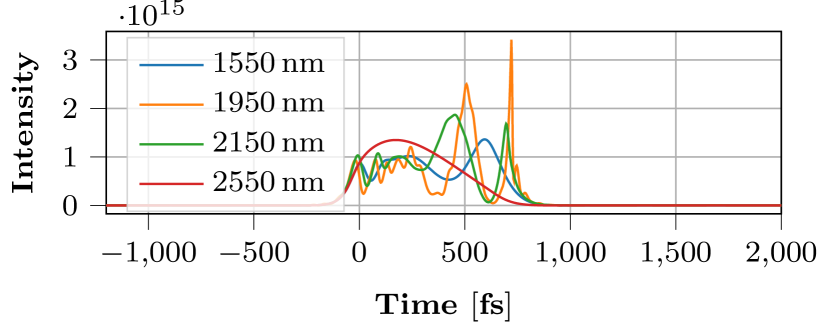
tikztikz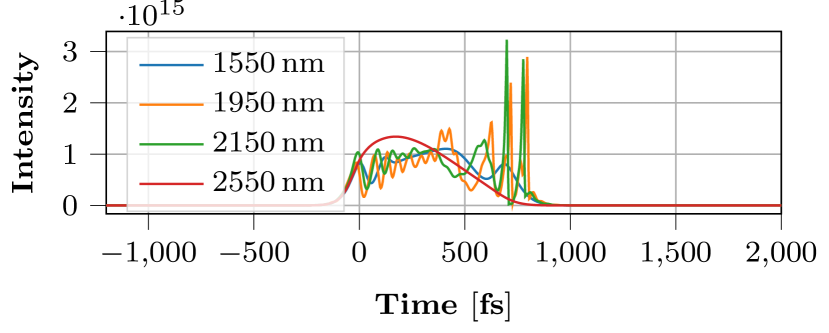
tikztikz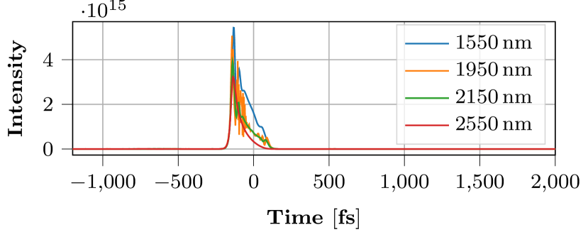
tikztikz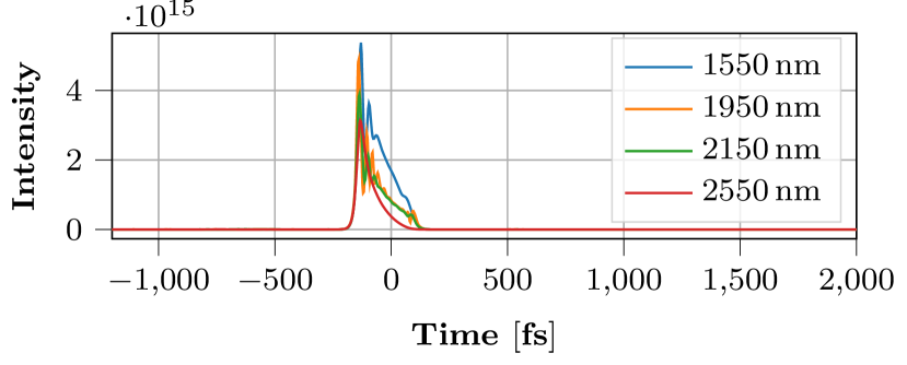
tikztikz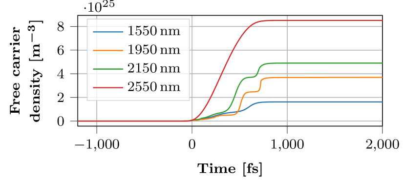
tikztikz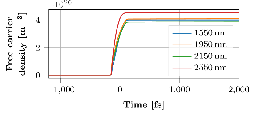
tikztikz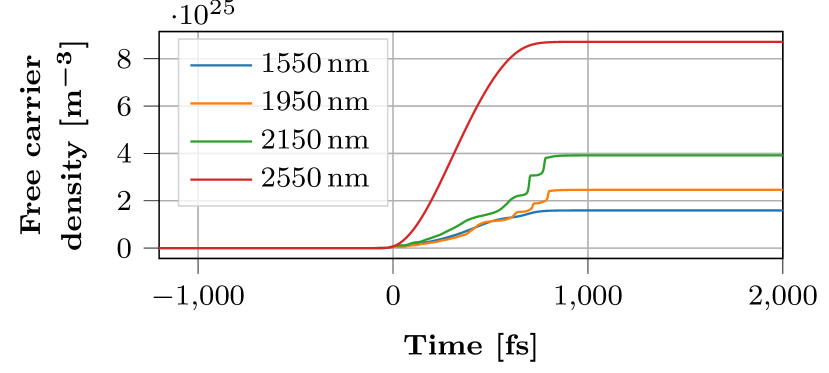
tikztikz
References
- Ohmura et al. [2006] E. Ohmura, F. Fukuyo, K. Fukumitsu, and H. Morita, Internal modified-layer formation mechanism into silicon with nanosecond laser, Journal of Achievements in Materials and Manufacturing Engineering 17, 381 (2006).
- Kumagai et al. [2006] M. Kumagai, N. Uchiyama, E. Ohmura, R. Sugiura, K. Atsumi, and K. Fukumitsu, Advanced dicing technology for semiconductor wafer -Stealth Dicing, in 2006 IEEE International Symposium on Semiconductor Manufacturing (IEEE, 2006) pp. 215–218.
- Ohmura et al. [2007] E. Ohmura, F. Fukuyo, K. Fukumitsu, and H. Morita, Modified-layer formation mechanism into silicon with permeable nanosecond laser, International Journal of Computational Materials Science and Surface Engineering 1, 677 (2007).
- Chambonneau et al. [2016] M. Chambonneau, Q. Li, M. Chanal, N. Sanner, and D. Grojo, Writing waveguides inside monolithic crystalline silicon with nanosecond laser pulses, Optics Letters 41, 4875 (2016).
- Franta et al. [2018] B. Franta, E. Mazur, and S. K. Sundaram, Ultrafast laser processing of silicon for photovoltaics, International Materials Reviews 63, 227 (2018).
- Chambonneau et al. [2018] M. Chambonneau, D. Richter, S. Nolte, and D. Grojo, Inscribing diffraction gratings in bulk silicon with nanosecond laser pulses, Optics Letters 43, 6069 (2018).
- Chambonneau et al. [2021] M. Chambonneau, D. Grojo, O. Tokel, F. Ö. Ilday, S. Tzortzakis, and S. Nolte, In‐Volume Laser Direct Writing of Silicon—Challenges and Opportunities, Laser & Photonics Reviews 15, 2100140 (2021).
- Panchal et al. [2021] N. Panchal, V. Narayanan, and D. Marla, Nanosecond Laser Processing for Improving the Surface Characteristics of Silicon Wafers Cut Using Wire Electrical Discharge Machining, Lasers in Manufacturing and Materials Processing 8, 183 (2021).
- Verburg [2015] P. C. Verburg, Laser-induced subsurface modification of silicon wafers, Ph.D. thesis, University of Twente, Enschede, The Netherlands (2015).
- Nejadmalayeri et al. [2005] A. H. Nejadmalayeri, P. R. Herman, J. Burghoff, M. Will, S. Nolte, and A. Tünnermann, Inscription of optical waveguides in crystalline silicon by mid-infrared femtosecond laser pulses, Optics Letters 30, 964 (2005).
- Zavedeev et al. [2014] E. V. Zavedeev, V. V. Kononenko, V. M. Gololobov, and V. I. Konov, Modeling the effect of fs light delocalization in Si bulk, Laser Physics Letters 11, 2011 (2014).
- Grojo et al. [2015] D. Grojo, A. Mouskeftaras, P. Delaporte, and S. Lei, Limitations to laser machining of silicon using femtosecond micro-Bessel beams in the infrared, Journal of Applied Physics 117, 10.1063/1.4918669 (2015).
- Mori et al. [2015] M. Mori, Y. Shimotsuma, T. Sei, M. Sakakura, K. Miura, and H. Udono, Tailoring thermoelectric properties of nanostructured crystal silicon fabricated by infrared femtosecond laser direct writing, Physica Status Solidi (A) Applications and Materials Science 212, 715 (2015).
- Shimotsuma et al. [2016] Y. Shimotsuma, T. Sei, M. Mori, M. Sakakura, and K. Miura, Self-organization of polarization-dependent periodic nanostructures embedded in III–V semiconductor materials, Applied Physics A: Materials Science and Processing 122, 1 (2016).
- Zavedeev et al. [2016] E. V. Zavedeev, V. V. Kononenko, and V. I. Konov, Delocalization of femtosecond laser radiation in crystalline Si in the mid-IR range, Laser Physics 26, 016101 (2016).
- Richter et al. [2018] R. A. Richter, N. Tolstik, and I. T. Sorokina, In-bulk silicon processing with ultrashort pulsed lasers: Three-photon-absorption versus two-photon-absorption, in High-Brightness Sources and Light-driven Interactions, Vol. Part F87-M (OSA, Washington, D.C., 2018) p. MW4C.2.
- Kämmer et al. [2018] H. Kämmer, G. Matthäus, S. Nolte, M. Chanal, O. Utéza, and D. Grojo, In-volume structuring of silicon using picosecond laser pulses, Applied Physics A 124, 302 (2018).
- Das et al. [2020] A. Das, A. Wang, O. Uteza, and D. Grojo, Pulse-duration dependence of laser-induced modifications inside silicon, Optics Express 28, 26623 (2020).
- Mareev et al. [2020] E. I. Mareev, K. V. Lvov, B. V. Rumiantsev, E. A. Migal, I. D. Novikov, S. Y. Stremoukhov, and F. V. Potemkin, Effect of pulse duration on the energy delivery under nonlinear propagation of tightly focused Cr:forsterite laser radiation in bulk silicon, Laser Physics Letters 17, 015402 (2020).
- Blothe et al. [2021] M. Blothe, M. Chambonneau, T. Heuermann, M. Gebhardt, J. Limpert, and S. Nolte, Laying the foundations of ultrafast stealth dicing of silicon with picosecond laser pulses at 2-m wavelength, in 2021 Conference on Lasers and Electro-Optics Europe & European Quantum Electronics Conference (CLEO/Europe-EQEC), Vol. 016101 (IEEE, 2021) pp. 1–1.
- Richter et al. [2020] R. A. Richter, N. Tolstik, S. Rigaud, P. D. Valle, A. Erbe, P. Ebbinghaus, I. Astrauskas, V. Kalashnikov, E. Sorokin, and I. T. Sorokina, Sub-surface modifications in silicon with ultra-short pulsed lasers above 2 µm, Journal of the Optical Society of America B 37, 2543 (2020), arXiv:1907.13186 .
- Tokel et al. [2017] O. Tokel, A. Turnalı, G. Makey, P. Elahi, T. Çolakoğlu, E. Ergeçen, Ö. Yavuz, R. Hübner, M. Zolfaghari Borra, I. Pavlov, A. Bek, R. Turan, D. K. Kesim, S. Tozburun, S. Ilday, and F. Ö. Ilday, In-chip microstructures and photonic devices fabricated by nonlinear laser lithography deep inside silicon, Nature Photonics 11, 639 (2017), arXiv:1409.2827 .
- Pavlov et al. [2017] I. Pavlov, O. Tokel, S. Pavlova, V. Kadan, G. Makey, A. Turnali, Ö. Yavuz, and F. Ö. Ilday, Femtosecond laser written waveguides deep inside silicon, Optics Letters 42, 3028 (2017).
- Turnali et al. [2019] A. Turnali, M. Han, and O. Tokel, Laser-written depressed-cladding waveguides deep inside bulk silicon, Journal of the Optical Society of America B 36, 966 (2019).
- Wang et al. [2020a] A. Wang, A. Das, and D. Grojo, Ultrafast Laser Writing Deep inside Silicon with THz-Repetition-Rate Trains of Pulses, Research 2020, 1 (2020a).
- Tolstik et al. [2022] N. Tolstik, E. Sorokin, J. C. I. Mac-Cragh, R. A. Richter, and I. T. Sorokina, Single-pulse laser induced buried defects in silicon written by ultrashort-pulse laser at 2.1 micro-meter, in Conference on Lasers and Electro-Optics (OSA, 2022).
- Lin et al. [2007] Q. Lin, J. Zhang, G. Piredda, R. W. Boyd, P. M. Fauchet, and G. P. Agrawal, Dispersion of silicon nonlinearities in the near infrared region, Applied Physics Letters 91, 2 (2007).
- Wang et al. [2013] T. Wang, N. Venkatram, J. Gosciniak, Y. Cui, G. Qian, W. Ji, and D. T. H. Tan, Multi-photon absorption and third-order nonlinearity in silicon at mid-infrared wavelengths, Optics Express 21, 32192 (2013).
- Kononenko et al. [2016] V. V. Kononenko, E. V. Zavedeev, and V. M. Gololobov, The effect of light-induced plasma on propagation of intense fs laser radiation in c-Si, Applied Physics A 122, 293 (2016).
- Chambonneau et al. [2020] M. Chambonneau, M. Blothe, V. Y. Fedorov, T. Heuermann, G. Matthäus, A. Alberucci, J. Limpert, S. Tzortzakis, and S. Nolte, Processing bulk silicon with femtosecond laser pulses at wavelength (Conference Presentation), in Frontiers in Ultrafast Optics: Biomedical, Scientific, and Industrial Applications XX, Vol. 11270, edited by P. R. Herman, M. Meunier, and R. Osellame, International Society for Optics and Photonics (SPIE, 2020) p. 12.
- Sorokina and Sorokin [2015] I. T. Sorokina and E. Sorokin, Femtosecond Cr 2+ -Based Lasers, IEEE Journal of Selected Topics in Quantum Electronics 21, 273 (2015).
- Slobodchikov et al. [2016] E. Slobodchikov, L. R. Chieffo, and K. F. Wall, High peak power ultrafast Cr:ZnSe oscillator and power amplifier, in Solid State Lasers XXV: Technology and Devices, Vol. 9726, edited by W. A. Clarkson and R. K. Shori (2016) p. 972603.
- Ren et al. [2018] X. Ren, L. H. Mach, Y. Yin, Y. Wang, and Z. Chang, Generation of 1 kHz, 2.3 mJ, 88 fs, 2.5 m pulses from a Cr 2+ :ZnSe chirped pulse amplifier, Optics Letters 43, 3381 (2018).
- Vasilyev et al. [2019] S. Vasilyev, J. Peppers, I. Moskalev, V. Smolski, M. Mirov, E. Slobodchikov, A. Dergachev, S. Mirov, and V. Gapontsev, 1.5-mJ Cr:ZnSe Chirped Pulse Amplifier Seeded by a Kerr-Lens Mode-Locked Cr:ZnS oscillator, in Laser Congress 2019 (ASSL, LAC, LS&C) (OSA, Washington, D.C., 2019) p. ATu4A.4.
- Duval et al. [2015] S. Duval, M. Bernier, V. Fortin, J. Genest, M. Piché, and R. Vallée, Femtosecond fiber lasers reach the mid-infrared, Optica 2, 623 (2015).
- Gu et al. [2020] H. Gu, Z. Qin, G. Xie, T. Hai, P. Yuan, J. Ma, and L. Qian, Generation of 131 fs mode-locked pulses from 2.8 m Er:ZBLAN fiber laser, Chinese Optics Letters 18, 031402 (2020).
- Wang et al. [2020b] Z. Wang, B. Zhang, J. Liu, Y. Song, and H. Zhang, Recent developments in mid-infrared fiber lasers: Status and challenges, Optics and Laser Technology 132, 106497 (2020b).
- Biswas and Ambegaokar [1982] R. Biswas and V. Ambegaokar, Phonon spectrum of a model of electronically excited silicon, Physical Review B 26, 1980 (1982).
- Stampfli and Bennemann [1990] P. Stampfli and K. H. Bennemann, Theory for the laser-induced instability of the diamond structure of Si, Ge and C, Progress in Surface Science 35, 161 (1990).
- Stampfli and Bennemann [1992] P. Stampfli and K. H. Bennemann, Dynamical theory of the laser-induced lattice instability of silicon, Physical Review B 46, 10686 (1992).
- Sokolowski-Tinten et al. [1995] K. Sokolowski-Tinten, J. Bialkowski, and D. Von Der Linde, Ultrafast laser-induced order-disorder transitions in semiconductors, Physical Review B 51, 14186 (1995).
- Sokolowski-Tinten and von der Linde [2000] K. Sokolowski-Tinten and D. von der Linde, Generation of dense electron-hole plasmas in silicon, Physical Review B 61, 2643 (2000).
- Apostolova et al. [2020] T. Apostolova, B. Obreshkov, and I. Gnilitskyi, Ultrafast energy absorption and photoexcitation of bulk plasmon in crystalline silicon subjected to intense near-infrared ultrashort laser pulses, Applied Surface Science 519, 146087 (2020), arXiv:1910.09023 .
- Apostolova and Obreshkov [2022] T. Apostolova and B. Obreshkov, Femtosecond optical breakdown in silicon, Applied Surface Science 572, 151354 (2022), arXiv:2107.07189 .
- Du et al. [1994] D. Du, X. Liu, G. Korn, J. Squier, and G. Mourou, Laser-induced breakdown by impact ionization in SiO2 with pulse widths from 7 ns to 150 fs, Applied Physics Letters 64, 3071 (1994).
- B.C et al. [1995] S. B.C, F. M. D, R. A. M, S. B.W, and P. M. D, Laser-Induced Damage in Dielectrics with Nanosecond to Subpicosecond Pulses, Physical Review Letters 74, 2248 (1995).
- Du et al. [1996] D. Du, X. Liu, and G. Mourou, Reduction of multi-photon ionization in dielectrics due to collisions, Applied Physics B: Lasers and Optics 63, 617 (1996).
- Tien et al. [1999] A. C. Tien, S. Backus, H. Kapteyn, M. Murnane, and G. Mourou, Short-pulse laser damage in transparent materials as a function of pulse duration, Physical Review Letters 82, 3883 (1999).
- Chimier et al. [2011] B. Chimier, O. Utéza, N. Sanner, M. Sentis, T. Itina, P. Lassonde, F. Légaré, F. Vidal, and J. C. Kieffer, Damage and ablation thresholds of fused-silica in femtosecond regime, Physical Review B 84, 094104 (2011).
- Zhokhov and Zheltikov [2018] P. A. Zhokhov and A. M. Zheltikov, Optical breakdown of solids by few-cycle laser pulses, Scientific Reports 8, 1824 (2018).
- Werner et al. [2019] K. Werner, V. Gruzdev, N. Talisa, K. R. P. Kafka, D. Austin, C. M. Liebig, and E. A. Chowdhury, Single-Shot Multi-Stage Damage and Ablation of Silicon by Femtosecond Mid-infrared Laser Pulses, Scientific Reports 9, 1 (2019).
- Gamaly et al. [2002] E. G. Gamaly, A. V. Rode, B. Luther-Davies, and V. T. Tikhonchuk, Ablation of solids by femtosecond lasers: Ablation mechanism and ablation thresholds for metals and dielectrics, Physics of Plasmas 9, 949 (2002).
- Fedorov et al. [2016] V. Y. Fedorov, M. Chanal, D. Grojo, and S. Tzortzakis, Accessing Extreme Spatiotemporal Localization of High-Power Laser Radiation through Transformation Optics and Scalar Wave Equations, Physical Review Letters 117, 043902 (2016).
- Kolesik et al. [2002] M. Kolesik, J. V. Moloney, and M. Mlejnek, Unidirectional Optical Pulse Propagation Equation, Physical Review Letters 89, 283902 (2002).
- Fibich [1996] G. Fibich, Small beam nonparaxiality arrests self-focusing of optical beams, Phys. Rev. Lett. 76, 4356 (1996).
- Krupa et al. [2017] K. Krupa, A. Tonello, B. M. Shalaby, M. Fabert, A. Barthélémy, G. Millot, S. Wabnitz, and V. Couderc, Spatial beam self-cleaning in multimode fibres, Nature Photonics 11, 237 (2017), arXiv:1603.02972 .
- Krupa et al. [2019] K. Krupa, A. Tonello, A. Barthélémy, T. Mansuryan, V. Couderc, G. Millot, P. Grelu, D. Modotto, S. A. Babin, and S. Wabnitz, Multimode nonlinear fiber optics, a spatiotemporal avenue, APL Photonics 4, 110901 (2019).
- Bristow et al. [2007] A. D. Bristow, N. Rotenberg, and H. M. van Driel, Two-photon absorption and Kerr coefficients of silicon for 850–2200nm, Applied Physics Letters 90, 191104 (2007).
- Pearl et al. [2008] S. Pearl, N. Rotenberg, and H. M. van Driel, Three photon absorption in silicon for 2300 – 3300 nm, Applied Physics Letters 93, 131102 (2008).
- Gai et al. [2013] X. Gai, Y. Yu, B. Kuyken, P. Ma, S. J. Madden, J. Van Campenhout, P. Verheyen, G. Roelkens, R. Baets, and B. Luther-Davies, Nonlinear absorption and refraction in crystalline silicon in the mid-infrared, Laser & Photonics Reviews 7, 1054 (2013).
- Li [1980] H. H. Li, Refractive index of silicon and germanium and its wavelength and temperature derivatives, Journal of Physical and Chemical Reference Data 9, 561 (1980).
- Mizrahi et al. [1989] V. Mizrahi, M. A. Saifi, M. J. Andrejco, K. W. DeLong, and G. I. Stegeman, Two-photon absorption as a limitation to all-optical switching, Optics Letters 14, 1140 (1989).
- Gholami et al. [2011] F. Gholami, S. Zlatanovic, A. Simic, L. Liu, D. Borlaug, N. Alic, M. P. Nezhad, Y. Fainman, and S. Radic, Third-order nonlinearity in silicon beyond 2350 nm, Applied Physics Letters 99, 1 (2011).
- Couairon et al. [2011] A. Couairon, E. Brambilla, T. Corti, D. Majus, O. de J. Ramírez-Góngora, and M. Kolesik, Practitioner’s guide to laser pulse propagation models and simulation, The European Physical Journal Special Topics 199, 5 (2011), arXiv:arXiv:1011.1669v3 .
- Couairon et al. [2015] A. Couairon, O. G. Kosareva, N. A. Panov, D. E. Shipilo, V. A. Andreeva, V. Jukna, and F. Nesa, Propagation equation for tight-focusing by a parabolic mirror, Optics Express 23, 31240 (2015).
- Chang et al. [1999] Q. Chang, E. Jia, and W. Sun, Difference schemes for solving the generalized nonlinear schrödinger equation, Journal of Computational Physics 148, 397 (1999).
- Bertolani et al. [2003] A. Bertolani, A. Cucinotta, S. Selleri, l. Vincetti, and M. Zoboli, Overview on finite-element time-domain approaches for optical propagation analysis, Optical and Quantum Electronics 35, 1005 (2003).
- Kononenko et al. [2012] V. V. Kononenko, V. V. Konov, and E. M. Dianov, Delocalization of femtosecond radiation in silicon, Optics Letters 37, 3369 (2012).
- Arndt et al. [tion] D. Arndt, W. Bangerth, B. Blais, M. Fehling, R. Gassmöller, T. Heister, L. Heltai, U. Köcher, M. Kronbichler, M. Maier, P. Munch, J.-P. Pelteret, S. Proell, K. Simon, B. Turcksin, D. Wells, and J. Zhang, The deal.II library, version 9.3, Journal of Numerical Mathematics 29, 171 (2021, accepted for publication).
- Arndt et al. [2021] D. Arndt, W. Bangerth, D. Davydov, T. Heister, L. Heltai, M. Kronbichler, M. Maier, J.-P. Pelteret, B. Turcksin, and D. Wells, The deal.II finite element library: Design, features, and insights, Computers & Mathematics with Applications 81, 407 (2021).
- Balay et al. [1997] S. Balay, W. D. Gropp, L. C. McInnes, and B. F. Smith, Efficient management of parallelism in object oriented numerical software libraries, in Modern Software Tools in Scientific Computing, edited by E. Arge, A. M. Bruaset, and H. P. Langtangen (Birkhäuser Press, 1997) pp. 163–202.
- Balay et al. [2019] S. Balay, S. Abhyankar, M. F. Adams, J. Brown, P. Brune, K. Buschelman, L. Dalcin, V. Eijkhout, W. D. Gropp, D. Karpeyev, D. Kaushik, M. G. Knepley, D. A. May, L. C. McInnes, R. T. Mills, T. Munson, K. Rupp, P. Sanan, B. F. Smith, S. Zampini, H. Zhang, and H. Zhang, PETSc Users Manual, Tech. Rep. ANL-95/11 - Revision 3.11 (2019).
- Själander et al. [2019] M. Själander, M. Jahre, G. Tufte, and N. Reissmann, EPIC: An energy-efficient, high-performance GPGPU computing research infrastructure (2019), arXiv:1912.05848 [cs.DC] .
- Richter et al. [2021] R. A. Richter, V. L. Kalashnikov, and I. T. Sorokina, Wavelength-dependent modification of silicon by femtosecond pulses, in Conference on Lasers and Electro-Optics (2021) p. JTh3A.73.
- Chase [1998] M. W. J. Chase, NIST-JANAF thermochemical tables, fourth edi ed., edited by A. C. Society (American Institute of Physics for the National Institute of Standards and Technology, Washington, D.C., 1998).