Two-dimensional MoSi2N4: An Excellent 2D Semiconductor for Field-Effect Transistors
Abstract
We report the performance of field-effect transistors (FETs), comprised of mono-layer of recently synthesized layered two-dimensional MoSi2N4 as channel material, using the first principles quantum transport simulations. The devices’ performance is assessed as per the International Roadmap for Devices and Systems (IRDS) 2020 roadmap for the year 2034 and compared to advanced silicon-based FETs, carbon nanotube-based FETs, and other promising two-dimensional materials based FETs. Finally, we estimate the figure of merits of a combinational and a sequential logic circuit based on our double gate devices and benchmark against promising alternative logic technologies. The performance of our devices and circuits based on them are encouraging, and competitive to other logic alternatives.
Index Terms:
Field-effect transistors (FETs), Density functional Theory (DFT), Maximally-localised Wannier functions (MLWF), Non-equilibrium Greens function (NEGF), Quantum Transport (QT), Mono-layer (ML).I Introduction
The two-dimensional (2D) semiconductors are promising channel materials for future technology nodes, owing to the ultrathin thickness (), no surface dangling bonds, and sharp turn-on of the density of states (DOS) at band edges[1, 2, 3, 4]. In the last five years, there has been remarkable progress on synthesizing novel 2D semiconductors and several promising device concepts[5, 6, 7] have been demonstrated based on them. Also, the shortest MoS2 transistor with -gate length has been fabricated, which shows a near-ideal sub-threshold swing of and an ON/OFF current ratio of [8].
The 2D semiconductors materials library has been enriched due to their bulk, arranged in layered form, in which intra-layers bonds are strong covalent bonds and weak Van der Walls (vdW) force connects inter-layers. Advanced experimental techniques have been used to isolate their layers from bulk. But, most bulk materials are non-layered (strong covalent bonds connect all three dimensions). Thus, the exfoliation process can not create their 2D structure. Recently, Silicon has been introduced as a passivator during the CVD growth of non-layered molybdenum nitride ()[9]. This process results in the growth of the centimeter-scale film of layered 2D MoSi2N4.
Mono-layer (ML) MoSi2N4 has excellent mechanical, electronic, optical, and thermal properties[9, 10, 11, 12, 13]. It is also a promising photocatalyst for water splitting and reduction[10, 12]. It has been shown that ML-MoSi2N4 has excellent stability (far better than other 2D semiconductors), using phonon, molecular dynamics (MD) calculations, and experimental testing. Even it can be handled, processed, and stored without any protective environment, unlike black phosphorus (In ambient conditions, black phosphorus (BP) can be easily etched due to chemical degradation[14]) and MoS2 (In moist air below , its surface starts oxidizing[15]). The Young’s modulus and breaking strength for ML-MoSi2N4 are and , respectively. These values are more than double of ML-MoS2. ML-MoSi2N4 is an indirect band gap semiconductor with the experimental band gap value of . Its elastic constant is times of ML-MoS2, and the carrier mobilities in it are times and - times of ML-MoS2 (the most widely studied 2D material for FETs application[16, 17, 8, 18, 19, 20, 21, 22, 23, 24, 25, 26, 27, 28]). Its lattice thermal conductivities[12, 11] are approximately 1.6 times silicon (Si) and much higher than other widely known 2D semiconductors[29, 30, 31] (ML-MoS2, As, Sb, silicene and, ML-BP), but much lower than graphene[32, 29]. The high lattice thermal conductivity of ML-MoSi2N4 ensures a high rate of heat removal through nano-electronic devices comprised of this material. Its optical transmittance is high () and comparable to graphene. The metal contacts to the ML of MoSi2N4 show exceptional physical properties with a large Schottky barrier height slope parameter, outperforming most other 2D semiconductors. CMOS compatible metals (Sc and Ti) also show excellent ohmic contact to ML-MoSi2N4 with zero interfacial tunneling barrier[33, 34]. Overall, Mono-layer MoSi2N4 is an excellent semiconductor for logic applications. However, there is a need to investigate the transport properties of FETs based on ML-MoSi2N4, and performance of integrated circuits (ICs) comprised of MoSi2N4 FETs.
Here, we exploit the capabilities of maximally localized Wannier functions (MLWFs) [35, 36, 37] to model electronic structure of ML-MoSi2N4 and generate tight-binding (TB) like Hamiltonian for the targeted device dimensions. Next, we compute transport properties of n- and p-type devices based on this ML by solving coupled Poisson and Schrdinger equations in non-equilibrium Green’s functions (NEGF) formalism. We assess the performance of MoSi2N4 based FETs as per the requirements of International Roadmap for Devices and Systems (IRDS) 2020 for the year 2034[38]. The channel length scalability of devices is also studied with their switching performance. Finally, the figure of merits (FOMs) of a combinational circuit (32-bit adder) and a sequential circuit (ALU) are estimated and benchmarked against promising logic technologies (CMOS and beyond-CMOS).
II Computational Methods
Vienna Ab initio Simulation Package (VASP)[39], a tool based on DFT, is used to relax the atomic positions and calculate the electronic structure of ML-MoSi2N4. The Projector Augmented Wave (PAW)[40] pseudopotentials with plane-wave basis set are used for DFT calculations. The generalized gradient approximation (GGA) developed by Perdew-Burke-Ernzerhof (PBE)[41] is used to consider exchange and correlation effects. The energy cutoff of 400 eV is used for the plane-wave basis set, and the Brillouin zone integrations are performed using k-mesh.
The obtained Bloch/plane-wave states from DFT calculations are mapped to MLWFs using the Wannier90 suite of codes[42]. The obtained TB-like Hamiltonian in MLWF basis is used to construct the Hamiltonian for targeted device dimensions. In the transverse direction (channel width direction), periodic boundary condition (PBC) is considered with 30 uniform wave-vector samples. The constructed device Hamiltonian is used as input to solve coupled Schrdinger and Poisson equations in Non-equilibrium Green’s functions (NEGF) formalism[43, 44, 45, 46]. Additional computational details are described in Appendix.
III Results
III-A Structural and Electrical Properties of ML-MoSi2N4
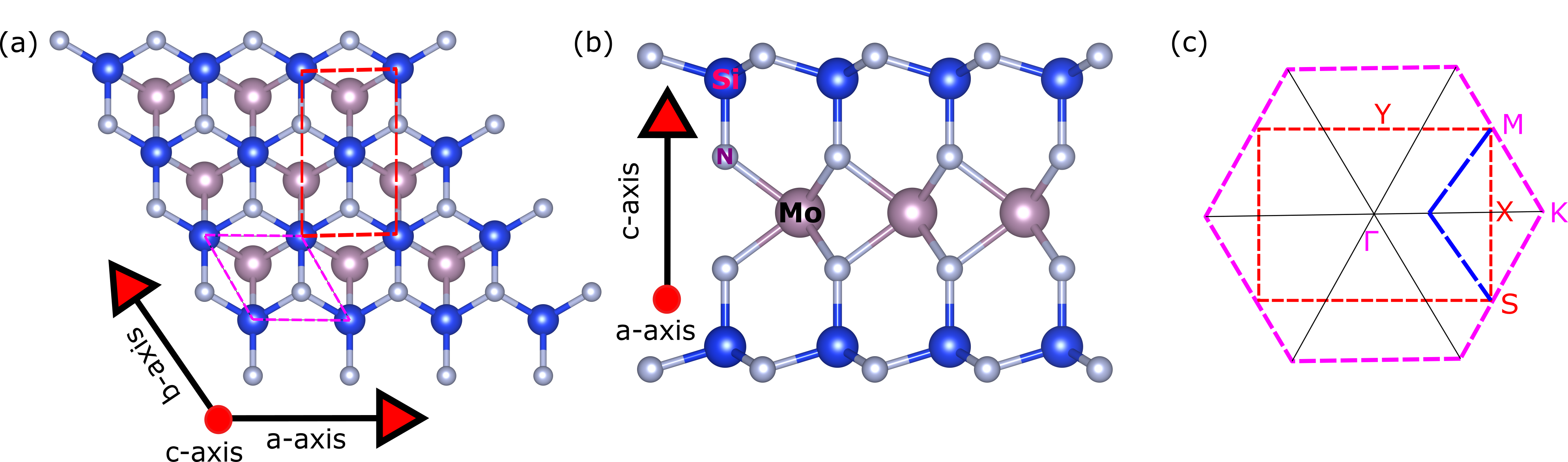
The two dimensional periodic replication of one Mo, two Si, and four N atoms, packed in honey-comb lattice, generate the ML of MoSi2N4 (see Fig. 1 (a) and (b)). This ML can be viewed as ( like structure) sandwitched between two buckled honeycomb SiN layers (see Fig. 1 (b)). The optimized lattic constant is 2.90 Å and the thickness of ML is 7.01 Å. The optimized structural parameters agree well with the literature[47, 48, 10].
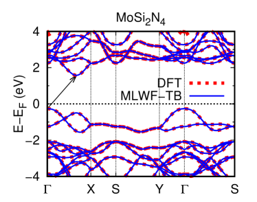
The electronic band structure of MoSi2N4 is plotted along with the high symmetry points (-----) in the orthogonal Brillouin zone (BZ). Figure. 1 (c) shows the BZ associated with hexagonal cell and orthogonal cell. Figure. 2 shows the band structure of MoSi2N4 obtained from DFT and MLWF-TB Hamiltonian. The band structure from MLWF-TB Hamiltonian shows a good match with DFT near VBM and CBM. It is an indirect band gap semiconductor with the conduction band maxima (CBM) lies in the way from to (equivalent to in hexagonal BZ) and valance band maxima (VBM) at . The curvature of CBM and VBM are isotropic, but the curvature of CBM is larger than the curvature of VBM. Hence, larger effective mass for holes () than electrons () i.e., (see Table I).
III-B Device Structure and Electrical Characteristics
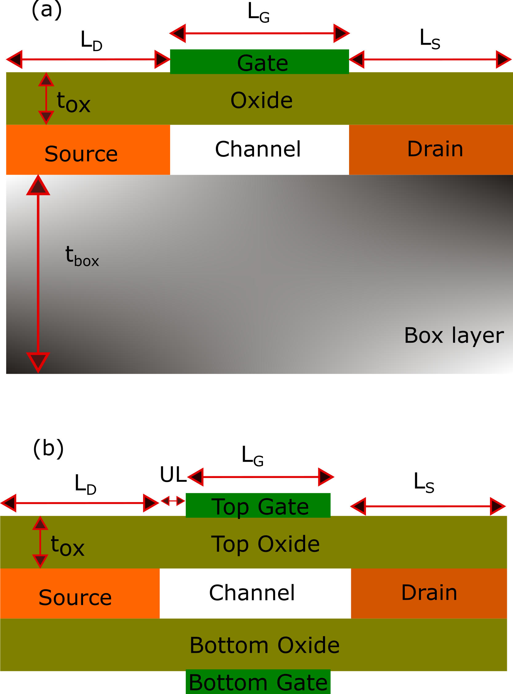
The Single gate (SG) and double-gate (DG) devices, using ML of MoSi2N4 as channel material, are investigated. Figure. 3 (a) and 3 (b) show the schematic of SG and DG devices, respectively. The geometrical parameters of the devices are gate length (), channel length (), source/drain extension , underlap length (UL), and oxide thickness (). For SG, is BOX layer thickness with = . Silicon dioxide (SiO2) is used as gate oxide and BOX layer. This work aims to assess the intrinsic performance of FETs based on the mono-layer of MoSi2N4. Hence, the S/channel/D doping used in the device simulations are n+/undoped (intrinsic)/n+ and p+/undoped (intrinsic)/p+ for n- and p-type devices, respectively. The S/D is doped such that the Fermi level is above/below the conduction/valance band for n-FET/p-FET. The metal gate work function is tuned to get (say it OFF-current () at for all the simulated devices.
We start the investigation by simulating SG and DG devices with , equivalent oxide thickness (EOT) = , and . The source-to-drain tunneling is negligible for the devices with , and the band-to-band tunneling is negligible due to the high value of band gap in this ML. These device parameters are considered according to IRDS 2020 roadmap for the year 2034. According to the roadmap, the expected channel materials are germanium (Ge) and 2D materials, and the expected devices are 2D materials based devices and FeFETs for the year 2034[38]. Figure. 4 shows the transfer characteristics for n-FETs and p-FETs. In both types, DG configuration shows a steeper sub-threshold slope (SS) and higher than SG.
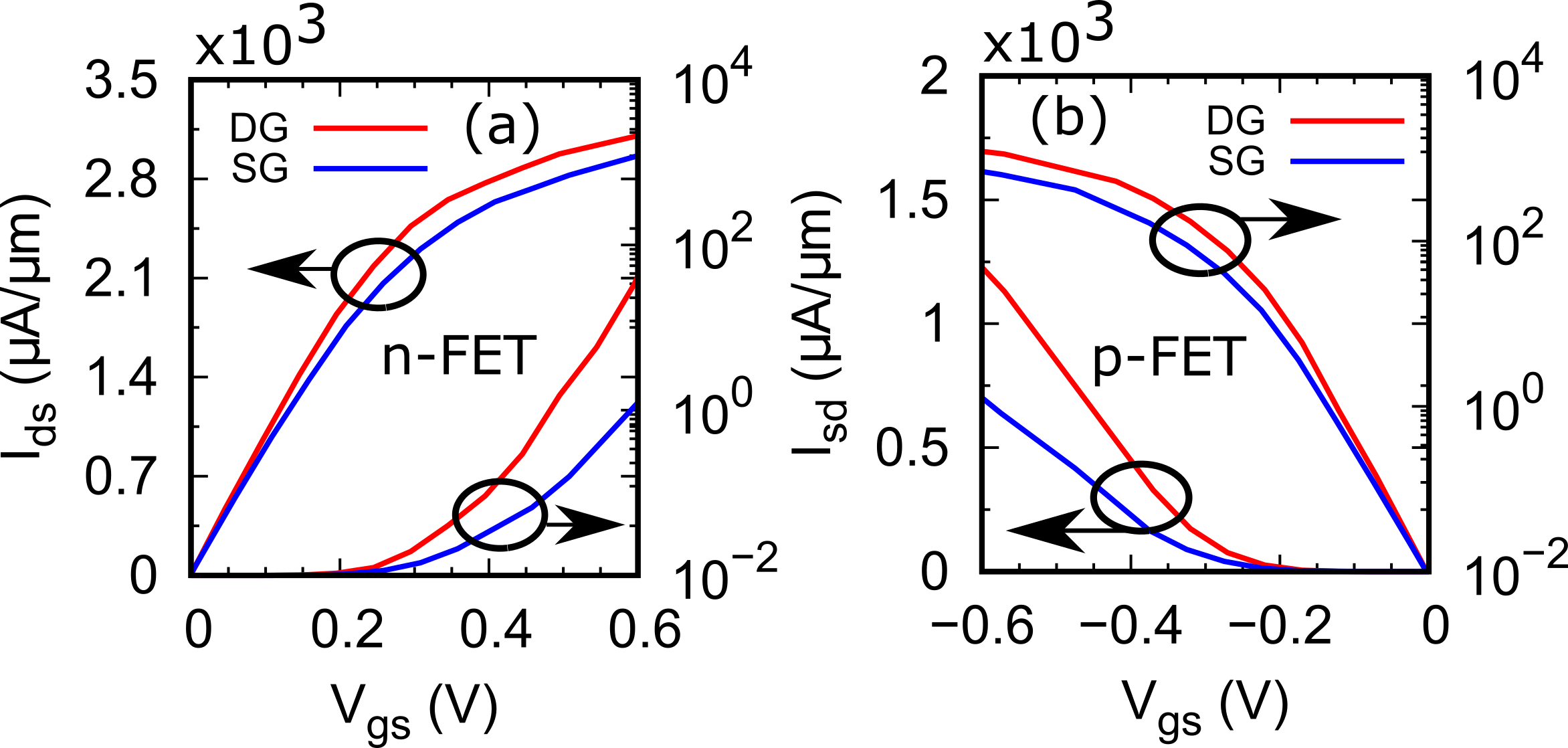
The SS for thermionic current is proportional to [49], where is quantum capacitance and is oxide capacitance. For DG configuration, oxide capacitance is double than SG, hence DG devices show better SS than SG for . The stepper SS and higher value of in DG ensure higher and higher mobile carrier concentration, respectively than SG, hence higher than SG. Defects and series parasitics resistance from contacts and S/D access region are not included in our simulations, usually limiting the device’s performance.
III-B1 Channel length Scaling
The channel length scaling is performed to study the scalability and immunity to source-to-drain tunneling (SDT) of ML-MoSi2N4 based FETs. The SDT plays a significant role in deteriorating device performance at short channel lengths. It is more severe for the low effective mass carriers than high effective mass, as the tunneling probability[50] is proportional to . Figures. 5 (a), (b), (c), and (d) show the transfer characteristics of DG n-FET, DG p-FET, SG n-FET, and SG p-FET, respectively for various channel lengths = 12, 8, 5, 3 nm.
| \rowcolorlightgray | (Å) | (Å) | VBM/CBM | |||
|---|---|---|---|---|---|---|
| MoSi2N4 | 2.90 | 7.01 | 1.842 | 0.478 | 1.184 | / -X |
The impact of SDT is more for n-type devices than p-type because the curvature of CBM is greater than VBM. For each type, DG is more immune to SDT than SG as DG shows better gate controllability than SG. Hence, DG devices are more scalable than SG. The best scalable device is DG p-FET, and it can be scaled down to 5 nm. At = , DG p-FET show SS 65 and for LP applications; For HP applications, it shows SS 67 mV/decade and .
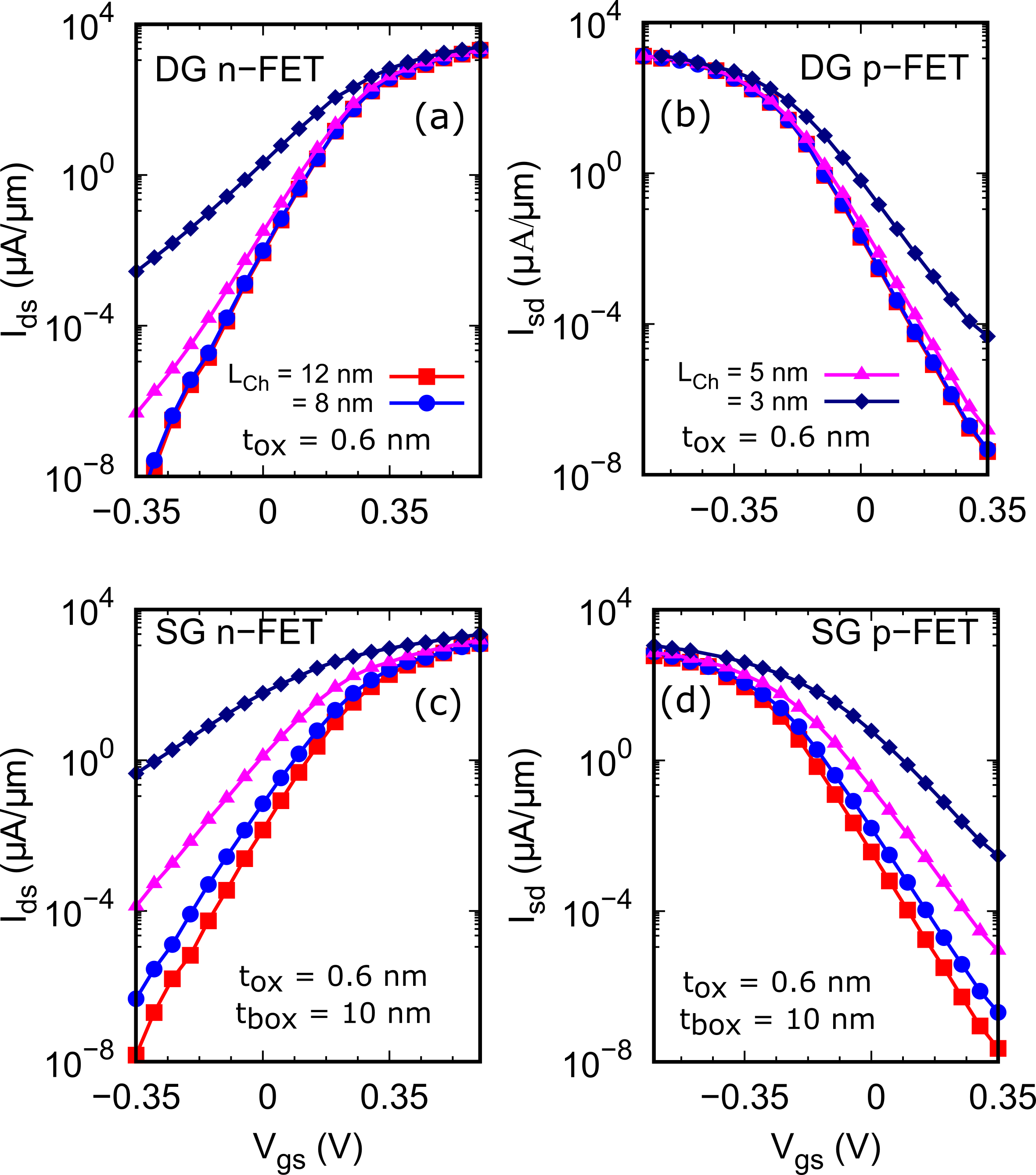
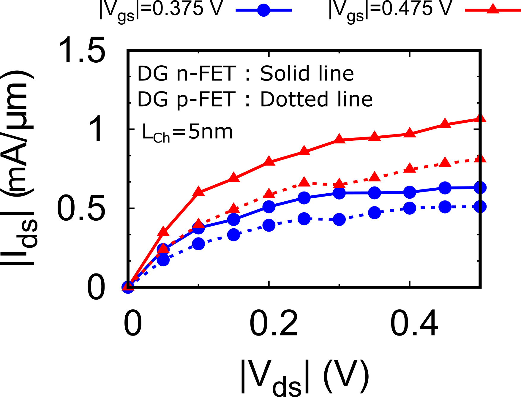
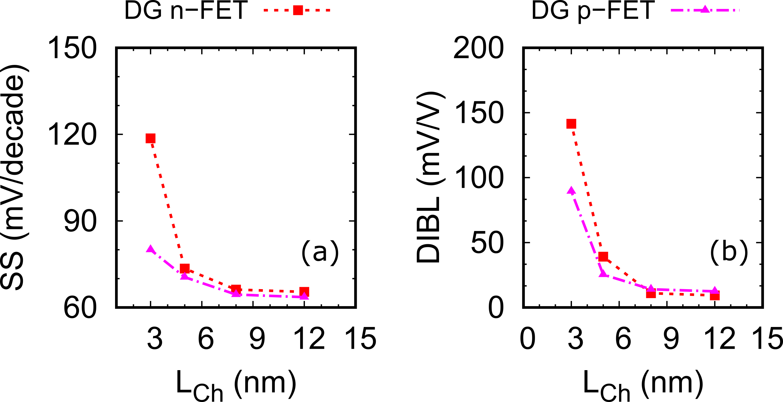
Figure. 6 shows the output characteristics of DG n-FET and p-FET with = 5 nm. Figure. 7 shows and SS of n-FET and p-FET for various at three different values of . Also, for a full assessment of DG devices at short channel lengths, DIBL is estimated from the change in threshold voltage () obtained by varying from (= 50 mV) to . Figures. 8 (a) and (b) show the variations of SS and DIBL with , respectively. Figure. 9 shows the variation of vs. for DG n- and p-FETs based on ML-MoSi2N4 and other promising 2D materials.
For both types, the ML-BP FETs show the highest [51, 52] among others (the data is not shown in the figure). But, the stability of BP remains the primary concern[14]. For n-type devices: (1) For , ML-As, and ML-Bi2O2Se have high than ML-MoSi2N4. However, the preparation of As can produce toxic arsenic trioxide, making its fabrication more complex, other than stability issue[53]. ML-Bi2O2Se shows good environmental stability[54]. But the short-channel effects are more in ML-As and ML-Bi2O2Se than ML-MoSi2N4. (2) ML-InSe shows the lower value of than ML-MoSi2N4 and the difference increases as we go below channel length. However, compelling surface oxidation in InSe deteriorates mobility and causes uncontrollable current hysteresis in InSe FETs[55]. (3) The ML-MoSi2N4 shows superior ON-state current than ML-MoS2 FETs. For p-type devices: (1) Except InSe, the MoSi2N4 shows superior ON-state current than others for . (2) The for ML-MoSi2N4 is very close to ML-Bi2O2Se and superior to others for . BL-Bi2O2Se suffers from high leakage current due to small bandgap ( ), and is much lower than ML-MoSi2N4 for both n- and p-type devices.


III-B2 Switching Performance of FETs
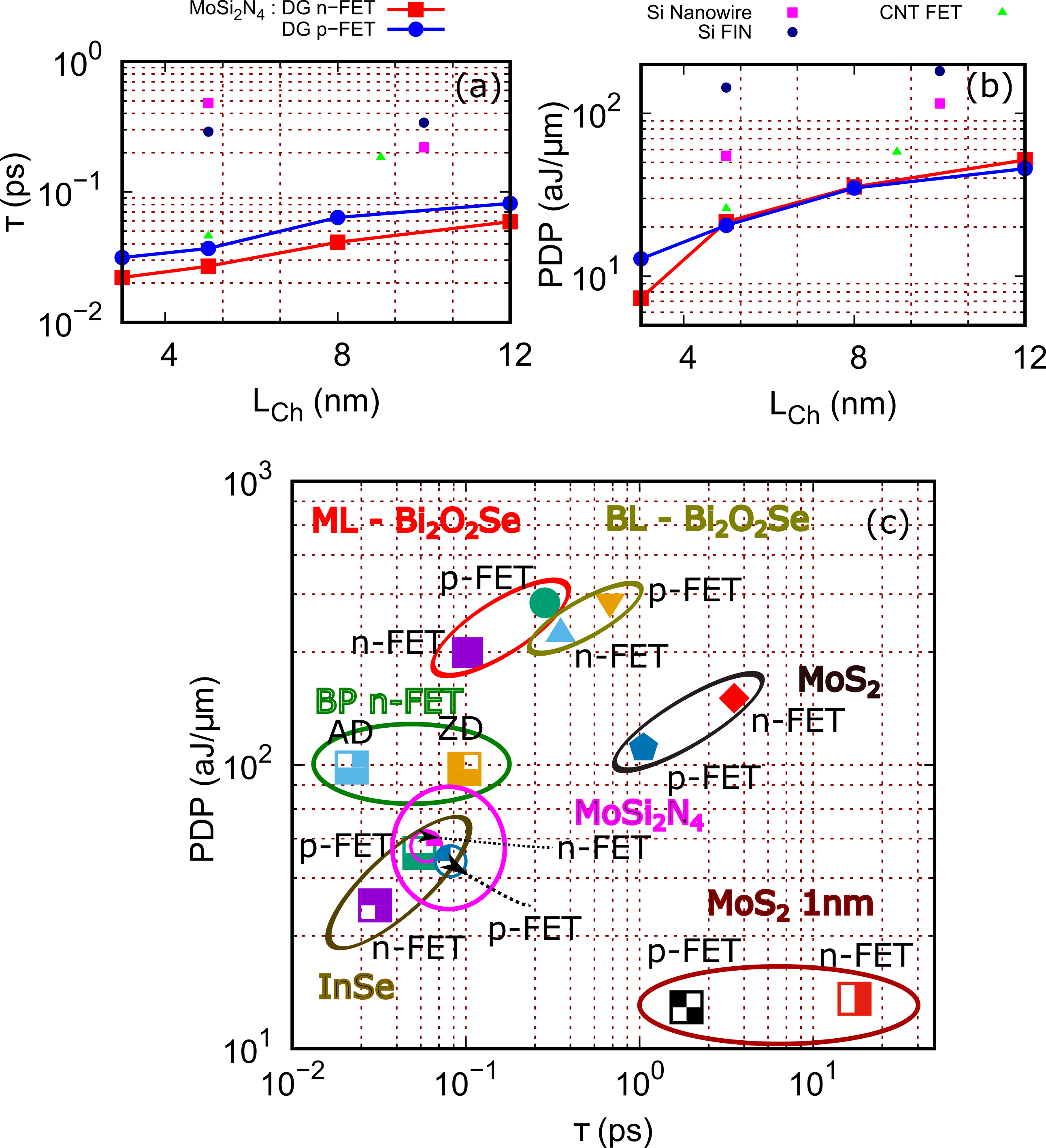
The delay and power dissipation product (PDP) are crucial figures of merits (FOMs) for logic applications. They determine switching speed and switching energy (energy per switching event), respectively. Figure. 10 (a) and (b) show the delay [] and PDP [] vs , respectively for DG FETs. These switching parameters for advance Si FETs (Si FinFETs[61, 62] and Si Nanowire FETs[63, 64]) and carbon nanotube (CNT) FETs[65, 66] are also shown in Fig. 10. For MoSi2N4 FETs with , and PDP lies in range and , respectively. Overall, MoSi2N4 FETs switch faster with lower switching energy than advance Si FETs (, ) and CNT FETs (, ). It is worth to notice that the theoretical limit on delay for non-tunneling barrier controlled binary logic switch is [63]. Our non-tunneling devices ( and ) have in the range .
The switching performance of DG MoSi2N4 based FETs () is benchmarked against other promising 2D materials based DG FETs[56, 58, 57, 52]. Other than 1 nm-MoS2 FET, the channel length of other 2D materials based FETs are in the range . The five best performing devices are BP AD n-FET, InSe n-FET, InSe p-FET, MoSi2N4 n-FET, and MoSi2N4 p-FET, these have energy-delay product (EDP = PDP ) (). The BP armchair direction (AD) n-FET has best switching speed among these, followed by InSe n-FET, InSe p-FET, MoSi2N4 n-FET, and MoSi2N4 p-FET. The MoS2 1nm- FETs have lower switching energy than others, but p-FET and n-FET are 23 times and 212 times slower than MoSi2N4 p-FET, respectively. The EDP of our devices are close to high performing InSe p-FET () and BP AD n-FET (). The best performing device is InSe n-FET with approximately one third EDP than our devices, and EDP of BP zigzag (ZZ) n-FET is approximately three times than our devices. Others (Bi2O2Se and MoS2) have EDP () far from MoSi2N4 FETs. All the devices have .
III-B3 FOMs of 32-bit Adder and ALU
The FOMs of a combinational (32-bit adder) and a sequential logic circuit (32-bit ALU) based on MoSi2N4 FETs are estimated, using the methodology of [60, 67]. The n- and p-type DG MoSi2N4 FETs with are considered, and are sized to deliver same current. The metal half pitch and contacted gate pitch are taken, which results in interconnect capacitance () = and interconnect delay () = for (HP applications).
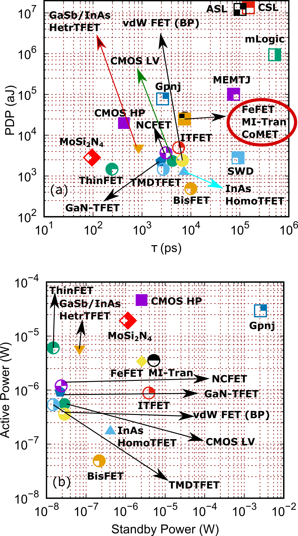
Using these data, the and are calculated for inverter with fan-out of four ( PDP = ), NAND gate with fan-in of four (), 32-bit adder (), and ALU () comprised of MoSi2N4 FETs. Figure 11 (a) and 12 (a) show vs for 32-bit adder and ALU, respectively based of MoSi2N4 and other spintronics and electronics logic devices (these data are taken from [67]). The spintronics devices (ASL, CSL, MEMTJ, mLgic, CoMET, and SWD) based adder and ALU switch slower and consumes more energy than electronics devices. Among electronics devices, switching speed of MoSi2N4 based adder and ALU is comparable to CMOS HP and ThinFET ( heterojunction interlayer TFET), but the switching energy of MoSi2N4 is one order less than CMOS HP and comparable to TFET devices (ThinFET and heterojunction TFET). Further, we characterize the power consumption parameters of adder and ALU. Figures 11 (b) and 12 (b) show the standby power vs. active power for adder and ALU comprised of MoSi2N4 FETs and other promising electronic devices. The standby power and active power of the circuits consisting of MoSi2N4 devices are close to CMOS HP and more than TFET devices (ThinFET and heterojunction TFET).

IV Conclusion
Two-dimensional semiconductors are promising candidates as a channel of next-generation electronic devices. In recent years, a new 2D semiconductor with the formula MoSi2N4 has been discovered and gaining attention owing to its excellent physical and electronic properties. In this work, the performance of FETs based on recently discovered ML-MoSi2N4 is assessed, using the first principles based quantum transport simulations. The upper-performance limit is reported, as the transport is assumed to be ballistic in nature. The scalability and impact of source-to-drain tunneling are investigated by performing channel length scaling study. The double-gate devices are scalable down to . However, the p-type devices are more immune to short channel effects (SCEs) than n-type. The performance is estimated as per the IRDS roadmap for the year 2034. The key FOMs for logic switches are calculated and benchmarked against other promising 2D materials-based FETs. It is found that the switching parameters of double-gate devices are better than advanced Si-FETs and CNT-based FETs. Finally, we calculate the FOMs of a combinational and a sequential logic circuit based on our double gate devices and benchmark against CMOS and beyond-CMOS logic technologies. The performance of 32-bit adder and ALU are promising among other alternative logic technologies.
Appendix
At each bias (), the transmission coefficient can be expressed as,
| (1) |
Here, and are retarded and advance Green functions, respectively. is the broadening from source/drain contacts. , , and can be expressed as,
| (2a) | |||
| (2b) | |||
| (2c) |
where, E and I are energy and identity matrix, respectively. (= +) is the sum of source and drain contact self-energy matrix, and H(k) is the channel Hamiltonian.
Next, the drain current () is calculated using the Landauer- approach[68]. For a given gate-to-source voltage () and drain-to-source voltage (), it can be expressed as,
| (3) |
where, is the electron charge, is the reduced Planck constant, = is the transmission coefficient at Energy for a given bias (, ), is the chemical potential at source/drain, and is the Fermi-Dirac distribution function at source/drain.
References
- [1] K. S. Novoselov, A. K. Geim, S. V. Morozov, D. Jiang, Y. Zhang, S. V. Dubonos, I. V. Grigorieva, and A. A. Firsov, “Electric field effect in atomically thin carbon films,” Science, vol. 306, no. 5696, pp. 666–669, 2004, doi: 10.1126/science.1102896.
- [2] K. S. Novoselov, D. Jiang, F. Schedin, T. J. Booth, V. V. Khotkevich, S. V. Morozov, and A. K. Geim, “Two-dimensional atomic crystals,” Proceedings of the National Academy of Sciences, vol. 102, no. 30, pp. 10 451–10 453, 2005, doi: 10.1073/pnas.0502848102.
- [3] K. S. Novoselov, “Nobel lecture: Graphene: Materials in the flatland,” Rev. Mod. Phys., vol. 83, pp. 837–849, Aug 2011, doi: 10.1103/RevModPhys.83.837.
- [4] M. Chhowalla, D. Jena, and H. Zhang, “Two-dimensional semiconductors for transistors,” Nature Reviews Materials, vol. 1, no. 11, p. 16052, Aug 2016, doi: 10.1038/natrevmats.2016.52.
- [5] S. Das, “Two dimensional electrostrictive field effect transistor (2D-EFET): A sub-60mV/decade steep slope device with High ON current,” Scientific Reports, vol. 6, no. 1, p. 34811, Oct 2016, doi: 10.1038/srep34811.
- [6] C. Qiu, F. Liu, L. Xu, B. Deng, M. Xiao, J. Si, L. Lin, Z. Zhang, J. Wang, H. Guo, H. Peng, and L.-M. Peng, “Dirac-source field-effect transistors as energy-efficient, high-performance electronic switches,” vol. 361, no. 6400, pp. 387–392, 2018, doi: 10.1126/science.aap9195.
- [7] N. Oliva, J. Backman, L. Capua, M. Cavalieri, M. Luisier, and A. M. Ionescu, “WSe2/SnSe2 vdW heterojunction tunnel FET with subthermionic characteristic and MOSFET co-integrated on same WSe2 flake,” npj 2D Materials and Applications, vol. 4, no. 1, p. 5, Apr 2020, doi: 10.1038/s41699-020-0142-2.
- [8] S. B. Desai, S. R. Madhvapathy, A. B. Sachid, J. P. Llinas, Q. Wang, G. H. Ahn, G. Pitner, M. J. Kim, J. Bokor, C. Hu, H.-S. P. Wong, and A. Javey, “MoS2 transistors with 1-nanometer gate lengths,” vol. 354, no. 6308, pp. 99–102, 2016, doi: 10.1126/science.aah4698.
- [9] Y.-L. Hong, Z. Liu, L. Wang, T. Zhou, W. Ma, C. Xu, S. Feng, L. Chen, M.-L. Chen, D.-M. Sun, X.-Q. Chen, H.-M. Cheng, and W. Ren, “Chemical vapor deposition of layered two-dimensional MoSi2N4 materials,” vol. 369, no. 6504, pp. 670–674, 2020, doi: 10.1126/science.abb7023.
- [10] A. Bafekry, M. Faraji, D. M. Hoat, M. Shahrokhi, M. M. Fadlallah, F. Shojaei, S. A. H. Feghhi, M. Ghergherehchi, and D. Gogova, “MoSi2N4 single-layer: a novel two-dimensional material with outstanding mechanical, thermal, electronic and optical properties,” Journal of Physics D: Applied Physics, vol. 54, no. 15, p. 155303, feb 2021, doi: 10.1088/1361-6463/abdb6b.
- [11] J. Yu, J. Zhou, X. Wan, and Q. Li, “High intrinsic lattice thermal conductivity in monolayer MoSi2N4,” New Journal of Physics, vol. 23, no. 3, p. 033005, mar 2021, doi: 10.1088/1367-2630/abe8f7.
- [12] B. Mortazavi, B. Javvaji, F. Shojaei, T. Rabczuk, A. V. Shapeev, and X. Zhuang, “Exceptional piezoelectricity, high thermal conductivity and stiffness and promising photocatalysis in two-dimensional MoSi2N4 family confirmed by first-principles,” Nano Energy, vol. 82, p. 105716, 2021, doi: 10.1016/j.nanoen.2020.105716.
- [13] R. Islam, B. Ghosh, C. Autieri, S. Chowdhury, A. Bansil, A. Agarwal, and B. Singh, “Tunable spin polarization and electronic structure of bottom-up synthesized MoSi2N4 materials,” arXiv preprint arXiv:2105.02739, 2021.
- [14] S. Gamage, Z. Li, V. S. Yakovlev, C. Lewis, H. Wang, S. B. Cronin, and Y. Abate, “Nanoscopy of black phosphorus degradation,” Advanced Materials Interfaces, vol. 3, no. 12, p. 1600121, 2016, doi: 10.1002/admi.201600121.
- [15] S. Ross and A. Sussman, “Surface oxidation of molybdenum disulfide,” The Journal of Physical Chemistry, vol. 59, no. 9, pp. 889–892, 1955, doi: 10.1021/j150531a020.
- [16] B. Radisavljevic, A. Radenovic, J. Brivio, V. Giacometti, and A. Kis, “Single-layer MoS2 transistors,” Nature Nanotechnology, vol. 6, no. 3, pp. 147–150, Mar 2011, doi: 10.1038/nnano.2010.279.
- [17] A. Nourbakhsh, A. Zubair, R. N. Sajjad, A. Tavakkoli K. G., W. Chen, S. Fang, X. Ling, J. Kong, M. S. Dresselhaus, E. Kaxiras, K. K. Berggren, D. Antoniadis, and T. Palacios, “MoS2 field-effect transistor with sub-10 nm channel length,” Nano Letters, vol. 16, no. 12, pp. 7798–7806, 2016, doi: 10.1021/acs.nanolett.6b03999.
- [18] F. Zhang and J. Appenzeller, “Tunability of short-channel effects in MoS2 field-effect devices,” Nano Letters, vol. 15, no. 1, pp. 301–306, 2015, doi: 10.1021/nl503586v.
- [19] I. Lee, J. N. Kim, W. T. Kang, Y. S. Shin, B. H. Lee, and W. J. Yu, “Schottky barrier variable graphene/multilayer-MoS2 heterojunction transistor used to overcome short channel effects,” ACS Applied Materials & Interfaces, vol. 12, no. 2, pp. 2854–2861, 2020, doi: 10.1021/acsami.9b18577.
- [20] D. Sarkar, W. Liu, X. Xie, A. C. Anselmo, S. Mitragotri, and K. Banerjee, “MoS2 field-effect transistor for next-generation label-free biosensors,” ACS Nano, vol. 8, no. 4, pp. 3992–4003, 2014, doi: 10.1021/nn5009148.
- [21] W. Liu, D. Sarkar, J. Kang, W. Cao, and K. Banerjee, “Impact of contact on the operation and performance of back-gated monolayer MoS2 field-effect-transistors,” ACS Nano, vol. 9, no. 8, pp. 7904–7912, 2015, doi: 10.1021/nn506512j.
- [22] X. Xie, D. Sarkar, W. Liu, J. Kang, O. Marinov, M. J. Deen, and K. Banerjee, “Low-frequency noise in bilayer MoS2 transistor,” ACS Nano, vol. 8, no. 6, pp. 5633–5640, 2014, doi: 10.1021/nn4066473.
- [23] B. Chakraborty, A. Bera, D. V. S. Muthu, S. Bhowmick, U. V. Waghmare, and A. K. Sood, “Symmetry-dependent phonon renormalization in monolayer MoS2 transistor,” Phys. Rev. B, vol. 85, p. 161403, Apr 2012, doi: 10.1103/PhysRevB.85.161403.
- [24] Y. Yoon, K. Ganapathi, and S. Salahuddin, “How good can monolayer MoS2 transistors be?” Nano Letters, vol. 11, no. 9, pp. 3768–3773, 2011, doi: 10.1021/nl2018178.
- [25] P. Rastogi, S. Kumar, S. Bhowmick, A. Agarwal, and Y. S. Chauhan, “Doping strategies for monolayer MoS2 via surface adsorption: A systematic study,” The Journal of Physical Chemistry C, vol. 118, no. 51, pp. 30 309–30 314, Dec 2014, doi: 10.1021/jp510662n.
- [26] C. Yadav, A. Agarwal, and Y. S. Chauhan, “Compact modeling of transition metal dichalcogenide based thin body transistors and circuit validation,” IEEE Transactions on Electron Devices, vol. 64, no. 3, pp. 1261–1268, 2017, doi: 10.1109/TED.2016.2643698.
- [27] C. Yadav, P. Rastogi, T. Zimmer, and Y. S. Chauhan, “Charge-based modeling of transition metal dichalcogenide transistors including ambipolar, trapping, and negative capacitance effects,” IEEE Transactions on Electron Devices, vol. 65, no. 10, pp. 4202–4208, 2018, doi: 10.1109/TED.2018.2855109.
- [28] K. Nandan, C. Yadav, P. Rastogi, A. Toral-Lopez, A. Marin-Sanchez, E. G. Marin, F. G. Ruiz, S. Bhowmick, and Y. S. Chauhan, “Compact modeling of multi-layered MoS2 FETs including negative capacitance effect,” IEEE Journal of the Electron Devices Society, vol. 8, pp. 1177–1183, 2020, doi: 10.1109/JEDS.2020.3021031.
- [29] B. Peng, D. Zhang, H. Zhang, H. Shao, G. Ni, Y. Zhu, and H. Zhu, “The conflicting role of buckled structure in phonon transport of 2D group-IV and group-V materials,” Nanoscale, vol. 9, pp. 7397–7407, 2017, doi: 10.1039/C7NR00838D.
- [30] G. Qin, Q.-B. Yan, Z. Qin, S.-Y. Yue, M. Hu, and G. Su, “Anisotropic intrinsic lattice thermal conductivity of phosphorene from first principles,” Phys. Chem. Chem. Phys., vol. 17, pp. 4854–4858, 2015, doi: 10.1039/C4CP04858J.
- [31] W. Li, J. Carrete, and N. Mingo, “Thermal conductivity and phonon linewidths of monolayer MoS2 from first principles,” Applied Physics Letters, vol. 103, no. 25, p. 253103, 2013, doi: 10.1063/1.4850995.
- [32] B. D. Kong, S. Paul, M. B. Nardelli, and K. W. Kim, “First-principles analysis of lattice thermal conductivity in monolayer and bilayer graphene,” Phys. Rev. B, vol. 80, p. 033406, Jul 2009, doi: 10.1103/PhysRevB.80.033406.
- [33] Q. Wang, L. Cao, S.-J. Liang, W. Wu, G. Wang, C. H. Lee, W. L. Ong, H. Y. Yang, L. K. Ang, S. A. Yang, and Y. S. Ang, “Efficient ohmic contacts and built-in atomic sublayer protection in MoSi2N4 and WSi2N4 monolayers,” npj 2D Materials and Applications, vol. 5, no. 1, p. 71, Aug 2021, doi: 10.1038/s41699-021-00251-y.
- [34] Q. Wu, L. Cao, Y. S. Ang, and L. K. Ang, “Semiconductor-to-metal transition in bilayer MoSi2N4 and WSi2N4 with strain and electric field,” Applied Physics Letters, vol. 118, no. 11, p. 113102, 2021, doi: 10.1063/5.0044431.
- [35] I. Souza, N. Marzari, and D. Vanderbilt, “Maximally localized Wannier functions for entangled energy bands,” Phys. Rev. B, vol. 65, p. 035109, Dec 2001, doi: 10.1103/PhysRevB.65.035109.
- [36] Y.-S. Lee, M. B. Nardelli, and N. Marzari, “Band structure and quantum conductance of nanostructures from maximally localized Wannier functions: The case of functionalized carbon nanotubes,” Phys. Rev. Lett., vol. 95, p. 076804, Aug 2005, doi: 10.1103/PhysRevLett.95.076804.
- [37] N. Marzari, A. A. Mostofi, J. R. Yates, I. Souza, and D. Vanderbilt, “Maximally localized Wannier functions: Theory and applications,” Rev. Mod. Phys., vol. 84, pp. 1419–1475, Oct 2012, doi: 10.1103/RevModPhys.84.1419.
- [38] IRDS 2020: https://irds.ieee.org/editions/2020.
- [39] G. Kresse and J. Furthmüller, “Efficient iterative schemes for ab initio total-energy calculations using a plane-wave basis set,” Phys. Rev. B, vol. 54, pp. 11 169–11 186, Oct 1996, doi: 10.1103/PhysRevB.54.11169.
- [40] P. E. Blöchl, “Projector augmented-wave method,” Phys. Rev. B, vol. 50, pp. 17 953–17 979, Dec 1994, doi: 10.1103/PhysRevB.50.17953.
- [41] J. P. Perdew, K. Burke, and M. Ernzerhof, “Generalized gradient approximation made simple,” Phys. Rev. Lett., vol. 77, pp. 3865–3868, Oct 1996, doi: 10.1103/PhysRevLett.77.3865.
- [42] A. A. Mostofi, J. R. Yates, G. Pizzi, Y.-S. Lee, I. Souza, D. Vanderbilt, and N. Marzari, “An updated version of Wannier90: A tool for obtaining maximally-localised Wannier functions,” Computer Physics Communications, vol. 185, no. 8, pp. 2309 – 2310, 2014, doi: 10.1016/j.cpc.2014.05.003.
- [43] S. Datta, Quantum transport: atom to transistor. Cambridge university press, 2005.
- [44] P. Rastogi, T. Dutta, S. Kumar, A. Agarwal, and Y. S. Chauhan, “Quantum confinement effects in extremely thin body germanium n-MOSFETs,” IEEE Transactions on Electron Devices, vol. 62, no. 11, pp. 3575–3580, 2015, doi: 10.1109/TED.2015.2477471.
- [45] T. Dutta, P. Kumar, P. Rastogi, A. Agarwal, and Y. S. Chauhan, “Atomistic study of band structure and transport in extremely thin channel InP MOSFETs,” physica status solidi (a), vol. 213, no. 4, pp. 898–904, 2016, doi: 10.1002/pssa.201532727.
- [46] K. Nandan, A. Agarwal, S. Bhowmick, and Y. S. Chauhan, “Performance investigation of p-FETs based on highly air-stable monolayer pentagonal PdSe2,” IEEE Transactions on Electron Devices, pp. 1–7, 2021, doi: 10.1109/TED.2021.3119552.
- [47] S. Li, W. Wu, X. Feng, S. Guan, W. Feng, Y. Yao, and S. A. Yang, “Valley-dependent properties of monolayer MoSi2N4, WSi2N4, and MoSi2As4,” Phys. Rev. B, vol. 102, p. 235435, Dec 2020, doi: 10.1103/PhysRevB.102.235435.
- [48] Y.-L. Hong, Z. Liu, L. Wang, T. Zhou, W. Ma, C. Xu, S. Feng, L. Chen, M.-L. Chen, D.-M. Sun, X.-Q. Chen, H.-M. Cheng, and W. Ren, “Chemical vapor deposition of layered two-dimensional MoSi2N4 materials,” Science, vol. 369, no. 6504, pp. 670–674, 2020, doi: 10.1126/science.abb7023.
- [49] M. Lundstrom and J. Guo, Nanoscale transistors: device physics, modeling and simulation. Springer Science & Business Media, 2006.
- [50] D. J. Griffiths and D. F. Schroeter, Introduction to quantum mechanics. Cambridge University Press, 2018.
- [51] D. Yin and Y. Yoon, “Can bilayer black phosphorus outperform monolayer in field-effect transistors?” in 2015 73rd Annual Device Research Conference (DRC), ser. 2015 73rd Annual Device Research Conference (DRC), 2015, doi: 10.1109/DRC.2015.7175614. . ISSN 1548-3770 pp. 177–178
- [52] F. Liu, Y. Wang, X. Liu, J. Wang, and H. Guo, “Ballistic transport in monolayer black phosphorus transistors,” IEEE Transactions on Electron Devices, vol. 61, no. 11, pp. 3871–3876, 2014, doi: 10.1109/TED.2014.2353213.
- [53] S. Zhang, S. Guo, Z. Chen, Y. Wang, H. Gao, J. Gómez-Herrero, P. Ares, F. Zamora, Z. Zhu, and H. Zeng, “Recent progress in 2D group-VA semiconductors: from theory to experiment,” Chem. Soc. Rev., vol. 47, pp. 982–1021, 2018, doi: 10.1039/C7CS00125H.
- [54] J. Wu, H. Yuan, M. Meng, C. Chen, Y. Sun, Z. Chen, W. Dang, C. Tan, Y. Liu, J. Yin, Y. Zhou, S. Huang, H. Q. Xu, Y. Cui, H. Y. Hwang, Z. Liu, Y. Chen, B. Yan, and H. Peng, “High electron mobility and quantum oscillations in non-encapsulated ultrathin semiconducting Bi2O2Se,” Nature Nanotechnology, vol. 12, no. 6, pp. 530–534, Jun 2017, doi: 10.1038/nnano.2017.43.
- [55] P.-H. Ho, Y.-R. Chang, Y.-C. Chu, M.-K. Li, C.-A. Tsai, W.-H. Wang, C.-H. Ho, C.-W. Chen, and P.-W. Chiu, “High-mobility InSe transistors: The role of surface oxides,” ACS Nano, vol. 11, no. 7, pp. 7362–7370, 2017, doi: 10.1021/acsnano.7b03531.
- [56] R. Quhe, J. Liu, J. Wu, J. Yang, Y. Wang, Q. Li, T. Li, Y. Guo, J. Yang, H. Peng, M. Lei, and J. Lu, “High-performance sub-10 nm monolayer Bi2O2Se transistors,” Nanoscale, vol. 11, pp. 532–540, 2019, doi: 10.1039/C8NR08852G.
- [57] Y. Wang, R. Fei, R. Quhe, J. Li, H. Zhang, X. Zhang, B. Shi, L. Xiao, Z. Song, J. Yang, J. Shi, F. Pan, and J. Lu, “Many-body effect and device performance limit of monolayer InSe,” ACS Applied Materials & Interfaces, vol. 10, no. 27, pp. 23 344–23 352, 2018, doi: 10.1021/acsami.8b06427.
- [58] J. Yang, R. Quhe, Q. Li, S. Liu, L. Xu, Y. Pan, H. Zhang, X. Zhang, J. Li, J. Yan, B. Shi, H. Pang, L. Xu, Z. Zhang, J. Lu, and J. Yang, “Sub 10 nm bilayer Bi2O2Se transistors,” Advanced Electronic Materials, vol. 5, no. 3, p. 1800720, 2019, doi: https://doi.org/10.1002/aelm.201800720.
- [59] Y. Wang, P. Huang, M. Ye, R. Quhe, Y. Pan, H. Zhang, H. Zhong, J. Shi, and J. Lu, “Many-body effect, carrier mobility, and device performance of hexagonal arsenene and antimonene,” Chemistry of Materials, vol. 29, no. 5, pp. 2191–2201, 2017, doi: 10.1021/acs.chemmater.6b04909.
- [60] D. E. Nikonov and I. A. Young, “Benchmarking of beyond-cmos exploratory devices for logic integrated circuits,” IEEE Journal on Exploratory Solid-State Computational Devices and Circuits, vol. 1, pp. 3–11, 2015, doi: 10.1109/JXCDC.2015.2418033.
- [61] D. A. Antoniadis, I. Aberg, C. N. Chleirigh, O. M. Nayfeh, A. Khakifirooz, and J. L. Hoyt, “Continuous MOSFET performance increase with device scaling: The role of strain and channel material innovations,” IBM Journal of Research and Development, vol. 50, no. 4.5, pp. 363–376, 2006, doi: 10.1147/rd.504.0363.
- [62] B. Doris, M. Ieong, T. Zhu, Y. Zhang, M. Steen, W. Natzle, S. Callegari, V. Narayanan, J. Cai, S. H. Ku, P. Jamison, Y. Li, Z. Ren, V. Ku, T. Boyd, T. Kanarsky, C. D’Emic, M. Newport, D. Dobuzinsky, S. Deshpande, J. Petrus, R. Jammy, and W. Haensch, “Device design considerations for ultra-thin SOI MOSFETs,” in IEEE International Electron Devices Meeting 2003, ser. IEEE International Electron Devices Meeting 2003, 2003, doi: 10.1109/IEDM.2003.1269360. pp. 27.3.1–27.3.4.
- [63] R. W. Keyes, “Fundamental limits in digital information processing,” Proceedings of the IEEE, vol. 69, no. 2, pp. 267–278, 1981, doi: 10.1109/PROC.1981.11959.
- [64] H. Iwai, “End of the scaling theory and Moore’s law,” in 2016 16th International Workshop on Junction Technology (IWJT), ser. 2016 16th International Workshop on Junction Technology (IWJT), 2016, doi: 10.1109/IWJT.2016.7486661. pp. 1–4.
- [65] S. E. Thompson and S. Parthasarathy, “Moore’s law: the future of Si microelectronics,” Materials Today, vol. 9, no. 6, pp. 20–25, 2006, doi: 10.1016/S1369-7021(06)71539-5.
- [66] A. Javey, J. Guo, Q. Wang, M. Lundstrom, and H. Dai, “Ballistic carbon nanotube field-effect transistors,” Nature, vol. 424, no. 6949, pp. 654–657, Aug 2003, doi: 10.1038/nature01797.
- [67] C. Pan and A. Naeemi, “An expanded benchmarking of beyond-CMOS devices based on boolean and neuromorphic representative circuits,” IEEE Journal on Exploratory Solid-State Computational Devices and Circuits, vol. 3, pp. 101–110, 2017, doi: 10.1109/JXCDC.2018.2793536.
- [68] M. Büttiker, Y. Imry, R. Landauer, and S. Pinhas, “Generalized many-channel conductance formula with application to small rings,” Phys. Rev. B, vol. 31, pp. 6207–6215, May 1985, doi: 10.1103/PhysRevB.31.6207.