Rosebud: Making FPGA-Accelerated Middlebox
Development More Pleasant
Abstract.
We introduce an approach to designing FPGA-accelerated middleboxes that simplifies development, debugging, and performance tuning by decoupling the tasks of hardware-accelerator implementation and software-application programming. Rosebud is a framework that links hardware accelerators to a high-performance packet processing pipeline through a standardized hardware/software interface. This separation of concerns allows hardware developers to focus on optimizing custom accelerators while freeing software programmers to reuse, configure, and debug accelerators in a fashion akin to software libraries. We show the benefits of the Rosebud framework by building a firewall based on a large blacklist and porting the Pigasus IDS pattern-matching accelerator in less than a month. Our experiments demonstrate that Rosebud delivers high performance, serving 200 Gbps of traffic while adding only 0.7–7 microseconds of latency.
1. Introduction
FPGAs have become the preferred platform on which to deploy in-network processing—middleboxes in particular—due to their flexibility: middleboxes perform a wide variety of network functions, many of which require hardware acceleration to function at today’s line rates. For example, intrusion detection systems (IDS) and SD-WAN middleboxes (Networks, 2023a) leverage hardware acceleration for signature matching (Networks, 2023c; Zhao et al., 2020) and supporting encrypted tunnels, respectively. Critically, FPGAs—as opposed to ASICs—also make it possible for vendors to update their middleboxes after deployment. For example, release notes from Palo Alto Networks indicate they have patched bugs in their deployed FPGA-based firewalls (Networks, 2023b).
Unfortunately, FPGA development is inherently intricate and laborious, and high-data-rate requirements only further complicate matters. Network link speeds have increased past 100 Gbps while FPGA clock rates remain plateaued, forcing middlebox developers to use resources more efficiently, which requires increasingly intricate knowledge of specific FPGA hardware elements to optimize their designs, including memory architecture, physical layout, and I/O. Additionally, FPGA development cycles are much longer than software because any change might break the logic that orchestrates packet processing, and there is much less visibility for debugging. Hence, despite their performance benefits, FPGAs have seen adoption for only a limited set of middlebox applications.
In this paper, we present the Rosebud framework for FPGA-based middlebox designs that simplifies development and debugging. At the heart of our framework is a new hardware abstraction we call a Reconfigurable Packet-processing Unit (RPU). RPUs are reconfigurable blocks within the FPGA fabric where we can drop in customized packet processing accelerators. RPUs are orchestrated in software by FPGA-resident RISC-V CPUs, as opposed to difficult-to-maintain hardware logic. Our key insight is that orchestration can be offloaded to (relatively) slow RISC-V CPUs yet still deliver overall line-rate processing. Additionally, this software-oriented framework makes it easier to debug and deploy accelerators because it enables software-driven debugging tools and supports hardware accelerator updates at runtime.
Realizing the RPU abstraction requires generalized supporting hardware. Specifically, Rosebud load-balances packets across parallel RPUs, implements a custom memory architecture to facilitate high-speed packet processing, and provides an interface between RPUs and the host. We implement Rosebud on top of a widely used Xilinx FPGA board and show that its area and latency overheads are marginal. We demonstrate that Rosebud can achieve 200 Gbps for popular middlebox applications including intrusion detection and firewalling. For instance, we used the Rosebud framework to port the engine of a state-of-the-art FPGA-based IDS implementation (Zhao et al., 2020) in less than 3 weeks, while adding runtime update capability to the IDS. Furthermore, we discuss how minor changes to one of the current FPGA families can further reduce the overheads, enabling additional slack for the developer and, in turn, simplify the development process.
This work makes the following contributions:
-
•
The RPU abstraction facilitates software-based development and debugging for FPGA-accelerated middleboxes.
-
•
We implement the Rosebud framework for load balancing middlebox workloads across packet processors, enabling coarse parallelism and no-pause reconfiguration.
-
•
We demonstrate that these development tools can be used to build 200-Gbps middleboxes much faster than with existing tools by porting the hardware accelerators of a state-of-the-art IDS to Rosebud, and making a firewall, in only one month.
Rosebud is open-source (Khazraee et al., 2023) and the source code is available at: https://github.com/ucsdsysnet/Rosebud. Appendix D provides instructions for how to reproduce the experiments in the paper.
2. Challenges
FPGAs have evolved to include features that make them attractive for high-speed middlebox applications, but these features require developers to forgo familiar software development paradigms for highly optimized FPGA hardware development. In this section we outline the key challenges developers face when implementing FPGA middleboxes and briefly describe how Rosebud addresses or alleviates them by empowering developers to focus on the accelerator design for their desired functionality.
2.1. Tailoring Logic to FPGA Platforms
Three features allow FPGAs to achieve line rate processing, but also increase the barrier to entry for developers. First, FPGA vendors tailor FPGAs for efficient high-speed packet processing. FPGAs now contain ASIC-like hardened logic for 100-Gbps Ethernet and PCI Express PHY/MAC. They also contain larger (e.g., 8) memory cells to enable buffering multiple packets, providing needed slack for complex, long-running packet processing tasks (e.g., managing different packet sizes) (Xilinx, 2016). However, these network-specific resources are provided as bare-bones hardware; middlebox developers need to understand exactly how they work and implement glue logic from scratch to meet their specific needs.
Second, manufacturers overcome FPGA clock-speed limitations by boosting fabric capacity (e.g., logic, memory, and I/O) through technologies that increase transistor density on FPGA chipsets (Trimberger, 2018) and employing multiple, interconnected FPGA dies. Middlebox developers can use these additional resources to increase throughput by parallelizing their implementations. In order to put available resources to best use, however, developers must provide hints to the heuristic-based FPGA development toolchain to help it achieve a feasible physical layout in the FPGA’s fabric.
Third, modern FPGAs can reconfigure a portion of their fabric while the rest of the logic continues to operate, enabling runtime updates. This technique, known as partial reconfiguration (PR), is well-suited for middlebox developers as it allows them to modify packet processing accelerators at runtime without any downtime. PR also enables developers to reach a full implementation by crafting a portion of the design as a static part, and adding on to the rest of the design incrementally. However, PR regions constrain the selection of the configurable regions in the fabric. Excluding these regions from the static part of the design also reduces the flexibility of resource selection and lowers total utilization. PR regions further require sophisticated border logic to avoid clock-frequency reduction, in addition to extra logic to ensure that the system remains stable during the reconfiguration. It requires a knowledgeable developer to minimize these overheads.
Rosebud hides the complexity of using platform-specific hardware by integrating them within the Rosebud runtime. Rosebud lays out partially reconfigurable regions based on the middlebox application’s needs and provides an optimized packet-distribution subsystem to fully addresses die-boundary-crossing challenges.
2.2. Orchestrating Parallel Units
While the increased real estate of modern FPGAs makes it possible to parallelize hardware accelerators to implement line-rate processing, it requires careful orchestration of the parallel units. There are two key challenges: (1) Different tasks take different amounts of time. For example parsing a packet’s header takes less time than finding a string in the payload. (2) Different tasks might also have different access patterns. For example, header processing uses a random access pattern and string matching uses streaming access. Designing the control logic to properly orchestrate the data flow among different accelerators is crucial—and one of the most fragile parts of the design, as a single cycle error in the control can cause corrupted data which is hard to track. Handling corner cases and exceptions further complicates this control logic.
Orchestration constraints further complicate updates to accelerators and limits reuse of third-party accelerators. A change to a single accelerator might break the orchestration among the accelerators and require multiple, long compile and debugging cycles to update the orchestration logic. Similarly, reusing third-party accelerators requires adapting their data flow and capabilities to match the rest of the design; designers are often better off reimplementing their own accelerators. Moreover, standardized hardware interfaces, such as AXI or AXI Stream (Xilinx, 2022), only provide connection for the accelerators; while separate orchestration logic is still required.
Rosebud enables use of software for fine-grained orchestration control. Our key insight is that orchestration tasks are relatively lightweight compared to accelerator operations, so they can be implemented in software running on wimpy cores. This also makes debugging orchestration easier as it can be scaffolded using familiar software-development tools.
Rosebud also supports course-grained parallelism by distributing packet processing across multiple parallel RPUs. Additionally, it provides a generic messaging system to address the communication needs among these parallel units.
2.3. Development and Debugging
FPGA development is slow. FPGA toolchains take hours to produce a bitstream for the FPGA image, and they offer limited debugging visibility (e.g., FPGA developers frequently debug their designs by looking at simulation waveforms); both significant limitations compared to software-based middleboxes that benefit from x86 programming and debugging tools. Some of these costs can be mitigated by simulating FPGA designs before building them, but simulations run much slower than real time—a few thousand packets can take on the order of hours to simulate, much slower than the millions of packets per second processed at operational line rates. Run-time debugging, which often is necessary because bugs can be missed in simulation, requires implementing extra debugging logic—with additional development iterations to hunt down the bug—which further prolongs development.
FPGA hardware development languages (i.e., HLS) have the potential to bridge the gap between software and hardware development; however, at its core HLS is just a tool that generates Verilog, so the developer needs to be fully aware of hardware restrictions and orchestration among different hardware modules. Furthermore, HLS designs are typically less performant than hand-crafted Verilog (Li et al., 2016). Also, HLS does not support software-like debugging tools, such as break points or memory dumping. It should be noted that developers can still use HLS-generated accelerators inside Rosebud’s packet processors for specific accelerator implementations, but need not employ it for the entire middlebox implementation. In Rosebud, use of software within FPGA at run time significantly simplifies the debugging process.
3. Processing Abstraction
We overcome the challenges presented in the previous section by introducing a new abstraction for middlebox packet processing accelerated by FPGA hardware, the Reconfigurable Packet-processing Unit (RPU). The RPU abstraction achieves the following goals: (1) reduce the required expertise needed to use networking-specific FPGA resources, (2) provide a way to incrementally update hardware accelerators and their orchestration, and (3) provide developers with visibility into hardware at runtime for debugging.
3.1. Reconfigurable Packet-processing Unit
An RPU consists of a RISC-V core connected to custom hardware accelerators, all residing inside a partially reconfigurable FPGA block. Packets are distributed across the RPUs using a customizable load balancer (LB). The software within each RPU is in charge of managing hardware accelerators to process packets; i.e., it orchestrates packet processing by invoking hardware accelerators as it would call functions in software. RPUs can be programmed using familiar C-based software abstractions for packet processing, such as packet descriptors for moving packets using a Direct Memory Access (DMA) engine. Figure 1 shows an overview of this abstraction. Lightweight processing, such as header parsing, can be implemented in software alone. To overcome the overhead introduced by the RPU’s software-based abstraction and to scale the performance of hardware accelerators, Rosebud implements a customized hardware load balancer that can be tailored to match the middlebox’s workload. The user can set the policy used by the LB unit, for example round robin, hash-based, or even a policy designed specifically for their target middlebox application.
The RPU abstraction provides all of the benefits of the software development cycle. For example, the software running on the RISC-V cores can inject or drop packets to see if a bug is being caused by them. It also can communicate with a host to provide samples of such packets or implement breakpoint behavior for certain conditions. Therefore, developers can identify and mitigate runtime issues by monitoring the state of accelerators and raising faults that either are handled directly on the software, or log errors and dump state, if desired on a per-packet basis, for a developer to inspect. RPUs can even handle doing this on a per-packet basis. In addition, software running on the host can dynamically update the hardware accelerators in an RPU at runtime using PR, and handle the required state transition in software, eliminating the need to design logic specifically to restore state after reconfigurations.
3.2. Software-Based Development Environment
Rosebud enables a developer to only focus on implementing their middlebox in a single RPU before they scale it to run at line-rate. The steps a developer needs to take to go from an idea to a full middlebox is as follows: (1) Write or choose their hardware accelerator and connect it within RPU. (2) Write the accompanying software to support the accelerator and compile it alongside the provided Rosebud libraries. (3) The developer can then test their entire software and hardware implementation in an RPU with a Python-based simulation framework. (4) After verifying the desired functionality, they can then build their RPU with the FPGA development toolchain. The Rosebud framework’s supporting hardware will already be placed and routed, including a block available for a custom LB module. (5) Finally, when the FPGA bitstream is ready, they can use Rosebud host-side C library and driver to load software and any constant data (e.g., lookup tables) to the RPU’s memory to be shared by the RISC-V cores and accelerators. This process is further detailed for the case study in Appendix A.
For developers, all supporting hardware is pre-made and pre-laid-out physically on the FPGA platform by Rosebud, allowing them to focus on the implementation of customized packet-processing software and hardware for their middlebox. For example, the packet-distribution system crosses die boundaries in a multi-die FPGA while still meeting high performance and low latency constraints. The design of the supporting hardware is described in Section 4.
3.3. Flexible Accelerator Orchestration
RPUs provide a well-defined interface for software and hardware to interact: the memory interface between the core and the accelerators. For instance, software can tell an accelerator what part of a packet to operate on by passing a pointer—using memory-mapped I/O—to the data’s location in the memory shared with the accelerators. As long as hardware and software follow the same memory-based interface, either can be changed without affecting the operation of the other. This effectively brings the commonly used embedded systems programming interface to FPGA middleboxes. The key insight that makes the RPU abstraction possible is the fact that orchestration takes much less time than the time it takes to process packets with hardware accelerators. However, achieving line-rate with this this abstraction requires a separate high-bandwidth packet distribution subsystem (Section 4.3).
3.4. Software-like Debuggability
An additional benefit of the RPU’s shared memory architecture is the ability to support software-driven hardware debugging. For runtime debugging, the host can communicate to different components of Rosebud. In particular, it has access to memory of each RPU to read and modify the state of accelerators, or even modify how the packets are being processed. The RPU achieves this by allowing developers to pause and reload software and memory in each RPU during runtime. Furthermore, the framework offers functionality similar to a breakpoint: RISC-V cores can set status registers that are readable by the host, and when those status registers change, they RPUs can simultaneously store some data in host memory, and enter a spin wait for the host to debug the problem. For example, if the packet distribution part of the Rosebud framework hangs, software on the RISC-V can detect the hang using internal timer interrupt, and send its state to the host. Furthermore, at runtime the host can send a poke interrupt to an RPU to tell it to stop processing packets, then the host can read the state of both the accelerators and RISC-V core by dumping the entire RPU shared memory.
Rosebud’s architecture also supports simulating an entire RPU’s operation, with or without the distribution system, avoiding the need to lay out a full design and deploy it to FPGA. We build a Python-based test bench framework based on Cocotb (cocotb, 2021). Developers can then link in the hardware accelerators and software they want to test, and run full simulation of the RPU’s operation. Another benefit of using Python is availability of several libraries, such as Scapy (Biondi and the Scapy community, 2022) to generate test cases. We also provide a Python library with the same API available between host and RPU.
4. Hardware Design
In this section we describe the hardware components in the Rosebud framework that enable the RPU abstraction. Figure 2 shows an overview of these components, and which part of the abstraction they support. We start by describing the hardware architecture of the RPU itself, namely the design of the shared-memory subsystem that enables seamless high-speed communication between the RISC-V core and the hardware accelerators. Then we describe the customizable, hardware load balancer that distributes packets across parallel RPUs to achieve line rates. Finally, we describe the high-rate packet switch that distributes packets to and from the external interfaces and host, and across the RPUs.
After introducing each component, we briefly overview the interface for the host to configure that component during runtime, if any. We also describe how we leverage features of middlebox applications to implement each component in a performant yet resource-efficient manner, without a significant decrease in performance or increase in latency over fully customized FPGA implementations. The components described in this section are all written in Verilog for Rosebud and come pre-laid out—and placed for the static portions—in the FPGA logic fabric.
4.1. RPU architecture
Each RPU contains two processing components, a RISC-V core and a set of accelerators. The RISC-V core and accelerators communicate over two memory-based interfaces: (1) a basic memory-mapped I/O for configuring and reading accelerator registers, and (2) a shared-memory subsystem that allows both the RISC-V core and accelerators to access and modify packets that are currently being processed. This shared memory also holds the state of both the RISC-V core (e.g., stack) and accelerators (e.g., scratch pad), as well as the instructions that the RISC-V core is executing.
We observe that accelerators and RISC-V cores have different ways of accessing memory. Accelerators usually read packet payloads in a streaming manner (e.g., word-by-word in sequence) to process the entire payload in order, and perform compute-heavy—i.e., relatively time-consuming—processing. As a result, accelerators benefit from using larger, higher-latency memories (e.g., Xilinx’s “Ultra-RAMs”) that can be pipelined to hide the latency while keeping up with line-rate throughput.
In contrast, RISC-V cores have more random accesses; for example parsing a header and deciding on the next field to read based on the output of that first read. This random read pattern is inefficient to support with higher-latency memories. Fortunately, the cores need to access the packet headers which require less data. As a result, we can copy the packet header and use smaller, lower-latency memories (e.g., BRAMs) for the RISC-V cores. This contrast provides an opportunity to design a tailored memory architecture.
Figure 3 shows an overview of the RPU’s memory architecture: we split the memory space into three parts. First, there are instruction and data memories of the RISC-V core (left) which are small and can be accessed within a cycle. Then, there is the large packet memory (center), where the packets arrive at from the packet distribution subsystem. This memory is shared between the RISC-V and accelerators, and can be used as a scratch pad. Finally, accelerators can have local memory loaded by the packet distribution subsystem for lookup tables or similar (right).
An interconnect module provides the interface between the RPU and the rest of Rosebud that distributes packets to the RPUs (Section 4.3). This module informs the RISC-V core about arriving packets by giving it descriptors, and the core can send packets back to the packet distribution framework by giving descriptors with the desired destination. The module also provides a control interface from the host to the RPU, for example, it can read and write the status registers, and interrupt the RISC-V.
The DMA engine inside the interconnect module has access to all these memories. This DMA engine is customized to copy an incoming packet to the shared packet memory, and also copy the packet header into the local RISC-V memory to parse the header with low latency. DMA engine can also be used to initialize the memories from the host—before booting the RISC-V core—to load lookup tables, or read them back for debugging purposes.
One limitation with FPGA memories is that they only have two ports. To avoid contention, local RISC-V memories have a dedicated port to the core, and the other port is used for the DMA engine to exchange packet-header data and facilitate low latency communication among RPUs (see Section 4.4). Since cores sparsely access the packet memory—e.g., for table look-up once per packet or for change a value in packets header—we share that port with the DMA engine and give higher priority to the core. This frees up the other packet memory port for the accelerators to have exclusive access. Finally,both ports of the local accelerator memory are dedicated to the accelerators at runtime, and only during boot or readback—where the accelerators are not active—the DMA engine can use one of the ports. For accelerator configuration or result readback, the RISC-V cores uses a separate memory mapped I/O (MMIO) channel to read/write the accelerators’ registers.
The RPU resides entirely inside a PR region, making it possible to swap it during run time. The RISC-V cores could have been implemented outside the RPU as part of the supporting architecture. However, due to the need for extra registers on the border of a reconfigurable region, it would increase the latency of RISC-V to the shared memories and accelerators. Moreover, by placing the RISC-V within the RPU, it leaves the option open for the developer to customize the core and tailor the core capabilities to their needs.
Interface between the host and the RPUs
We developed an API to provide the host-based control of RPUs (details in Section 3.2). In addition, there is an interface to use the partial reconfiguration process to load hardware in an RPU. First the host tells the LB not to send data to the specific RPU, then it waits for the packets within the RPU to drain. Next, it boots the RISC-V core in the updated RPU, and finally tells the LB to resume sending data to the RPU. We measured the time to pause, load the new bit file, and boot a new RPU, and it takes 756 milliseconds on average (across 320 loads).
4.2. Customizable Packet Load Balancer
For middleboxes, there is a clear load balancing opportunity to help scale the packet processing performance by using RPUs in parallel. Indeed, middleboxes often have load balancers that split the load between parallel servers. Use of a load balancer within an FPGA middlebox design results in (1) less burden of parallelism on the developer to achieve the desired performance, or in other words less load per RPU, (2) it enables laying out partially reconfigurable regions once and removing that burden from the developer, and (3) it enables reconfiguring one of the RPUs during runtime by configuring the LB to offload traffic to other RPUs. Developers can customize the LB policy to the application’s requirements, for instance one that assigns a new packet to the least-loaded core. We provide TCL scripts to make faster incremental builds when replacing the LB in the base FPGA image.
We leverage the packet-based data flow in middleboxes to simplify the developer’s design of the LB. In particular, the LB refers to packet memory in RPUs by a descriptor (slot number). Therefore, LB is only in charge of the load balancing policy and enforces it by labeling a packet with target RPU and memory slot. These slots are configured by the software running on RISC-V during boot, where it allocates some slots for packets and notifies the central LB about the number of slots and their maximum size. Similarly, communication between host DRAM and RPUs is also packetized, using a different slot number, i.e., DRAM tag.
After the LB has assigned a destination core for a packet, and that packet arrives at an RPU, the RPU’s interconnect (described in Section 4.1) notifies the RISC-V of an active descriptor. When sending out a packet, a RISC-V core has two options: it can ask the RPU interconnect to send it out directly, or it can tell the LB which slot is ready to be sent, and the LB will automatically send the transmit command to the interconnect. In both cases, the interconnect notifies the LB about slot being freed after it is sent out. By splitting the control functionality into a central part—the LB—and a distributed part—the interconnect, the slot abstraction also improves scalability of the system.
Interface between the host and LB
There is a read/write channel going from the host to the LB, with 30 bits of separate address space for writing and reading 32 bit words. The user can fully customize this channel to configure and control their LB during runtime. For instance, the developer uses this channel to select which cores are used for incoming traffic and which cores are disabled. They also can read the number of available slots inside the LB per RPU and other status registers. These data are helpful to detect freezes and starvation. Also the developer can use the host channel to prepare the LB for load of a new RPU by flushing the slots in the LB.
4.3. Packet Distribution
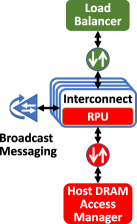
Figure 4a shows an overview of how packets flow from interfaces to RPUs. Incoming packets arrive at physical or virtual Ethernet interfaces, where they are assigned a destination RPU by the LB. There are two other sources and sinks interfaces for packets: (1) Host DRAM: used to move data over PCI-e to and from the host, and (2) loopback: used when an RPU wants to send a full packet to another RPU (Section 4.4). These two interfaces typically carry much less traffic than network-facing interfaces, so they can share the same infrastructure without sacrificing throughput.
As shown in Figure 4a, to make the packet distribution subsystem more resource efficient, switching is performed in two stages: first among four RPU clusters and then among the RPUs. This is to achieve the required performance with as little FPGA fabric resource utilization as possible. We implement a separate switch for each RPU cluster that has full throughput incoming, and four links running at 1/4th throughput outgoing. By using separate FIFOs for each incoming link inside this switch, the switch achieves non-blocking forwarding: each FIFO provides bit-width conversion without blocking the other incoming interfaces. Thus, the only necessary arbitration is when two input interfaces send to the same RPU. We use round-robin-policy arbitration by default; but it can be replaced with priority policy if desired. Also these switches are unidirectional and we have separate set of switches for incoming and outgoing traffic, not to block each other.
We were able to reduce the bit-width on the switches to each RPU by leveraging the fact that middleboxes do not have strict latency requirements. We can already tolerate latency of packets going over the PCIe bus in CPU-based middleboxes, as this latency is in the order of microseconds and it is negligible compared to packets traversing the Internet, which incurs latency on the order of milliseconds. Therefore, in Rosebud we only need to dedicate moderate bandwidth for data communication to each RPU to reduce the resource requirements of the packet distribution system, while still incurring less latency than going over the PCIe bus.
Each RPU’s interconnect is in charge of address handling and interfacing the packet distribution switch with the RISC-V core, as well as communicating to the LB and the host DRAM access manager. This coordination is facilitated by separate control channels for messages among RPUs and the LB, as well as request messages to host DRAM access manager. These control channels are separated from the data channels to avoid resource contention among them, and are shown in Figure 4b.
Interface between the host and packet distribution subsystem.
Hosts can read the status counters on all of the physical and virtual Ethernet interfaces, as well as each RPU. These counters contain the number of transferred bytes, frames, drops, or stalled cycles. They can shed light to how packets are going through the system, for instance how the LB is distributing packets. Therefore, they can reveal to the developer where the bottlenecks are located.
4.4. Inter-RPU messaging subsystem
Middlebox applications that require stateful packet processing might need to share state between parallel RPUs. This can be categorized into two types of message passing: (1) copying a packet or portion of memory to another RPU, or (2) sending a short message to update the state of the other processors (e.g., table). In a CPU-based middlebox, both of these can be implemented through cache coherency, but due to limited memory and the low clock rate on FPGAs, shared caches are inefficient and impractical to implement. In Rosebud, we design tailored messaging systems for these types of communication to make them more resource efficient.
For sending full packets between RPUs, we provide a loopback module that can route a packet between any two RPUs. The RISC-V cores can ask the LB for a packet slot from a destination RPU, and the packet can be transmitted using the same packet distribution subsystem. Inter-core packet messaging can also be used to implement a processing chain of heterogeneous RPUs with different accelerators and capabilities.
For sending short messages between RPUs, instead of using a full fledged coherent cache (with complex eviction and owner core capabilities) Rosebud features a simplified broadcast messaging system. A portion of memory is semi-coherent, where a write to this portion will eventually be propagated to all the other cores, and they all receive the message at the exact same time. This broadcast system is shown in Figure 4b. This design incurs less contention and overhead than a coherent cache. We further enable the use of interrupts to efficiently notify the receiving RPU regarding a message. The RISC-V program can configure the interrupts to be masked based on the target address. This can be used to send larger messages, where only the last word causes an interrupt, or to separate data and control messages. Rosebud further provides a FIFO for these notifications so as to not lose or reorder them.
5. Implementation
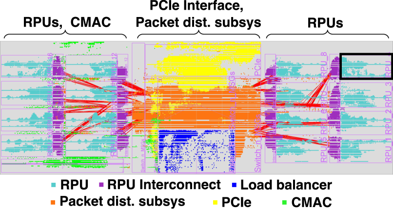
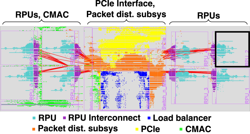
We implemented Rosebud on a Xilinx Virtex UltraScale+ FPGA VCU1525 board with an XCVU9P FPGA chip, shown in Figure 5 and Figure 6. There are 16 and 8 RPU versions respectively, where each RPU (cyan) has its own independent PR allocation as well as an RPU interconnect (purple) next to it for communicating to the rest of the system. We used the VexRISC-V 111https://github.com/SpinalHDL/VexRiscv as the core within each RPU. VexRISC-V is a small open source 32-bit RISC-V core with a 5-stage pipeline that is optimized for FPGAs. It also can be easily modified to select the developer’s desired capabilities.
| Component | LUTs | Registers | BRAM | URAM | DSP |
| Single RPU | 4541 (0.4%) | 3788 (0.2%) | 24 (1.1%) | 32 (3.3%) | 0 |
| Remaining (PR) | 23298 (2.0%) | 52132 (2.2%) | 12 (0.6%) | 0 | 168 (2.5%) |
| LB | 8221 (0.7%) | 22503 (1.0%) | 0 | 0 | 0 |
| Remaining | 70163 (6.0%) | 135897 (5.8%) | 144 (6.7%) | 48(5.0%) | 576 (8.4%) |
| Single Interconnect | 2793 (0.2%) | 2955 (0.1%) | 0 | 0 | 0 |
| CMAC | 6397 (0.5%) | 14849 (0.6%) | 0 | 18 (1.9%) | 0 |
| PCIe | 41526 (3.5%) | 63742 (2.7%) | 110 (5.1%) | 32(3.3%) | 0 |
| Switching | 86234 (7.3%) | 123654 (5.2%) | 48 (2.2%) | 64(6.7%) | 0 |
| Complete design | 259713 (22.0%) | 332636 (14.1%) | 542 (25.1%) | 626 (65.2%) | 0 |
| VU9P device | 1182240 | 2364480 | 2160 | 960 | 6840 |
We also allocated another larger PR block for the LB (blue). Our current load balancer implementations are basic and require very few resources, and the rest of the reserved area is empty for potentially a more sophisticated user LB. The main role of partial reconfigurability for the LB is to isolate its placement and routing, so if parameter updates to the LB are not sufficient, a developer can easily replace the LB. We do not support partial reconfiguration of LB during runtime, as it requires a backup LB module to switch to for the duration of the reconfiguration. The backup LB adds a significant resource overhead, while for many middlebox applications updates to the policy can be sufficiently expressed through passing parameters during runtime.
The physical Ethernet interfaces on the FPGA board are connected via MAC modules and FIFOs (green). The PCIe modules (yellow) are used for connecting to the host for control, accessing host DRAM, and providing a virtual Ethernet interface. Most of these components are provided by the Corundum open-source 100 Gbps virtual network interface (Forencich et al., 2020), which includes a driver for the Linux networking stack, enabling Rosebud’s operation as a NIC.
Finally, the packet distribution subsystem (orange) is connected to RPU interconnects (red lines show a few of these connections). The widest switches are 512-bits wide and the narrowest switches are 128-bits wide, they provide max throughput of 128 Gbps and 32 Gbps respectively. There is incurred overhead for switch arbitration that reduces their peak performance, but still the wider switches operate above 100 Gbps. We had to add several physical constraints to help Vivado (Xilinx’s FPGA development toolchain) in placement of the switches, as they are wide and span across the FPGA’s dies. After these optimizations, the switching infrastructure uses 54.7% of the FPGA’s die crossing registers.
Tables 1 and 2 show the utilization breakdown of the 8 and 16 RPU Rosebud runtimes for each of the main components, as well as the average resource utilization per RPU (without any accelerators). The table also shows the average remaining resources per PR block for each RPU, as well as the remaining resources in the LB block when using a round robin LB. Since the 8 RPU design has less arbitration logic than the 16 RPU design, we see less resource utilization. Across all implementations with all combinations of accelerators, including the case study accelerators, the maximum routing utilization in vertical or horizontal direction is 17%, and typically it is around 12%. The only hard IP blocks are the SERDES, PCIe and Gigabit CMAC; the rest are our own open source IP. We are able to meet timing at 250 MHz for all designs.
| Component | LUTs | Registers | BRAM | URAM | DSP |
| Single RPU | 4640 (0.4%) | 3806 (0.2%) | 24 (1.1%) | 32 (3.3%) | 0 |
| Remaining (PR) | 59521 (5.0%) | 125074 (5.3%) | 90 (4.2%) | 32 (3.3%) | 384 (5.6%) |
| LB | 7580 (0.6%) | 22076 (0.9%) | 0 | 0 | 0 |
| Remaining | 106436 (9.0%) | 208324 (8.8%) | 180 (8.3%) | 96(10.0%) | 648 (9.5%) |
| Single Interconnect | 2964 (0.3%) | 3051 (0.1%) | 0 | 0 | 0 |
| CMAC | 6396 (0.5%) | 14851 (0.6%) | 0 | 18 (1.9%) | 0 |
| PCIe | 41494 (3.5%) | 63734 (2.7%) | 110 (5.1%) | 32(3.3%) | 0 |
| Switching | 48402 (4.1%) | 68890 (2.9%) | 36 (1.7%) | 32(3.3%) | 0 |
| Complete design | 164699 (13.9%) | 224404 (9.5%) | 338 (15.7%) | 338 (35.2%) | 0 |
| VU9P device | 1182240 | 2364480 | 2160 | 960 | 6840 |
6. Evaluation
Next we evaluate the performance of the Rosebud framework. We ran several benchmarks to understand the limitations of different subsystems within Rosebud.
Experiment setup
Our experiments are conducted using a host with an Intel(R) Xeon(R) CPU E3-1230 V2 running at 3.3 GHz and a PCIe Gen 3 x16 expansion bus. We installed two separate Xilinx Virtex UltraScale+ FPGA VCU1525 boards into the PCIe bus, one serves as a traffic source/sink, while the other runs the system under test. Both ports of each FPGA are connected to the other FPGA, each with a 100-Gbps QSFP+ cable, totalling to a bandwidth of 200 Gbps. We use a round robin LB for this evaluation, as well as optimized bare-metal C code on the RISC-V processors to isolate software overhead from the overhead inherent to the framework.
6.1. Forwarding Throughput
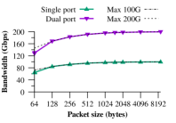
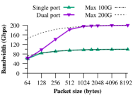
We tested the forwarding performance of the framework as a function of packet size. We consider packet sizes in the range of 64 to 8192 bytes by powers of two (excluding the 4-byte FCS), including the worst case of 65 bytes and the typical datacenter MTU packet sizes of 1,500 and 9,000 bytes. We sent packets from the tester FPGA interfaces and run a simple forwarder program on the RPUs to observe what portion of the packets are successfully forwarded. We use a 16 RPU design for the packet generation, and it saturates the maximum line rate of each packet size on the 200 Gbps link, other than for 64-byte packets which achieves 88% of the maximum rate at 200 Gbps (or 250 MPPS), and for 65-byte packets which achieves 89% of the maximum rate at both 100 Gbps and 200 Gbps (or 125 MPPS and 250 MPPS, respectively).
Figure 7 (a) and (b) show the maximum forwarding rate as a function of packet size for 16 and 8 RPUs respectively. The maximum theoretical effective rate is depicted as the dotted lines. Our 16 RPU implementation can forward at 100 Gbps for every packet size other than 64 bytes, where it achieves 88% of maximum rate (or 125 MPPS). For 200 Gbps, the 16 RPU implementation can forward at line rate for all packet sizes (note: below 128-byte, packets have reduced packet generation performance). For 8 RPUs, we perform similarly for 100 Gbps, but packets have to be at least 1024 byte packets to forward at the full 200 Gbps line rate.
The performance drop for 64 and 65-byte packets is primarily due to the RISC-V software latency in the RPUs. For instance, the minimum time for our packet forwarder to read a descriptor and send it back is 16 cycles. Therefore, each RPU forwards a packet every 16 cycles, and with 16 RPUs we can hit at most 250 MPPS (equal to the clock rate). Similarly, with 8 RPU design we reach a maximum packet rate of 125 MPPS. For the single port forwarding, our distribution subsystem is limited to 125 MPPS per incoming port limitation, which can be improved in the future.
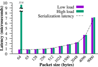
6.2. Forwarding Latency
Next, we measured Rosebud’s forwarding latency. Namely, the round trip time (RTT) from the traffic generator, through the FPGA under test, and back to the generator. To measure the latency, the packets are time-stamped just before leaving the packet generator, and the time is recorded upon arrival of them after the loopback. Figure 7c shows the measured latency for different packet sizes, both under low-load and maximum-load scenarios. The primary source of the measured delays is serialization. When a packet arrives at the FPGA and when it leaves the FPGA, MAC FIFOs add serialization latency at the line rate of each interface (i.e., 100 Gbps). Rosebud introduces additional serialization latency at 32 Gbps due to the fact that packet is fully loaded into each RPU’s shared memory before the RISC-V core is notified. The packets also have to be fully serialized on the way out of the RPU after the descriptor is released. The dotted line in Figure 7c shows the computed serialization delay according to the theoretical minimum latency given serialization (Equation 1). The 0.765sec in this equation corresponds to the minimum latency of packet forwarding through Rosebud, measured for the smallest packet size.
| (1) |
Since LB tracks the available slots in the RPUs, any packet past the LB can be absorbed by RPUs. Therefore, high load introduces only marginal additional latency, which likely comes from packets not being uniformly distributed between the two outgoing interfaces. The only exception is for 64-byte packets, where our packet generator can supply at a higher rate than what our packet forwarder can support, causing the receive FIFO to become full in steady state and add 32.8sec of additional latency.
6.3. Inter-RPU Messaging Performance
Finally, we measured the throughput of the inter-RPU loopback messaging system. Our implementation only uses a single 100-Gbps loopback port, since sending packets among cores for every incoming packet is not the intended design. To test the performance of this loopback port, we implement a two-step forwarding system: we assigned half of the RPUs to be recipients of the incoming traffic, and then each of these RPUs forwards packets to its corresponding RPU in the other half, and finally that core returns the packet to the link. We achieve 60% and 61% maximum throughput for the smallest packet sizes 64 Bytes and 65 Bytes respectively. Mainly Rosebud is bottlenecked by the destination RPU header having to be attached to each packet. For packet sizes larger than 128 bytes, the system can keep up with the full 100-Gbps line rate.
We also performed two tests to measure the latency of broadcast messages: one with a fixed-rate of sparse messages, and one where each RPU is trying to send as many messages as fast as it can. We time-stamp each message by writing the time-stamp value in the broadcast region, and upon arrival compare the current time against the transmit time. In the normal scenario of sparse messages, we observed a latency between 72 to 92 ns. When trying to send as many messages as possible—which is not the intended use for this communication channel—we observe 1,596–1,680 ns of latency for the design with 16 RPUs. This latency mostly comes from the 18 FIFO slots in each RPU—16 from actual FIFO and 2 from PR registers—which can be sent out every 16 cycles due to round-robin arbitration among cores (or every 8 cycles for the design with 8 RPUs). This accounts for 1,152 ns of this latency: cycles, each at 4 ns. A write to the broadcast memory region will be blocked until there is room in the FIFO. The rest of the latency is due to FIFOs and registers in the packet distribution subsystem and the RISC-V software having slight variations.
7. Case Studies
In this section we demonstrate how Rosebud can reduce development effort and time to build FPGA-accelerated middleboxes that can run at 200 Gbps. We show this with two case studies.
Case study 1: Porting Pigasus to achieve 200G
For our first case study, we ported Zaho et al’s Pigasus IDS (Zhao et al., 2020) to Rosebud. Pigasus is the first open source FPGA hardware design to achieve 100 Gbps throughput. We show that we can use the RPU abstraction to scale up the performance to twice the rate they achieved in their paper. The main questions we answer in this case study are as follows: How easily can we port the core Pigasus hardware accelerators—string and port matching—to Rosebud’s RPUs? Can we use Rosebud to achieve incremental hardware design where we start with a base accelerator and incrementally add improvements and observe their performance gain? Finally, how much the Rosebud framework can improve Pigasus’s performance?
Case study 2: Building a Blacklisting Firewall.
For our second case study, we evaluate how much easier Rosebud makes developing a new middlebox from scratch. Namely, we show it is feasible to implement a simple 200 Gbps firewall based on a single hardware accelerator that blocks packets that match an IP blacklist.
We were able to develop both of these case studies in less than a month in total by only one developer. We show Rosebud improved the line-rate of the Pigasus IDS from 100 Gbps to 200 Gbps for 800 Bytes packets222The average packet size for internet traces is over 800 Bytes (Zhao et al., 2020)., and achieves 200 Gbps for packets as small as 256 Bytes for the firewall implementation.
7.1. Pigasus IDS/IPS
7.1.1. Why is an IDS Hard to Develop in an FPGA?
IDSes identify suspicious behavior by monitoring network traffic and comparing it to a set of known fingerprints, stored in a constantly evolving ruleset. Many operators run all incoming traffic through an IDS, however they often have to divide traffic across clusters of servers to handle the computationally-intensive pattern matching for line-rate traffic (Heorhiadi et al., 2012). This computationally expensive operation is easy to parallelize; therefore, FPGAs are often considered for accelerating IDSes (Campbell and Lee, 2011; Weaver et al., 2007; Mitra et al., 2007). The Pigasus team built the first open-sourced FPGA-first IDS accelerator to provide 100 Gbps acceleration for the Snort IDS running on a single server (Zhao et al., 2020).
However, FPGA developers such as the Pigasus team had to build from scratch a significant fraction of their IDS hardware design to hit line-rate on an FPGA. The developers had to build their own packet processing pipeline from scratch, including building hardware accelerators for parts of the processing that could be done in software, such as packet parsing.
7.1.2. Porting Challenges and New Features
The details of the steps required to port Pigasus to Rosebud are provided in Appendix A. Unfortunately, in the first pass of building Pigasus with Rosebud, the scaled-up 200 Gbps design did not fit in our FPGA. After reaching out to the Pigasus team, they mentioned that lack of memory resources in the FPGA was a bottleneck for going to 200 Gbps, even when they used a large Intel Stratix 10 MX FPGA. However, upon a close look at our resource requirement report, we noticed that no large URAMs were used for the large lookup tables in string or port matcher accelerators. This is because URAMs cannot be initialized when an FPGA bitstream is loaded, as they are targeted for FIFOs. One method would be to initialize them during runtime, but before Rosebud that would have required more development effort to enable initialization from the server hosting the FPGA.
Using the RPU memory subsystem in Rosebud, we were able to fill these tables at runtime. We simply added a write port to the four large lookup memories in the accelerators. Still full Pigasus string matching engine did not fit in a single RPU, as they previously used the full FPGA for it. Fortunately, the number of string matching engines was parameterized, and by just changing it to 16 from 32, in addition to benefiting from the footprint reduction using URAMs, it fit within an RPU. The next highest utilization resource was the DSP blocks used for computing the hash for addressing the table, but it was still within the available capacity. We used the layout with 8 RPUs, as it provides more resources per RPU. A layout with 4 RPUs would have more resources per RPU, but the overhead of software running on RISC-V cores would become a bottleneck.
Rosebud also enabled overcoming a key limitation of the original Pigasus design: there is no way to reconfigure the pattern matcher’s ruleset during runtime. The only method to update the ruleset is to reload a new FPGA image. Not only we can benefit from the PR support in RPU, but also we can use the packet distribution subsystem to modify the large lookup tables during runtime.
| Component | LUTs | Registers | BRAM | URAM | DSP |
| RISCV core | 2048 (3.2%) | 1051 (0.8%) | 0 | 0 | 0 |
| Mem. subsystem | 3503 (5.5%) | 906 (0.7%) | 16 (14.0%) | 32 (50.0%) | 0 |
| Accel. manager | 803 (1.2%) | 2717 (2.1%) | 0 | 0 | 0 |
| Pigasus | 36012 (56.1%) | 49364 (38.3%) | 56 (49.1%) | 22 (34.4%) | 80 (20.8%) |
| Total | 42364 (66.0%) | 54037 (41.9%) | 72 (63.2%) | 54 (84.4%) | 80 (20.8%) |
| RPU | 64161 | 128880 | 114 | 64 | 384 |
| LB | 10467 (0.9%) | 24872 (1.0%) | 26 (1.2%) | 0 | 0 |
| Remaining | 103549 (8.8%) | 205528 (8.7%) | 154 (7.1%) | 96(10.0%) | 648 (9.5%) |
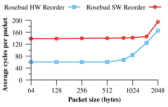
To further demonstrate the benefits of the bridging between software and hardware that Rosebud provides, we also implemented the Pigasus’s TCP flow reordering in software on the RISC-V core, instead of porting their hardware accelerator. We built a hash-bashed LB for Rosebud to always send packets of the same flow to the same RPU. The LB also pads the 4-byte hash result to the beginning of each packet, so that the software can reuse the flow hash without recomputation, and also know the exact hash that the LB has used. In each RPU, we used the scratch pad memory to keep 0.5 MB of flow state: storing the time and sequence number of the last seen packet from each flow, the flow hash, and the last 7 bytes of the packet required to be checked for the next packet. We can fit 32K entries of 16 Bytes within the 0.5 MB RPU memory, covering 15 bits of the hash as the index to this table. Since the LB has split the flows based on 3 bits of the same hash, in total we have covered 18 bits of the hash (out of 32 bits). Furthermore, older flows quickly time out in our software implementation, making a hash collision very unlikely. If we encounter reordering, we use up to half of our packet slots (e.g., 16) to buffer the out-of-order packets until the re-ordered packets arrive. In the rare case of collision, or running out of reordering buffers, we forward the corresponding packets to the host. Table 3 shows the average resource utilization break down inside each Pigasus RPU unit, as well as the hash-based LB used for this mechanism.
The software reordering will be less efficient than the hardware-based solution proposed in Pigasus, but utilizing software next to hardware can be used for prototyping or testing new ideas. To better understand the overhead of software reordering, we evaluate Rosebud assuming such hardware reordering accelerator exists within our round robin LB, similar to the inline hash computation accelerator within our hash-based LB. This is reasonable as their reassembler accelerator keeps the state per flow, and attaches the required state to each packet, so no state needs to be kept within RPUs and any RPU can process any packet. Since the addition of this accelerator would not impact the performance of software within RPUs, porting it was not necessary. However, compared to the numbers reported in the Pigasus paper, plenty of available resources still remain in our round robin LB (as shown in Table 2), should someone choose to add the reorder accelerator in the future.
7.1.3. Performance Evaluation
To evaluate the performance of Pigasus on Rosebud, we first made a packet trace based on the ruleset used for the generation of the Pigasus accelerator. Then, we used tcpreplay to transmit packets at low rate to verify that the expected number of packets are selected by the IPS accelerator and sent to the host. Next, using tcpreplay we played back the attack pattern, and used another FPGA to fill the rest of the pipe with background traffic to hit 200 Gbps. For this case study we ran the attack as 1% of the traffic (2 Gbps) with 0.3% reordering among the TCP flows in both the attack and safe traffic. This attack rate is considered a medium to high rate, and the reordering rate is the typical reordering happening for middlebox traffic (Zhao et al., 2020).
By using this traffic generation setup, we compared performance of three systems: (1) Pigasus with hardware accelerated reorder engine, (2) Pigasus with software reorder engine running on RISC-V cores, and (3) Snort running on a machine with Intel Xeon 6130 with 32 physical cores—or 64 hyper-threaded cores. For the Snort performance measurements, we setup the rules so Snort is performing only the exact same fast-pattern matching performed by the Pigasus accelerators. Also we enabled Snort’s Hyperscan (Wang et al., 2019) to improve fast pattern matching speed by benefiting from Intel’s AVX-512 vector instructions within Intel CPU, as well as the Linux Kernel’s AFPACKET 333https://doc.dpdk.org/guides/nics/af_packet.html to minimize the overhead for moving packets from the kernel to userspace. Enabling both of these resulting in more than 2 times improvement in performance.
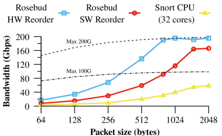
Figure 8a shows the results of this experiment. Rosebud with both hardware acceleration for both reordering and pattern matching achieves the highest performance: almost 200 Gbps for packet sizes larger than 800 Bytes. The use of software running on the slow RISC-V cores to do reordering does indeed lower performance, but it still can achieve almost 100 Gbps at 800 Bytes, and 166 Gbps for 2048 Byte packets. The non-perfect load balancing among the RPUs, due to non-uniformity of the flow hash results, also plays a smaller part in the performance degradation. Snort performs worse than both Rosebud implementations.
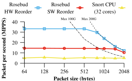
We also evaluate the performance differences from the perspective of packet rate (Figure 8b). The packet rate is limited by the software running on RISC-V cores in Rosebud to 60 and 138 MPPS for the HW-based and SW-based reodering, respectively. That is the limiting factor until 512 Byte packets for the HW-based reordering, and 1024 Bytes packets for the SW-based. After this thresholds, another limitation is added which is the maximum packet rate for a specific packet size at 200 Gbps, which is depicted by the dotted lines. For the HW-based reordering, from 800 Bytes packets the max packet rate is the dominant limiting factor and sets the performance, while for the SW-based results the software overhead still plays a part, even for 2048 Bytes packets.
For the Snort performance on a multi-core CPU, we see that for different packet sizes, the packet rate is limited between 4.7 and 5.6 MPPS. Although Snort is running on Xeon cores which have an order of magnitude higher clock rates than the FPGA, and Hyperscan hardware acceleration does speed up pattern matching on the multicore CPU, the achieved packet rate is much lower than Rosebud on an FPGA. This may be because Hyperscan’s acceleration is done in a sequential manner, even the AVX-512 instructions are not as fully pipelined, compared to the pattern matching in the Pigasus FPGA implementation. To make sure the Linux network stack is not introducing a bottleneck for Snort, we did an additional experiment where we ran Snort on only safe traffic with 2048 Bytes packets read directly from the RAM (Using ramdisk). The performance increased from 60 Gbps to only 70 Gbps, proving that AFPACKET moving packets between the interface and Snort is not the primary bottleneck for Snort’s performance. These results also clearly motivate why Pigasus can achieve ¿100 Gbps on a single host: the FPGA filters non-attack traffic coming in at line-rate, and the CPU only deals with attack traffic at a fraction of the line-rate.
7.1.4. Performance Analysis of Pigasus on Rosebud
Rosebud achieved twice as the performance of original Pigasus due to increased amount of parallelization. We used 16 string matching engines inside each RPU, as opposed to in the original Pigasus’s design. But we have 8 RPUs within our FPGA, that makes our system 4 times more parallel. Table 3 shows the resource utilization for this integration. As a point of comparison and benefits from using URAM memories, These 8 RPUs are placed within 2/3rd of our FPGA which in total has a similar capacity to their FPGA.
Considering that there were 8 RPUs and within each RPU the accelerators could potentially process 16 Bytes per cycle, the maximum rate for this computation at clock frequency of 250 MHz would be 256 Gbps. This is more than the target 200 Gbps performance, and hence not a bottleneck. However, as observed in Figure 8a the 200 Gbps is not achievable in many packet sizes. This results are also lower than the throughput of the packet distribution system, as shown in Section 6, indicating that packet distribution is not the bottleneck either. Indeed the software running on the slow RISC-V cores is setting the limit for small packet sizes.
Based on the measured packet rate, we can compute the number of cycles spent per packet, depicted in Figure 9. When no reordering is performed in the software (HW reorder line), the cycles spent per packet is 60.2 for the small packets. When we checked the simulation results for the same packet size and the same C-code, we observed that it takes 61 cycles for safe TCP packets, 59 cycles for safe UDP packets, and 82 cycles for attack traffic (the full code can be found in Appendix B). Therefore, on average, for 1% attack rate and a small portion of total packets being UDP, the measured results matches our simulation.
For hardware reordering, the software only runs the parsing and accelerator management, which could be fully parallelized with the Pigasus accelerator, therefore even for packet size 1024 Bytes which requires 61 cycles for Pigasus to process the payload, the simulation results were still 61 cycles, and only at 2048 Bytes did the Pigasus runtime become the bottleneck. That being said, for packet sizes 800 and above the maximum packet rate at 200 Gbps is bottleneck, not the software on RISC-V core.
For software reordering, the software needs to also handle the flow state table, resulting in more cycles spent per packet. The average cycles per packet starts from 138.4 cycles at 64 Bytes, and slightly rises until 1500 Bytes, where the line rate becomes the bottleneck and measurements do not reflect the software overhead anymore. This increase is due to less overlapping opportunity for the management software and the hardware accelerator, as starting off the Pigasus accelerator is dependent on the flow state table read results in software. For the software reordering case, the simulation results were not as consistent as before, but they were around the measured average value. To get a proper value it required potentially simulation of thousands of packets, which is not practical.
Additionally, during these experiments we learnt that careful software design and compiler efficiency plays a critical role to achieve high performance in Rosebud. For instance, for the implementation with hardware reordering, we obtained a 30% improvement in packet rate by adjusting the order of members in a struct, and also applying a bug fix from the latest RISC-V GCC which was not available on the Arch Linux repository version at the time.
7.2. Firewall
We next investigated how much developer effort is required to build a simple firewall middlebox from scratch using Rosebud. A firewall checks every single packet, and drops the packets whose IP matches a blacklist, otherwise they are forwarded to the other Ethernet interface.
To implement a firewall, we built a simple IP prefix lookup hardware accelerator from the list of 1050 blacklist IPs in the “emerging threats444https://rules.emergingthreats.net/fwrules/emerging-PF-DROP.rules” firewall rules. We wrote a basic python script to parse the rules and generate a Verilog code for the accelerator. This accelerator first checks for the first 9 bits of the IP prefix, if they match, then it checks for the remaining 15 bits in the next cycle, and if there was a match it raises a flag in a register. This lookup can be performed in only two clock cycles.
Then we assigned a register address that the RISC-V core could use to load the IP into the accelerator using MMIO, and another register to read the flag. Listing 1 shows a small code snippet from the RISC-V code to show how this works (the full code can be found in the Appendix C). We load the IP address from the Ethernet packet using the DMA descriptor pointer given by the RPU interconnect. Then we load the address into the IP matching accelerator (ACC_SRC_IP) and check the flag to see the results (ACC_FW_MATCH). In case of a match, we drop the packet by setting the descriptor length to 0; otherwise, we forward it by swapping the port value between 0 and 1; asking the packet distribution subsystem to send the packet to the other 100 Gbps port.
We were able to hit 200 Gbps for packets 256 Bytes and above, while injecting attack traffic within the background traffic. Table 4 shows the average resource utilization breakdown inside each firewall RPU unit. The resource consumption per firewall engine is small and for more number of rules, several such engines can be used in parallel and coordinated by the software.
| Component | LUTs | Registers | BRAM | URAM | DSP |
| RISCV core | 1976 (7.1%) | 1050 (1.9%) | 0 | 0 | 0 |
| Mem. subsystem | 2166 (7.8%) | 862 (1.5%) | 16 (44.4%) | 32 (100%) | 0 |
| Accel. manager | 518 (1.9%) | 1944 (3.5%) | 0 | 0 | 0 |
| Firewall IP checker | 835 (3.0%) | 197 (0.4%) | 0 | 0 | 0 |
| Total | 5493 (19.7%) | 4053 (7.3%) | 16 (44.4%) | 32 (100%) | 0 |
| RPU | 27839 | 55920 | 36 | 32 | 168 |
8. Related work
There has been a significant amount of prior work in developing FPGA-based NIC and also System-on-Chip (SoC) NIC development frameworks that are flexible and debuggable. However, no prior framework has addressed the issues for FPGA middleboxes, while providing a software like development and debugging, and the ability to change hardware acceleration—even during runtime.
8.1. FPGA Frameworks for NICs and Switches
This work builds on a large body of prior work on improving the software and hardware development process for FPGA-based NICs. However, they were not targeted at the specific developer needs of FPGA middleboxes. The HxDP (Brunella et al., 2022) framework, demonstrated a significant number of the development features could be provided by one framework. However, HxDP focuses on software-based compilation development environment for FPGAs and does not provide an interface to add new hardware accelerators to their framework; therefore it also does not provide a solution to parallelize custom accelerators. The PANIC (Lin et al., 2020) NIC framework has a similar packet distribution system to Rosebud; however, it does not provide software control over hardware accelerators, nor the software-like debugging. Also it is mainly targeted for ASIC implementations.
Other frameworks provide a well-defined shell on an FPGA to add custom accelerators (Gibb et al., 2007; Zilberman et al., 2014; Han et al., 2016; Firestone et al., 2018; Putnam et al., 2014; Li et al., 2016; Lavasani et al., 2012). However, none of these provided a software-based development process. There are also FPGA frameworks that are tailored for applications written in the P4 language (Wang et al., 2017; Pontarelli et al., 2019; Saquetti et al., 2020), but they are targeted for only switching applications rather than middleboxes, and do not provide software-oriented debugging capabilities like Rosebud. None of these prior frameworks demonstrated it was feasible to build a generic middlebox FPGA abstraction, like Rosebud, that can provide these features simultaneously and also achieve line-rate performance.
8.2. HW-Accelerated Network Applications
There are numerous projects that implemented hardware accelerated network middleboxes with their own custom FPGA hardware pipeline, including an ML platform (Ovtcharov et al., 2015), a key value store (Li et al., 2017), packet filtering (Vega et al., 2020), and several Intrusion Detection Systems (Mitra et al., 2007; Antichi et al., 2014; Weaver et al., 2007; Campbell and Lee, 2011; Wan et al., 2022). We believe that future efforts such as these may be bolstered by this platform. With Rosebud, developers will be able to focus on building their application-specific accelerators, and not have to manually tune a pipeline to get high-performance or manually build debugging hardware.
9. Conclusion and Discussion
Rosebud is a flexible and debuggable FPGA middlebox development framework. It provides a packet-processing abstraction consisting of a RISC-V core augmented with hardware accelerators, unified by custom tailored shared memory and packet distribution subsystems. We demonstrate that Rosebud can achieve 200 Gbps. We also demonstrate that Rosebud has a marginal effect on latency (especially when compared with PCIe and OS latencies). We plan to port Rosebud to several FPGA boards, from both Xilinx and Intel, to make it possible to use the same RPU abstraction among them. Rosebud can also be used for sharing FPGAs in the cloud services, such as Amazon AWS-F1 (Amazon, 2023), where the cloud provider controls the LB and users can load their logic into the RPUs. Finally, although FPGA-based middleboxes benefit most from the flexibility offered by Rosebud, we believe scope of Rosebud can be potentially wider. SoC-based SmartNIC designs can benefit from the memory and messaging subsystems to scale to higher link speeds. Fully custom ASIC designs can use Rosebud for their incremental builds where only the accelerators are updated between revisions.
Discussion: Rosebud on Hybrid FPGA platforms
A potential platform for Rosebud is SoC-like FPGAs with hardened CPUs, such as Xilinx Zynq UltraScale+ MPSoC (Xilinx, 2019). However, they have limited parallelism with a limited number of cores, small memory per core, and low incoming bandwidth ( Gbps per core). Most importantly though, they have high communication latency to the logic fabric ( ns (Xilinx forums, 2021a, b)) in the FPGA and use a generic shared bus that introduces contention, both of which critically limit their ability to orchestrate parallel processing in the accelerators. The RPU-based framework can be “hardened” in an SoC architecture in future FPGAs. Xilinx already has Network-on-Chip IP in their Versal family of FPGAs (Xilinx, 2020) that can save the resources used for packet distribution. AI cores available in this family are also similar to a software based processor, but they are not a full C-based core and also they are not spread across the programmable logic. Hardening the RISC-V cores will result in significantly faster packet processing performance, compared to the ones made on top of programmable logic. Rosebud already fully supports clock crossing between the core and accelerators domains. Furthermore, for applications that require large memories, the Versal family also includes FPGAs with integrated High Bandwidth Memory (HBM) up to 32 GB. If even larger memories are required, Rosebud can be mapped to Intel Xeon-FPGA hybrid chips (Cutress, 2018) to have faster access to host memory.
Acknowledgements.
We thank Manya Ghobadi for supporting this project while Moein was doing his postdoc at MIT. Also, we thank the anonymous reivewers for their detailed feedback. The MIT-affiliated author was supported by ARPA-E ENLITENED PINE DE-AR0000843, DARPA FastNICs 4202290027, NSF CNS-2008624, NSF SHF-2107244, NSF ASCENT-2023468, NSF CAREER-2144766, NSF PPoSS-2217099, NSF CNS-2211382, Meta faculty award, Google faculty award, Juniper Networks Sponsored University Research Initiative (SURI) award, and Sloan fellowship FG-2022-18504.Appendix A Steps to port Pigasus accelerator
In this appendix, we describe the steps to port a design to Rosebud, following our process for the Pigasus case study. We chose to port two of the main hardware accelerators from Pigasus: the pattern matcher, and the port matcher. As discussed in Section 7.1.2, we skipped porting their reassembly engine and modeled it by our round robin LB itself, while we replicated the functionality with a hash-based LB and use of software running on the RISC-V.
A.1. Developing the Accelerator
First, we simply copied the files in the string pattern matcher and port matcher directories from the Pigasus code base. We only had to swap a few IP modules—such as FIFOs—which were generated with Intel Quartus and were not compatible with Xilinx Vivado. We used our own libraries written in Verilog instead. Then we set the parameter for their rule packer module to output in chunks of 32 bits (rather than 128 bits) to match our RISC-V word size.
A.2. Connecting the Accelerator to RPU
Next, we had to write a basic wrapper to connect the Pigasus accelerators to the system within an RPU. The role of this wrapper is mainly to connect the wires and set the desired addressing for configuration registers. Their accelerators use a streaming input and could be connected directly within an RPU, as we support both the streaming data and random access memory—also known as native memory—interfaces. For the address assignment logic, it is a basic case statement in Verilog, and we provide examples for both blocking or non-blocking read and writes from the software running on RISC-V to the registers. Furthermore, to reduce the overhead of software control, we add basic hardware queues (FIFOs) per accelerator in this wrapper. Such queues make the orchestration of accelerators similar to an asynchronous scheduling software that manages local resources, where the software feeds and checks the accelerator resources.
A.3. Writing the Accompanying C Code
To have a complete RPU, we also need the software for the RISC-V processors to support the accelerators similar to a firmware. We use GNU RISC-V GCC to compile the code alongside the provided libraries to receive and send packets, and communicate with different components of Rosebud and the host. This code parses the packet headers, manages the Pigasus accelerator by feeding the start pointer and length of the payload, and finally appends the matched rule IDs to the matched packets before sending them to the host, or sends the safe traffic out on a physical port.
A.4. Simulating the C Code with Accelerators
At this stage, we can proceed to simulation to verify the interaction between the C code and the accelerators. We provide a Python-based simulation framework, using CocoTB (cocotb, 2021) simulator to connect Python to an RTL simulator for the Verilog code, Use of Python considerably simplifies writing test benches. For example, we could easily use Python libraries such as Scapy (Biondi and the Scapy community, 2022) to craft packets for testing, and also use idstools (Ish, 2022) to parse the rules and make the attack packets accordingly. To run the simulation, we provide Python functions to load the memories of the RPUs from the outputs generated by the GCC, as well as accompanying function to send and receive packets to the rest of the system. We provide both options of single RPU or full Rosebud simulation, the latter being more complete but also more time-consuming. At this stage, single RPU simulation proved to be more useful, as we were elaborating the interaction within an RPU, and also the packet distribution framework practically isolates the functionality of each RPU. The full Rosebud simulation can become handy to elaborate the design of a new LB, or communication between the RPUs if necessary.
A.5. Generating the Bitstream for FPGA
After verifying the functionality of the Pigasus accelerator within Rosebud, we proceeded to implementation with the FPGA development toolchain. We only needed to add the Verilog file names of the Pigasus accelerators, and the corresponding accelerator wrapper we developed, to our script and let the tool chain output the bit file for the target FPGA. Regions for RPUs are already laid out, and the rest of the logic is already placed and routed, so we only have to build the bitstreams for the partially reconfigurable regions of each RPU. After the first implementation run, we ran into the problem of insufficient resources per RPU. This issue was addressed through the additional capabilities provided in Rosebud framework, discussed in Section 7.1.2.
A.6. Load the FPGA and RPU Memories
Next, we loaded the bitstreams on the target FPGA, using our Bash scripts. We developed a host-side C library to communicate with the FPGA. This library integrates the Xilinx’s PR-loading tool, MCAP_tool, and the Corundum 100 Gbps FPGA-to-host NIC driver (Forencich et al., 2020). Therefore, we update an RPU using the PR-loading, and initialize the RPUs memories and LB configurations through C code running on the host. We used this library to load the instruction, data and accelerator memories of the RPU, directly from the ELF output file of GCC.
A.7. Runtime Debugging
For debugging, we use the host-side libraries where we have read and write access to the memories within an RPU, and we can send interrupts or read status bits from each RPU. We also developed a separate 64-bit debug channel between the host and each RPU. In a deadlock scenario, host can send a poke interrupt and communicate via an RPU in both directions using this channel at a lower rate.
A.8. Runtime Reconfiguration
To do reconfiguration of an RPU at runtime, we send a signal from the host to the LB to stop sending packets to that specific RPU, and then send an eviction interrupt to the RISC-V core to instruct it to finish processing the current packets and save the desired state to the host. Next we use the host-side libraries to write the new bit file to the PR block corresponding to the target RPU, followed by loading the RPU’s instruction and data memories. Now we reset the core and let it boot up, and restore its state by reading from the host memory if necessary. When the core is ready, we signal the LB through the host to resume sending packets to that RPU again.
Appendix B Code for Pigasus case study
The following code shows the C code running on the RISC-V cores for the Pigasus case study. This code is for the hardware reorder test and does not keep the flow state. The full code for the software reorder implementation can be found in the repository.
Appendix C Code for firewall case study
The following code shows the C code running on the RISC-V cores for the firewall case study.
Appendix D Artifact Appendix
D.1. Abstract
Rosebud is a framework to simplify development, debugging and performance tuning for FPGA-accelerated middleboxes. We have made all of the hardware designs (Verilog) and software (RISC-V C) open source on GitHub. The RISC-V toolchain and used python libraries are open-source. Building and programming the FPGA image requires Xilinx’s Vivado toolchain, however building the image take a long time and requires licenses from Xilinx, so we provide the bitstreams we used to run the experiments in the paper in the GitHub. A Makefile to generate FPGA bitstreams are provided, and also scripts to generate the host-side and RISC-V binaries.
The primary experiments in this work are evaluating the performance of Rosebud. Running these experiments requires running two Xilinx FPGA cards. The GitHub includes experiment scripts to evaluate Rosebud’s forwarding throughput and latency for different packet sizes. It also includes scripts, RISC-V software, and FPGA images to run the performance tests for the case studies of the Rosebud framework, including a firewall and an Intrusion Detection System (IDS). We include scripts to generate the packet traces for these experiments in GitHub. For each of the experiments we include a README that describes how to parameterize the Rosebud runtime environment for each data point in the experiments by passing parameters to a Makefile. We also include in the GitHub the software simulation framework that can be used to test the Verilog and RISC-V C for functional correctness.
D.2. Artifact Checklist (Meta-Information)
-
•
Run-time environment: Linux (tested on Ubuntu and Arch).
-
•
Execution: Load the Xilinx FPGA bitstreams running on two FPGA cards. Run experiment scripts.
-
•
Metrics: Throughput (i.e., packets per second), latency.
-
•
Output: We output the metrics for both the performance tests of the framework, as well as the case studies applications.
-
•
Experiments: We have provided scripts for the experiments. We expect minor variations from the results in the paper.
-
•
How much disk space required (approximately)?: The tests do not require considerable disk space, and 100 GBs for Vivado.
-
•
How much time is needed to prepare workflow?: An hour for installing open source tools, and a few for Vivado.
-
•
How much time is needed to complete experiments?: A few hours.
-
•
Workflow framework used?: We used Makefiles and bash scripts.
-
•
Archived (provide DOI)?: https://doi.org/10.5281/zenodo.7651655
D.3. Description
D.3.1. How to Access
-
•
Publicly available: https://github.com/ucsdsysnet/Rosebud
-
•
Code licenses: MIT License
D.3.2. Hardware Dependencies
-
•
Xilinx Virtex UltraScale+ FPGA VCU1525 (x2)
-
•
One or two machines hosting the FPGAs.
D.3.3. Software Dependencies
-
•
Xilinx Vivado 2022.2.1 and its drivers
-
•
riscv-gcc
-
•
Python3 alongside scapy, pyelftools, dpkt, idstools
-
•
tcpdump and tcpreplay
D.4. Installation
Steps to install required open-source software and Vivado drivers are mentioned in the repository.
-
•
Compilation: We have provided Makefiles for building the host-side binaries, driver, and RISC-V firmware.
-
•
Binary: FPGA images are provided.
D.5. Experiment Workflow
First, the FPGAs need to be programmed with the corresponding image. One FPGA is the tester FPGA that generates test packets, and one is the FPGA running benchmarks on the Rosebud framework, which we call the Design Under Test (DUT) FPGA. The tester FPGA is programmed with the Rosebud framework with a 16-RPU design and is mostly used as a high-speed packet generator. The DUT FPGA is programmed with different configurations of the Rosebud framework to benchmark it under a variety of test cases.
All of the experiments in this paper follow the same general procedure. First you will load the images on the FPGAs using a script we provide or Vivado. For instance, to load the image on the DUT FPGA that we use for most of the experiments, go to the directory host_utils/runtime and run:
If there are multiple FPGAs on the same machine, you can pass the JTAG index for the other FPGAs to this script, if this script fails you can use Vivado as a backup method to load the image.
Next, the Corundum Linux driver needs to be built and loaded. Go to host_utils/driver/mqnic and do:
Then reset the FPGAs after loading the driver, which can be done by running $ make reset_all from host_utils/runtime. If after programming, PCIe enumeration fails and host cannot see an FPGA (missing in output of make reset_all ), a system reboot and then reload of the Corundum driver is required (no need to reprogram).
To run code on the RISC-V cores on the FPGA, the corresponding binaries should be generated and loaded to the cores, alongside configuring the system settings (i.e., receiving RPUs). Finally, the host side profiling utility is run to measure the throughput of the system. These steps are scripted, e.g., in the make do command. All evaluation scripts are located in host_utils/runtime, and trace generation and injection scripts location are mentioned per each experiment. If both FPGAs are installed on the same machine, they can be addressed by their device names, e.g., mqnic0 and mqnic1.
D.6. Evaluation and Expected Results
In this evaluation, we assume both FPGAs are on the same
machine, where the mqnic0 device is the DUT FPGA and mqnic1
is the tester FPGA. For all experiments, we cross connect the 2 FPGAs with two
100G cables to enable 200 Gbps throughput between them, with the exception of
second step of the latency experiments.
Using the previous section commands, the tester and DUT FPGAs must be programmed with the 16 RPU packet gen bit file
(VCU1525_16RPU_Pktgen.bit), and the Firewall accelerator bit file
(VCU1525_16RPU_Firewall.bit) respectively. These images are sufficient to carry out all of the experiments except for the Pigasus case
study which requires a separate DUT image.
Packet forwarding throughput (Figure 7):
In two separate shells, go to host_utils/runtime and do:
The first command loads the packet forwarding firmware on the DUT FPGA, and the second command loads the basic packet generator that generates same size packets on the tester FPGA. For the packet generator FPGA we set the RPUs with incoming traffic to none (set RECV flag to 0), as we are only generating packets.
Now wait for the packets to flow for a minute to get a good average, and stop the process on the tester FPGA using Ctrl+C. The last print of the status table is the average values, and in the “RX bytes” field you can read the aggregate bytes per second for the physical and virtual Ethernet interfaces, which, on the DUT FPGA, shows how much data could be absorbed and processed. To test different packet sizes, you can stop both commands, and rerun them by changing the packet size argument for the tester FPGA. This is not necessary, but for more consistent results you can run $ make reset_all to reset the FPGAs before each test.
For the 8 RPU performance results, you can use the same 16 RPU setup and disable half of the clusters to achieve the same results. On the DUT FPGA side, run the following command:
On the tester side repeat the same process for different packet sizes. For 100 Gbps results, you can update the C code to use single port.
Packet forwarding latency (Figure 7):
To compute the forwarding latency, we timestamp the packets before sending them
from the tester FPGA, and after they arrive back after getting forwarded in the DUT
FPGA (timers in all RPUs are synced). This values are periodically sent to the
host. There is a second step that instead of using the DUT FPGA, we
cross-connect ports of the tester FPGA to measure the base latency and deduct it from the
latency measured in the first step.
For the first step, we load the forwarding code on the DUT FPGA:
We enabled half of the cores for receiving packets to be consistent with the single FPGA test in the next step, where half RPUs generate packets and half receive and report the results to the host. Throughout this experiment, we can keep the DUT FPGA running.
For the tester FPGA, from host_utils/runtime directory, run: 2$ ./run_latency.sh mqnic1
This script will loop through different packet sizes, for both low-load and maximum-load scenarios. It uses tcpdump to capture the latency samples that are sent to the host. After the script run is finished, you can use this command to extract latency values from the received pcaps and calculate the average latency per packet size and in each of the load levels: 2$ sudo ./latency_data_extractor.sh
For the second step of this experiment, we rewire the system to make it single tester FPGA loopback. Now we run the test script with a minor modification: 2$ ./run_latency.sh mqnic1 1l This saves the result in a different directory. We can rerun the latency_data_extractor.sh script as before to get the average values. The final deduction per point is done manually.
Firewall case study (number reported in Sec 7.2)
To regenerate the tester packet trace, you should run $ make gen in
fpga_src/accel/ip_matcher/python. This will create a trace based on the firewall
blacklist rules. In this trace, there are 1050 packets which are based on the blacklist, and 4
safe packets.
For the DUT FPGA, from host_utils/runtime run:
In another shell for the tester script and in the same directory run:
The pkt_gen code makes proper TCP/UDP packets and also can forward traffic from the host and inject it within the rest of the traffic. We set the BLOCK_INTS mask so that no traffic is received from the physical Ethernet ports.
Finally, to inject the attack traffic, in another shell go to
fpga_src/accel/ip_matcher/python and run:
This will inject the trace at about 5 Gbps. You can keep this packet injector running, and similar to the forwarding throughput experiment, stop the other two make do shells to observe the RX Bytes on the DUT FPGA, and set a different packet size for the tester FPGA. If make reset_all is used in any step, rerun the the injector script.
For application verification, on the tester FPGA you can run:
The tester FPGA will forward packets received from the host to the DUT FPGA, and the ratio of TX to RX frames shows the drop rate.
Intrusion detection system case study (Figure 8 & 9)
To generate the traces for this test, from
fpga_src/accel/pigasus_sme/python/ run:
For this experiment we need to reprogram the DUT FPGA, set the RPUs to 8 and load the RISC-V code. To get the HW reordering results, run this from host_utils/runtime:
For the tester FPGA, in another shell run:
Finally, for packet injection, from a third shell and from
fpga_src/accel/pigasus_sme/pcaps/ directory run:
This script will adjust the attack rate to be close to one percent.
Similar to the forwarding throughput experiment, you can pause the make do runs and check the RX bytes on the DUT FPGA.
For SW-based reordering, change the image and firmware and repeat the same testing process. From host_utils/runtime run:
The matched packets in this case study are sent to the host and can be seen with tcp_dump. Figure 9 results are extracted from the previous experiments in this subsection, by reversing the frame rate output to get the average cycles per packet.
Note that experiments can be customized by changing the packet size or attack traffic that is generated by the Python scripts.
References
- (1)
- Amazon (2023) Amazon. 2023. Amazon EC2 F1 Instances. https://aws.amazon.com/ec2/instance-types/f1/.
- Antichi et al. (2014) Gianni Antichi, Muhammad Shahbaz, Yilong Geng, Noa Zilberman, Adam Covington, Marc Bruyere, Nick Mckeown, Nick Feamster, Bob Felderman, Michaela Blott, Andrew W. Moore, and Philippe Owezarski. 2014. OSNT: Open Source Network Tester. IEEE Network 28, 5 (2014), 6–12. https://doi.org/10.1109/MNET.2014.6915433
- Biondi and the Scapy community (2022) Philippe Biondi and the Scapy community. 2022. Scapy: Packet crafting for Python. https://scapy.net/.
- Brunella et al. (2022) Marco Spaziani Brunella, Giacomo Belocchi, Marco Bonola, Salvatore Pontarelli, Giuseppe Siracusano, Giuseppe Bianchi, Aniello Cammarano, Alessandro Palumbo, Luca Petrucci, and Roberto Bifulco. 2022. hXDP: Efficient Software Packet Processing on FPGA NICs, In OSDI. Commun. ACM 65, 8, 92–100. https://doi.org/10.1145/3543668
- Campbell and Lee (2011) Scott Campbell and Jason Lee. 2011. Intrusion Detection at 100G. In State of the Practice Reports (Seattle, Washington) (SC ’11). Association for Computing Machinery, New York, NY, USA, Article 14, 9 pages. https://doi.org/10.1145/2063348.2063367
- cocotb (2021) cocotb. 2021. Cocotb, Python verification framework. https://www.cocotb.org.
- Cutress (2018) Ian Cutress. 2018. Intel Shows Xeon Scalable Gold 6138P with Integrated FPGA, Shipping to Vendors. https://www.anandtech.com/show/12773/intel-shows-xeon-scalable-gold-6138p-with-integrated-fpga-shipping-to-vendors.
- Firestone et al. (2018) Daniel Firestone, Andrew Putnam, Sambhrama Mundkur, Derek Chiou, Alireza Dabagh, Mike Andrewartha, Hari Angepat, Vivek Bhanu, Adrian Caulfield, Eric Chung, Harish Kumar Chandrappa, Somesh Chaturmohta, Matt Humphrey, Jack Lavier, Norman Lam, Fengfen Liu, Kalin Ovtcharov, Jitu Padhye, Gautham Popuri, Shachar Raindel, Tejas Sapre, Mark Shaw, Gabriel Silva, Madhan Sivakumar, Nisheeth Srivastava, Anshuman Verma, Qasim Zuhair, Deepak Bansal, Doug Burger, Kushagra Vaid, David A. Maltz, and Albert Greenberg. 2018. Azure Accelerated Networking: SmartNICs in the Public Cloud. In Proc. Symposium on Networked Systems Design and Implementation (NSDI) (Renton, WA, USA). USENIX Association, USA, 51–64.
- Forencich et al. (2020) A. Forencich, A. C. Snoeren, G. Porter, and G. Papen. 2020. Corundum: An Open-Source 100-Gbps NIC. In 2020 IEEE 28th Annual International Symposium on Field-Programmable Custom Computing Machines (FCCM). IEEE Computer Society, Los Alamitos, CA, USA, 38–46. https://doi.org/10.1109/FCCM48280.2020.00015
- Gibb et al. (2007) G. Gibb, J. Luo, J. W. Lockwood, G. Watson, J. Naous, P. Hartke, R. Raghuraman, and N. McKeown. 2007. NetFPGA–An Open Platform for Gigabit-Rate Network Switching and Routing. In 2007 IEEE Conference on Microelectronic Systems Education. IEEE Computer Society, Los Alamitos, CA, USA, 160–161. https://doi.org/10.1109/MSE.2007.69
- Han et al. (2016) Jong Hun Han, Noa Zilberman, Bjoern A. Zeeb, Andreas Fiessler, and Andrew W. Moore. 2016. Prototyping RISC Based, Reconfigurable Networking Applications. arXiv:arXiv:1612.05547
- Heorhiadi et al. (2012) Victor Heorhiadi, Michael K. Reiter, and Vyas Sekar. 2012. New Opportunities for Load Balancing in Network-Wide Intrusion Detection Systems. In Proc. of the 8th International Conference on Emerging Networking Experiments and Technologies (Nice, France) (CoNEXT ’12). Association for Computing Machinery, New York, NY, USA, 361–372. https://doi.org/10.1145/2413176.2413218
- Ish (2022) Jason Ish. 2022. py-idstools. https://github.com/jasonish/py-idstools/.
- Khazraee et al. (2023) Moein Khazraee, Alex Forencich, George C. Papen, Alex C. Snoeren, and Aaron Schulman. 2023. Rosebud_v1. https://zenodo.org/record/7651655.
- Lavasani et al. (2012) Maysam Lavasani, Larry Dennison, and Derek Chiou. 2012. Compiling High Throughput Network Processors. In Proceedings of the ACM/SIGDA International Symposium on Field Programmable Gate Arrays (Monterey, California, USA) (FPGA ’12). Association for Computing Machinery, New York, NY, USA, 87–96. https://doi.org/10.1145/2145694.2145709
- Li et al. (2017) Bojie Li, Zhenyuan Ruan, Wencong Xiao, Yuanwei Lu, Yongqiang Xiong, Andrew Putnam, Enhong Chen, and Lintao Zhang. 2017. KV-Direct: High-Performance In-Memory Key-Value Store with Programmable NIC. In Proc. of the Symposium on Operating Systems Principles (SOSP) (Shanghai, China) (SOSP ’17). Association for Computing Machinery, New York, NY, USA, 137–152. https://doi.org/10.1145/3132747.3132756
- Li et al. (2016) Bojie Li, Kun Tan, Layong (Larry) Luo, Yanqing Peng, Renqian Luo, Ningyi Xu, Yongqiang Xiong, Peng Cheng, and Enhong Chen. 2016. ClickNP: Highly Flexible and High-performance Network Processing with Reconfigurable Hardware. In Proc. ACM SIGCOMM (Florianopolis, Brazil) (SIGCOMM ’16). Association for Computing Machinery, New York, NY, USA, 1–14. https://doi.org/10.1145/2934872.2934897
- Lin et al. (2020) Jiaxin Lin, Kiran Patel, Brent E. Stephens, Anirudh Sivaraman, and Aditya Akella. 2020. PANIC: A Programmable High-Performance NIC for Multi-tenant Networks. In Proceedings of the 14th USENIX Conference on Operating Systems Design and Implementation (OSDI’20). USENIX Association, USA, Article 14, 17 pages.
- Mitra et al. (2007) Abhishek Mitra, Walid Najjar, and Laxmi Bhuyan. 2007. Compiling PCRE to FPGA for accelerating SNORT IDS. In Proc. of the ACM/IEEE Symposium on Architecture for Networking and Communications Systems (ANCS) (Orlando, Florida, USA) (ANCS ’07). Association for Computing Machinery, New York, NY, USA, 127–136. https://doi.org/10.1145/1323548.1323571
- Networks (2023a) Ethernity Networks. 2023a. SD-WAN Acceleration. https://ethernitynet.com/solutions/sd-wan-acceleration/.
- Networks (2023b) Palo Alto Networks. 2023b. All Release Notes. https://docs.paloaltonetworks.com/release-notes.html.
- Networks (2023c) Palo Alto Networks. 2023c. PA Series next generation firewalls - hardware architectures - PA7000. https://www.paloaltonetworks.com/resources/pa-series-next-generation-firewalls-hardware-architectures.
- Ovtcharov et al. (2015) Kalin Ovtcharov, Olatunji Ruwase, Joo-Young Kim, Jeremy Fowers, Karin Strauss, and Eric S. Chung. 2015. Toward accelerating deep learning at scale using specialized hardware in the datacenter. In 2015 IEEE Hot Chips 27 Symposium (HCS). IEEE, Cupertino, CA, USA, 1–38. https://doi.org/10.1109/HOTCHIPS.2015.7477459
- Pontarelli et al. (2019) Salvatore Pontarelli, Roberto Bifulco, Marco Bonola, Carmelo Cascone, Marco Spaziani, Valerio Bruschi, Davide Sanvito, Giuseppe Siracusano, Antonio Capone, Michio Honda, Felipe Huici, and Giuseppe Bianchi. 2019. FlowBlaze: Stateful Packet Processing in Hardware. In Proc. Symposium on Networked Systems Design and Implementation (NSDI) (USA). USENIX Association, USA, 531–547.
- Putnam et al. (2014) Andrew Putnam, Adrian M. Caulfield, Eric S. Chung, Derek Chiou, Kypros Constantinides, John Demme, Hadi Esmaeilzadeh, Jeremy Fowers, Gopi Prashanth Gopal, Jan Gray, Michael Haselman, Scott Hauck, Stephen Heil, Amir Hormati, Joo-Young Kim, Sitaram Lanka, James Larus, Eric Peterson, Simon Pope, Aaron Smith, Jason Thong, Phillip Yi Xiao, and Doug Burger. 2014. A Reconfigurable Fabric for Accelerating Large-Scale Datacenter Services. In Proceeding of the 41st Annual International Symposium on Computer Architecuture (ISCA ’14). IEEE Press, Minneapolis, MN, USA, 13–24.
- Saquetti et al. (2020) Mateus Saquetti, Guilherme Bueno, Weverton Cordeiro, and Jose Rodrigo Azambuja. 2020. P4VBox: Enabling P4-Based Switch Virtualization. IEEE Communications Letters 24, 1 (2020), 146–149. https://doi.org/10.1109/LCOMM.2019.2953031
- Trimberger (2018) Stephen M. Steve Trimberger. 2018. Three Ages of FPGAs: A Retrospective on the First Thirty Years of FPGA Technology. IEEE Solid-State Circuits Magazine 10, 2 (2018), 16–29. https://doi.org/10.1109/MSSC.2018.2822862
- Vega et al. (2020) J. Vega, M. Merlini, and P. Chow. 2020. FFShark: A 100G FPGA Implementation of BPF Filtering for Wireshark. In 2020 IEEE 28th Annual International Symposium on Field-Programmable Custom Computing Machines (FCCM). IEEE Computer Society, Los Alamitos, CA, USA, 47–55. https://doi.org/10.1109/FCCM48280.2020.00016
- Wan et al. (2022) Gerry Wan, Fengchen Gong, Tom Barbette, and Zakir Durumeric. 2022. Retina: Analyzing 100 GbE Traffic on Commodity Hardware. In Proc. ACM SIGCOMM. Association for Computing Machinery, New York, NY, USA, 530–544. https://doi.org/10.1145/3544216.3544227
- Wang et al. (2017) Han Wang, Robert Soulé, Huynh Tu Dang, Ki Suh Lee, Vishal Shrivastav, Nate Foster, and Hakim Weatherspoon. 2017. P4FPGA: A Rapid Prototyping Framework for P4. In Proc. of the Symposium on SDN Research (Santa Clara, CA, USA) (SOSR ’17). Association for Computing Machinery, New York, NY, USA, 122–135. https://doi.org/10.1145/3050220.3050234
- Wang et al. (2019) Xiang Wang, Yang Hong, Harry Chang, KyoungSoo Park, Geoff Langdale, Jiayu Hu, and Heqing Zhu. 2019. Hyperscan: A Fast Multi-pattern Regex Matcher for Modern CPUs. In Proceedings of the 16th USENIX Conference on Networked Systems Design and Implementation (Boston, MA, USA). USENIX Association, USA, 631–648.
- Weaver et al. (2007) Nicholas Weaver, Vern Paxson, and Jose M. Gonzalez. 2007. The Shunt: An FPGA-Based Accelerator for Network Intrusion Prevention. In Proc. of the ACM/SIGDA International Symposium on Field Programmable Gate Arrays (Monterey, California, USA) (FPGA ’07). Association for Computing Machinery, New York, NY, USA, 199–206. https://doi.org/10.1145/1216919.1216952
- Xilinx (2016) Xilinx. 2016. UltraRAM: Breakthrough Embedded Memory Integration on UltraScale+ Devices. https://docs.xilinx.com/v/u/en-US/wp477-ultraram.
- Xilinx (2019) Xilinx. 2019. Zynq UltraScale+ Device. https://www.xilinx.com/support/documentation/user˙guides/ug1085-zynq-ultrascale-trm.pdf.
- Xilinx (2020) Xilinx. 2020. Versal Premium ACAPs. https://www.xilinx.com/support/documentation/white˙papers/wp519-versal-premium-intro.pdf.
- Xilinx (2022) Xilinx. 2022. AMBA AXI4 Interface Protocol. https://www.xilinx.com/products/intellectual-property/axi.html.
- Xilinx forums (2021a) Xilinx forums. 2021a. Minimum Latency to Access Programmable Logic Register from ZYNQ ARM Core. https://support.xilinx.com/s/question/0D52E00007IPhkASAT/minimum-latency-to-access-programmable-logic-register-from-zynq-arm-core?language=en˙US.
- Xilinx forums (2021b) Xilinx forums. 2021b. Strategy for lowest latency to access AXI register. https://support.xilinx.com/s/question/0D52E00007IPiiCSAT/strategy-for-lowest-latency-to-access-axi-register?language=en˙US.
- Zhao et al. (2020) Zhipeng Zhao, Hugo Sadok, Nirav Atre, James C. Hoe, Vyas Sekar, and Justine Sherry. 2020. Achieving 100Gbps Intrusion Prevention on a Single Server. In Proceedings of the 14th USENIX Conference on Operating Systems Design and Implementation (OSDI’20). USENIX Association, USA, Article 61, 18 pages.
- Zilberman et al. (2014) Noa Zilberman, Yury Audzevich, G. Adam Covington, and Andrew W. Moore. 2014. NetFPGA SUME: Toward 100 Gbps as Research Commodity. IEEE Micro 34, 5 (2014), 32–41. https://doi.org/10.1109/MM.2014.61