Electrical transport properties of thick and thin Ta-doped SnO2 films
Abstract
Ta-doped SnO2 films with high conductivity and high optical transparency have been successfully fabricated using rf-sputtering method and their electrical transport properties have been investigated. All films reveal degenerate semiconductor (metal) characteristics in electrical transport properties. For the thick films ( with being the thickness) deposited in pure argon, the electron-phonon scattering alone cannot explain the temperature dependent behaviors of resistivity, the interference effect between electron-phonon and electron-impurity scattering should be considered. For the nm films, both conductivity and the Hall coefficient show linear relation with the logarithm of temperature () from 100 K down to liquid helium temperature. The behaviors of conductivity and Hall coefficient cannot be explained by the Altshuler-Aronov type electron-electron interaction effect, but can be quantitatively interpreted by the electron-electron interaction effects in the presence of granularity. Our results not only provide strong supports for the theoretical results on the electron-phonon-impurity interference effect, but also confirm the validity of the theoretical predictions of charge transport in granular metals in strong coupling regime.
I Introduction
Transparent conducting oxide (TCO) films possess both high conductivity and high optical transparency in the visible range, which render them to be widely used in the fields of flat panel displays, photovoltaic electrochromics, solar cells, and energy-efficient windows. [1, 2, 3, 4] Among various TCO films, SnO2-based films have long plasma wavelength, higher thermal stability, excellent durability, and higher mechanical hardness. [5, 6, 8, 7, 9] Thus they are the major industrial TCO films used in the fields of low-emissivity windows and solar cells. Currently, SnO2-based TCO films are mainly made of fluorine-doped SnO2 (FTO) and antimony-doped SnO2 (ATO) materials. [10, 11] For example, billions of square feet of FTO-coated window glass have been installed in buildings around the world. The architectural FTO films are generally deposited by spray pyrolysis method and their good conductivity is sacrificed for infrared radiation reflectivity and high visible transparency. [8, 12, 13] FTO or ATO film with high conductivity is usually prepared by chemical vapour deposition techniques and not suitable to be deposited by sputtering methods. [14, 15, 16, 17, 18] Thus to explore SnO2-based TCO films which could be fabricated by sputtering deposition is nontrivial.
Recently, the first-principle calculation results[19, 20, 21, 21] indicate that Ta-doped SnO2 (Ta:SnO2) reveals degenerate semiconductor characteristics in electronic structure and its optical bandgap is wider than that of the undoped SnO2. It means that Ta:SnO2 could reveal metallic characteristics in transport property and remain visibly transparent. Using a target composed of mixture of SnO2 and Ta2O5, one can fabricate Ta:SnO2 film via rf-sputtering method. Thus it is necessary to investigate the influences of deposition conditions on the resistivity and optical transparency of the deposited films. In addition, to understand the conduction mechanisms, it is essential to investigate the temperature dependence of the resistivity and Hall coefficient of the material. In this paper, Ta:SnO2 films are successfully fabricated using rf-sputtering technique and the deposition conditions including substrate temperature and sputtering atmosphere are researched and optimized. The electrical transport properties for films with thickness ranging from 1000 to 10 nm are systematically investigated.
II Experimental method
Our films were deposited on (0001) Al2O3 single crystal substrates by standard rf-sputtering method. Besides higher melting point, Al2O3 single crystal possesses relatively higher thermal conductivity, which makes the thermal equilibrium between the film and sample holder more easy in electrical transport measurements. The sputtering source was a commercial ceramic target of SnO2 (99.9%) and Ta2O5 (99.99%) mixture, in which the atomic ratio of Ta to Sn is . The base pressure of the depositing chamber was less than Pa, and the deposition was done at 0.6 Pa in a mixture of argon and oxygen atmosphere. Four films with thicknesses 1 m were first deposited at , 953, 963, and 983 K ( is the substrate temperature), respectively. During the deposition, the sputtering power was maintained at 150 W and the volume ratio of oxygen to argon was set to zero. It was found that the resistivity of film deposited at 963 K was less than that of other films at a certain measured temperature. Thus the substrate temperature is kept at 963 K in the subsequent deposition processes. The volume ratio of oxygen to argon and oxygen () was then adjusted between 0 and 2.0% and it was found that was the optimal ratio in terms of the conductivity and optical transparency of the film. Finally, Ta:SnO2 films with thickness ranging from 11 to 36 nm were deposited at the optimized condition ( K and ).
The thicknesses of the nm films were measured using a surface profiler (Dektak, 6M), while the thicknesses of the nm films were evaluated through growth rate and deposition time. The crystal structure and quality of the films were determined by x-ray diffraction (XRD, Rigaku D/MAX-2500). Optical absorption and transmittance spectra were measured in a UV-VIS-NIR spectrometer (Hitachi V4100). The resistivity and Hall coefficient were measured in a physical property measurement system (PPMS-6000, Quantum Design) using the four-probe method. Hall-bar shaped samples, defined by mechanical masks, were used for the resistivity and Hall effect measurements.
III Results and Discussion
III.1 Crystal structure and optical transparency
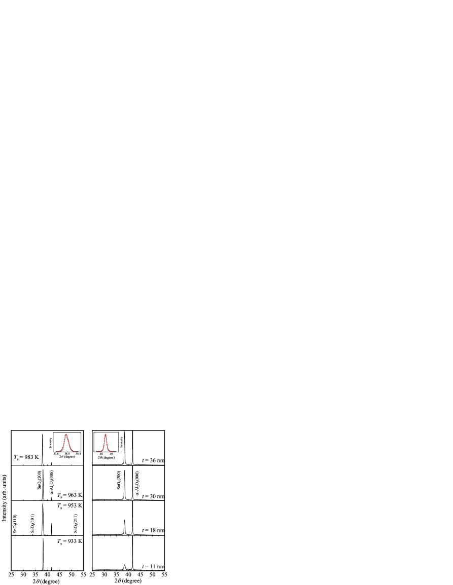
Our samples are split into two groups. The films with thickness nm are called thick films, while these nm ones are called thin films. Figure 1 shows the XRD patterns for some representative films. The deposition condition and the thickness of each film are labeled in the figure. The diffractions can be indexed based on the structure of undoped tetragonal SnO2 (powder-diffraction file number: 46-1088). From the left panel of Fig. 1, one can see that the peaks related to the diffractions of (1 1 0), (1 0 1), (2 0 0), and (2 1 1) planes of tetragonal SnO2 appear in the patterns for films deposited at 933 K and 953 K. While for the films deposited at K, only the diffraction of (2 0 0) plane can be observed. Other impurity phases such as Ta2O5 or Ta-Sn alloys (compounds) are not detected. The thin films deposited at 963 K retain the texture-growth feature (along [1 0 0] direction), even when the thickness of the film is as low as 11 nm. For the thick films, it is found that the film deposited at K has the minimum resistivity at a certain fixed temperature. Thus we take K as the optimal substrate temperature.
The mean grain size of each film was determined from the full width at half maximum (FWHM) of (2 0 0) diffraction peak using Scherrer’s equation[22, 23, 24, 25]
| (1) |
where is the mean diameter of the grains, is the x-ray wavelength, is the FWHM of the selected diffraction peak, is the diffraction angle, and is a constant. The FWHM of (2 0 0) peak can be evaluated by fitting the experimental data to Gaussian function (see the inset of Fig. 1). Taking , [22] we calculate the mean grain sizes of the films and list them in Table 1. For the thin films, the mean grain size increases as the thickness of the films increases, while the mean grain size increases with increasing for the thick films. The mean grain sizes of the thick films were also measured by a scanning electron microscope. It is found that the difference of the mean sizes determined by the two methods is less than 10%.
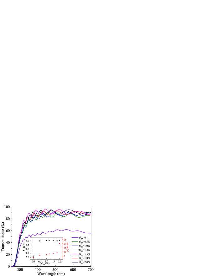
Figure 2 shows the optical transmittance () as a function of wavelength for films deposited at K and different oxygen partial pressure (), as indicated. Here is the intensity ratio of transmitted light to incident light, and the thicknesses of these films are in the range of 550 to 1000 nm. For the film deposited in pure argon, the transmittance in the visible range is less than 60%, while for these deposited at O2 and Ar mixture, the transmittance is greater than 85%. From Fig. 2, one can get the optical absorption coefficient via with being the thickness of the film. According to Tauc et al., [26] the relation between and the incident photo energy is , where for a direct transition and for an indirect transition, is a constant, and is the optical band gap. According to the first-principle calculation result, [20] Ta:SnO2 is a direct gap degenerate semiconductor, thus the value of of each film can be obtained by extrapolating the linear part of versus plot to . The inset of Fig.2 shows versus the oxygen partial pressure for these Ta:SnO2 films. The optical band gap is 3.9 eV for the film deposited at pure argon atmosphere. When 0.5% oxygen is introduced, increases to 4.6 eV and then almost keeps as a constant with further increasing oxygen percentage. The inset of Fig. 2 also gives the resistivity versus oxygen partial pressure measured at 300 K. The resistivity increases with increasing in the whole testing range. Combining the oxygen partial pressure dependence of optical transmittance and resistivity, one can see that the optimum oxygen percentage is . Thus the optimal depositing conditions for Ta:SnO2 film with both high conductivity and high optical transparency are K and in our sputtering system.
| (300 K) | |||||||||||
|---|---|---|---|---|---|---|---|---|---|---|---|
| Films | (nm) | (K) | (nm) | ( m) | ( m) | (n m K-1) | (10-7 K-2) | (K) | (m-3) | ||
| 1 | 958 | 983 | 47.3 | 4.46 | 4.23 | 4.81 | 1.31 | 1024 | |||
| 2 | 992 | 963 | 36.9 | 3.16 | 2.90 | 4.07 | 5.72 | 1116 | |||
| 3 | 962 | 953 | 34.2 | 4.56 | 4.35 | 4.55 | 0.94 | 1080 | |||
| 4 | 960 | 933 | 26.2 | 3.93 | 3.69 | 4.25 | 2.66 | 1061 | |||
| 5 | 36 | 963 | 31.6 | 8.85 | 8.53 | 3.75 | 24.02 | 2.12 | |||
| 6 | 30 | 963 | 24.2 | 10.93 | 10.64 | 3.22 | 14.84 | 1.46 | |||
| 7 | 18 | 963 | 17.7 | 10.25 | 9.96 | 2.95 | 10.38 | 1.64 | |||
| 8 | 11 | 963 | 9.8 | 13.04 | 12.9 | 3.09 | 4.94 | 1.66 |
III.2 Electron-phonon-impurity interference effect in the thick films
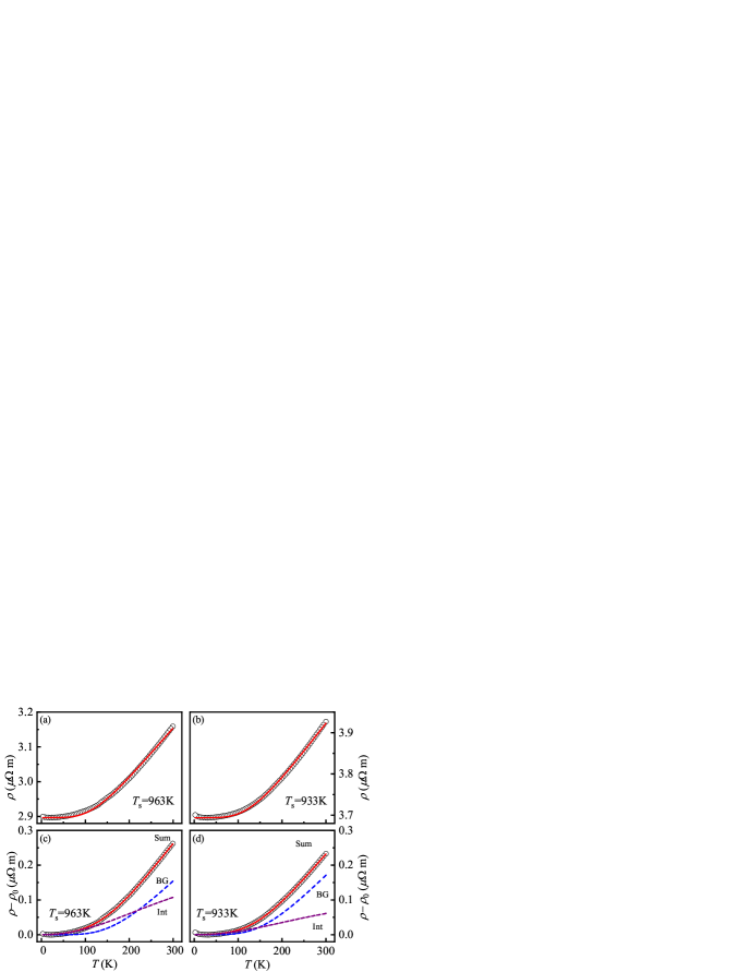
We firstly investigate the electrical transport properties of the Ta:SnO2 films deposited in pure argon. Figures 3(a) and 3(b) show the temperature dependence of resistivity for two representative thick films deposited at and 963 K, respectively. Upon cooling from 300 K, the resistivity decreases with decreasing temperature, and reaches its minimum at (the value of depends on the film and is 30 K and 20 K for the films deposited at and 963 K, respectively), and then slightly increases with further decreasing temperature. The slight enhancement in resistivity with decreasing temperature could originate from weak-localization (WL) effect and electron-electron interaction (EEI) effect. [27] The reduction of resistivity with decreasing temperature above indicates that Ta:SnO2 film reveals degenerate semiconductor characteristics in electrical transport properties. It is also found that the carrier (conduction electron) concentrations of the thick films are insensitive to temperature from room temperature down to liquid helium temperature, which further confirms the degenerate semiconductor characteristics of the films.
Generally, the resistivity for a degenerate semiconductor or metal comes from two effects: the residual resistivity caused by collisions of electrons with impurity atoms and mechanical imperfections in lattice and the temperature-dependent resistivity originated from electron-phonon scattering. According to Altshuler[28, 29, 30], the temperature dependence of resistivity caused by the “pure” electron-phonon scattering in disordered metal is similar to the Bloch-Grüneisen formula. Thus the total resistivity can be written as[31, 32, 33, 34]
| (2) |
where is the residual resistivity, is a constant, and is the Debye temperature. The theoretical predictions of Eq. (2) are least-squares fitted to the data of the Ta:SnO2 films from to 300 K and the results are shown as solid curves in Figs. 3(a) and 3(b). Clearly, the overall trends of the experimental data can be described by Eq. (2). However, a close inspection indicates that the data below 120 K remarkably deviate from the theoretical predictions. Thus other scattering processes could be neglected in above analysis.
Since 1987, Reizer and Sergeev have realized the importance of the inelastic electron scattering from vibrating impurities in dirty metals. [35] In this case, the contribution to the resistivity due to the interference between the electron-phonon and electron-impurity scattering can be expressed as[36, 37, 38]
| (3) |
where is a material-related constant and can be approximately written as . Here is the Bolzmann constant, is Fermi energy, is the Fermi momentum, and and are the sound speed of longitudinal and transverse phonons. For , the integral in the right hand side of Eq. (3) tends to , then Eq. (3) is simplified as . Considering the contribution of interference mechanism, one can obtain
| (4) |
where is the resistivity caused by “pure” electron-phonon scattering and is represented by the second term in the right hand side of Eq. (2). The theoretical predictions of Eq. (4) are least-squares fitted to the experimental data in Figs. 3(a) and 3(b), and the results are redrawn in Fig. 3(c) and 3(d), respectively, for clarity. The optimal parameters obtained from the fitting processes are listed in Table 1. In Fig. 3(c) and 3(d), we also give the temperature dependence of and for each film. Clearly, the interference mechanism dominates over the “pure” electron-phonon scattering term at low temperature regime (the exact value of the up bound temperature below which is less than is sample dependent). These results indicate that the effect of interference between the electron-phonon and electron-impurity scattering plays a key role in the low-temperature electrical transport processes of Ta:SnO2 films. We note in passing that the electron-phonon-impurity interference effect can be neglected in the films deposited at K and . The reason needs further investigations.
III.3 Intergrain electron-electron interaction effect on the transport in the thin films
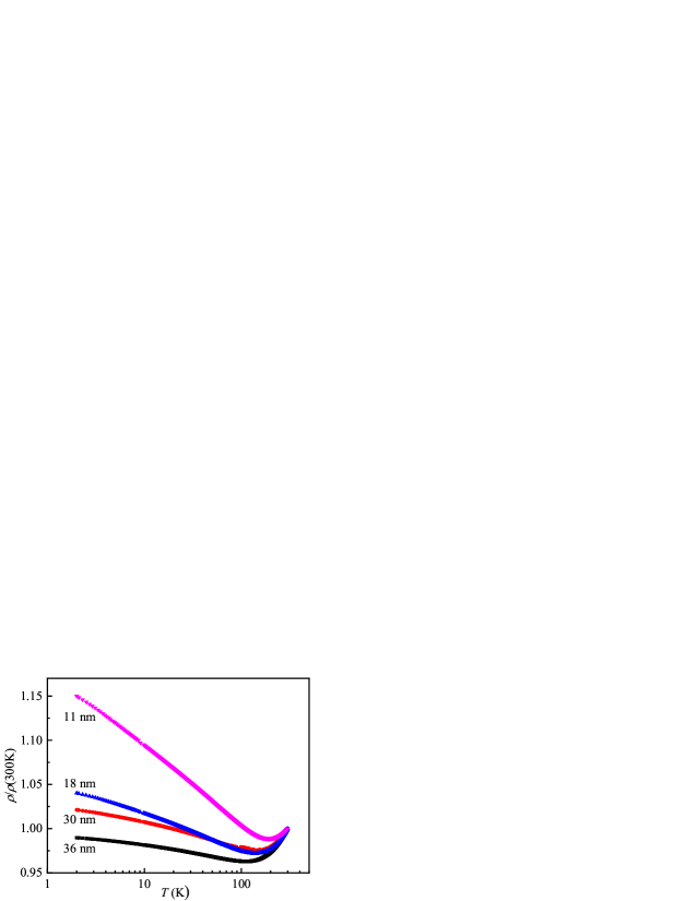
Now we discuss the longitudinal and Hall transport properties of Ta:SnO2 films with thickness ranging from 11 to 36 nm. Figure 4 shows the temperature dependence of resistivity of these thin films deposited at K and . Although the overall variation trends of curves for these films are similar to those of the thick Ta:SiO2 films, the enhancement of resistivity with decreasing temperature below is more remarkable than that in those thick films. In addition, the resistivity approximately varies linearly with (or ) below . This indicates that the increasing in resistivity with decreasing temperature in the low temperature regime could originate from corrections of WL and EEI effects in two-dimensional (2D) disordered conductors. [39]
The WL and EEI effects in homogeneous disordered metals have been intensively investigated since 1980s. [39, 40, 41, 42] In 2D homogeneous disordered metals, the Altshuler-Aronov type EEI effect gives the follow correction to the conductivity[39, 40]
| (5) |
where is an electron screening factor and is the elastic scattering time. When a magnetic field is applied, the correction can be expressed as[43, 27, 44, 45]
| (6) |
where with being the Landé g-factor, the function can be computed numerically and has the value and for and , respectively. [43]
Since 2002, it has been realized that the EEI effect in granular metals is distinct from that in “homogeneous disordered metals”. [47, 48, 49, 50, 51, 52] The term granular metals refers to composite materials consisting of immiscible metals and insulators. In granular metals, the intergrain electron and intragrain dynamics both play key roles in the electrical transport properties. In strong intergrain coupling regime, [i.e., , where , , and are intergrain tunneling conductance and conductance of a metal grain, respectively], the EEI effect in the presence of granularity gives distinct corrections to both logarithmic conductivity and Hall coefficient. According to the theory, in the temperature range ( is the mean-energy level spacing in the grain and is the charging energy), the conductivity is determined by the granular structure and incoherent tunneling processes, and can be written as[47, 48, 49, 50]
| (7) |
where is the conductivity without the EEI effect and is the dimensionality of the granular array. In the temperature range , the virtual electron diffusion inside individual grains governs the temperature dependent behavior of the Hall coefficient[51, 52]
| (8) |
where is the effective carrier concentration, is a numerical lattice factor of order unity, is the Thouless energy. It should be noted that the dependent behaviors of in Eq. (7) and in Eq. (8) are independent of the granular array dimensionality, and are the consequence of and specific to the granularity.
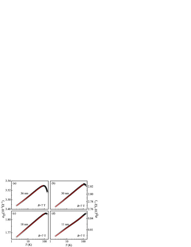
To understand which kind of EEI effect governs the low temperature transport properties of these thin films, we measured the temperature dependence of conductivity of the films in a perpendicular magnetic field of 7 T, which is sufficiently large to suppress the WL effect. [46] Figure 5 shows the sheet conductivity as a function of logarithm of temperature, where is the reciprocal of the sheet resistance. Clearly, the sheet conductivity varies linearly with , or from 2 to 90 K. We firstly compare the data with Eq. (6). At low temperature and large magnetic field, Eq. (6) can be rewritten as
| (9) |
where is an arbitrary reference temperature. Taking K, we fit the data to Eq. (9)using least-square method. Although the experimental data overlap with the theoretical predictions of Eq. (5), the fitted values of are all negative, e.g. , , , and for the , 30, 18, and 11 nm films, respectively. Theoretically, the value of the screening factor should be . Thus the negative value of indicates that the behavior of does not originate from the Altshuler-Aronov type EEI effect.
Next we analyze the data in the framework of the EEI theory in the presence of granularity. From Table 1, one can see that the mean grain sizes of the , 30, 18, and 11 nm films are 31.6, 24.2, 17.7 and 9.8 nm, respectively, thus these films are nominally covered with only one layer of Ta:SnO2 grains and the dimensionality of the grain array is for each film. For 2D granular system, we rewrite Eq. (7) as
| (10) |
where is the sheet conductance [corresponding to the in Eq. (7)] without the EEI effect. Treating as an adjusting parameter, we fit the data to Eq. (10) by taking K and and the results are plotted as solid lines in Fig. 5. Inspection of Fig. 5 indicates that the data for the four films can be well described by Eq. (10). In addition, the fitted values of the adjustable parameter all satisfy, (see Table 1), the prerequisite for the validation of Eq. (10).
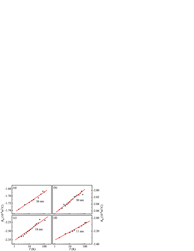
Figure 6 shows the Hall coefficient varies as a function of temperature for the four thin films, where the temperature axis is plotted in logarithmic scale. Clearly, the Hall coefficients vary linearly with . Similarly, Eq. (8) is rewritten as
| (11) |
Our measured data are least-squares fitted to Eq. (11) and the fitted results are represented by the solid lines in Fig. 6. In the fitting processes, is the adjustable parameter, has been obtained in fitting the data, is set as 2 K, and is taken the mean value measured between 180 and 250 K, in which the EEI correction to can be neglected. The values of and for each film are listed in Table 1. Clearly, the data of these thin films are overlapped with the theoretical prediction of Eq. (8). The values of are in the reasonable range. Thus Eqs. (10) and (11) are safely applicable for the thin films.
Before closing this subsection, we summarize the experimental advances in the study of the influence of Coulomb effects on the transport properties in granular metals. Soon after the theoretical finding of the law [Eq. (7)], it was tested in several granular systems, including Pt/C composite nanwires, [53, 54] B-doped diamond films, [55] and granular Cr films. [56] Thus the law was verified. To verify law [Eq. (8)], one generally needs to measure the Hall voltage versus magnetic field at each testing temperature. This is much more difficult than the conductivity versus temperature measurement (the logarithmic correction term is estimated to be less than 10% of the total ). Taking advantage of the low carrier concentration and degenerate semiconductor characteristics of tin-doped indium oxide (ITO) films, Zhang et al. [57] verified Eq. (8) as well as Eq. (7) in 2D ITO granular films. Shortly afterwards, Yang et al. [58] also demonstrated the validity of Eq. (8) and Eq. (7) in 2D Al-doped ZnO granular arrays. In 2015, Wu et al. measured the temperature dependence of conductivities and Hall coefficients of in 2D and 3D Agx(SnO2)1-x ( being the volume fraction of Ag) granular composites. [59] They observed a law as well as a law in a wide temperature range. These temperature behaviors are independent of the dimensionality of granular arrays, and can be explained by the EEI effects in the presence of granularity. In the thin Ta:SnO2 films (this paper), each grain is treated as a metallic particle () and the carrier concentration in each film is 2 to 3 orders of magnitude lower than those in typical metals (which facilitates the measurement of the temperature dependence of ). The experimental [] data are least-square fitted to Eq. (10) [Eq. (11)] instead of Eq. (7) [Eq. (8)]. This ensures only one parameter [ in Eq. (10) or in Eq. (11)] can be adjusted in the fitting process. Thus the uncertainty arisen in estimating or is avoided. In fact, the value of or is difficult to be estimated in 2D granular arrays with disk-shaped granules.[56, 57, 58] Overall, our results in the thin Ta:SnO2 films further confirm that the EEI effects on the transport properties in granular metals are different from that in homogeneous disordered metals.
IV Conclusion
In summary, Ta:SnO2 films with low resistivity and high optical transparency are successfully fabricated by rf-sputtering methods. It is found that the optimal depositing conditions for low resistivity and high optical transparency are K and . The electrical transport properties of the thick films and thin films are systematically investigated. It is found that all films have degenerate semiconductor characteristics. For the thick films deposited at pure argon, besides the electron-phonon scattering, the interference effect between electron-phonon and electron-impurity scattering also plays an important role in determining the temperature dependent behaviors of the resistivity. For the thin films, the robust law and law have been observed from liquid helium temperature to 100 K. We have found that the behaviors of the conductivity and Hall coefficient originate from the EEI effect in the presence of granularity. Our results show that the Ta:SnO2 film, although a new TCO material, can be a model system for exploration new electrical transport phenomena.
Acknowledgements.
This work is supported by the National Natural Science Foundation of China through Grant No. 11774253 and 12174282.DATA AVAILABILITY
The data that support the findings of this study are available from the corresponding author upon reasonable request.
References
- [1] Z. M. Jarzebski, Phys. Stat. Sol. 71, 13 (1982).
- [2] G. J. Exarhos and X. D. Zhou, Thin Solid Films 515, 7025 (2007).
- [3] S. G. David and D. Clark, MRS. Bulletin. 25, 15 (2010).
- [4] E. Gilshtein, S. Bolat, G. T. Sevilla, A. C. Vidani, Clemens, T. Graule, A. N. Tiwari, and Y. E. Romanyuk, Adv. Mater. Technol. 5, 2000369 (2020).
- [5] A. K. Singh, A. Janotti, M. Scheffler, and C. G. V. Walle, Phys. Rev. Lett. 101, 055502 (2008).
- [6] H. Kim, G. P. Kushto, R. C. Y. Auyeung, and A. Piqué, Appl. Phys. A 93, 521 (2008).
- [7] Z. Hu, J. Zhang, Z. Hao, Q. Hao, X. Geng, and Y. Zhao, Appl. Phys. Lett. 98, 123302 (2011).
- [8] R. G. Gordon, MRS. Bulletin. 25, 52 (2000).
- [9] P. D. C. King and T. D. Veal, J. Phys.: Conden. Matter 23, 334214 (2011).
- [10] B. H. Gao, S. N. Ding, Q. Q. Li, D. S. Shan, M. Yue, and S. Cosnier, Electroanal. 24, 1267 (2012).
- [11] M. A. Islam, J. R. Mou, M. F. Hossain, A. M. M. T. Karim, M. Kamruzzaman, and M. S. Hossain, J. Solgel Sci. Technol. 96, 304 (2020).
- [12] A. E. Rakhshani, Y. Makdisi, and H. A. Ramazaniyan, J. Appl. Phys. 83, 1049 (1998).
- [13] X. L. Shi, J. T. Wang, and J. N. Wang, J. Alloys Compd. 611, 297 (2014).
- [14] S. Suh, Z. H. Zhang, W. K. Chu, and M. H. David, Thin Solid Films 345, 240 (1999).
- [15] S. Y. Lee and B. O. Park, Thin Solid Films 510, 154 (2006).
- [16] C. Y. Kim, E. B. Go, J. S. Choi, and S. C. Choi, J. Nanosci. Nanotechnol. 16, 11330 (2016).
- [17] G. Jain and R. Kumar, Opt. Mater. 26, 27 (2004).
- [18] H. Kim, R. C. Y. Auyeung, and A. Piqué, Thin Solid Films 516, 5052 (2008).
- [19] A. Schleife and F. Bechstedt, J. Mater. Res. 27, 2180 (2012).
- [20] Germán N. Darriba, Emiliano L. Muñoz, Leonardo A. Errico, and Mario. Rentería, J. Phys. Chem. C. 118, 19929 (2014).
- [21] M. Behtash, P. H. Joo, S. Nazir, and K. S. Yang, J. Appl. Phys. 117, 175101 (2015).
- [22] L. S. Birks and H. Friedman, J. Appl. Phys. 17, 687 (1946).
- [23] K. Ishikawa, K. Yoshikawa, and N. Okada, Phys. Rev. B 37, 5852 (1988).
- [24] X.C. Yang, W. Riehemann, M. Dubiel, and H. Hofmeister, Mater. Sci. Eng. B 95, 299 (2002).
- [25] C.R. Mariappan, C. Galven, M.P. Crosnier-Lopez, F. Le Berre, and O. Bohnke, J. Solid State Chem. 179, 450 (2006).
- [26] J. Tauc, R. Grigorovici, and A. Vancu, Phys. Status Solidi 15, 627 (1966).
- [27] P. A. Lee and T. V. Ramakrishnan, Rev. Mod. Phys. 57, 287 (1985).
- [28] B. L. Altshuler, Zh Eksp. Teor. Fiz. 75, 1330 (1978) [Sov. Phys. JEPT 48, 670 (1978)].
- [29] B. L. Altshuler, A. G. Aronov, and D. E. Khmelnitsky, J. Phys. C: Solid State 15, 7367 (1982).
- [30] B. L. Altshuler and A. G. Aronov, in Electron-Electron Interactions in Disordered Systems, edited by A. L. Efros and M. Pollak (Elsevier, Amsterdam, 1985).
- [31] J. M. Ziman, Electron and Phonons (Clarendon Press, Oxford, 1960).
- [32] G. Grimvall, The Electron-Phoneon Interaction in Metal (North-Holland, Amsterdam, 1981).
- [33] N. G. Ptitsina, G. M. Chulkova, K. S. Il’in, A. V. Sergeev, F. S. Pochinkov, E. M. Gershenzon, and M. E. Gershenson, Phys. Rev. B 56, 10089 (1997).
- [34] Z. Q. Li and J. J. Lin, J. Appl. Phys. 96, 5918 (2004)
- [35] M. Yu. Reizer and A. V. Sergeev, Zh. Eksp. Teor. Fiz. 92, 2291 (1987) [Sov. Phys. JETP 65, 1291 (1987)].
- [36] P. M. Echternach, M. E. Gershenson, and H. M. Bozler, Phys. Rev. B 47, 13659 (1993).
- [37] S. S. Yeh, J. J. Lin, X. N. Jing, and D. L. Zhang, Phys. Rev. B 72, 024204 (2005).
- [38] K. S. Il’in, N. G. Ptitsina, A. V. Sergeev, G. N. Gol’tsman, E. M. Gershenzon, B. S. Karasik, and E. V. Pechen, Phys. Rev. B 57, 15623 (1998).
- [39] B. L. Altshuler, D. Khmel’nitzkii, A. I. Larkin, and P. A. Lee, Phys. Rev. B 22, 5142 (1980).
- [40] B. L. Altshuler, A. G. Aronov, and P. A. Lee, Phys. Rev. Lett. 44, 1288 (1980).
- [41] Y. M. Blanter and A. D. Mirlin, Phys. Rev. B 57, 4566 (1998).
- [42] K. E. J. Goh, M. Y. Simmons, and A. R. Hamilton, Phys. Rev. B 77, 235410 (2008).
- [43] P. A. Lee and T. V. Ramakrishnan, Phys. Rev. B 26, 4009 (1982).
- [44] A. G. Mal’shukov, K. A. Chao, and M. Willander, Phys. Rev. B 56, 6436 (1997).
- [45] G. Bergmann, Int. J. Mod. Phys. B 24, 2015 (2010).
- [46] The characteristic dephasing field for WL with being the dephasing length. is appromately equal to 3.0 T at 80 K for the nm Ta:SnO2 films, and decreases with decreasing temperature. At a certain temperature, the values of for other thin films are less than that for the 11 nm thick film.
- [47] K. B. Efetov and A. Tschersich, Europhys. Lett. 59, 114 (2002).
- [48] I. S. Beloborodov, K. B. Efetov, A. V. Lopatin, and V. M. Vinokur, Phys. Rev. Lett. 91, 246801 (2003).
- [49] K. B. Efetov and A. Tschersich, Phys. Rev. B 67, 174205 (2003).
- [50] I. S. Beloborodov, A. V. Lopatin, V. M. Vinokur, and K. B. Efetov, Rev. Mod. Phys. 79, 469 (2007).
- [51] M. Y. Kharitonov and K. B. Efetov, Phys. Rev. Lett. 99, 056803 (2007).
- [52] M. Y. Kharitonov and K. B. Efetov, Phys. Rev. B 77, 045116 (2008).
- [53] L. Rotkina, S. Oh, J. N. Eckstein, and S. V. Rotkin, Phys. Rev. B 72, 233407 (2005).
- [54] R. Sachser, F. Porrati, C. H. Schwalb, and M. Huth, Phys. Rev. Lett. 107, 206803 (2011).
- [55] P. Achatz, W. Gajewski, E. Bustarret, C. Marcenat, R. Piquerel, C. Chapelier, T. Dubouchet, O. A. Williams, K. Haenen, J. A. Garrido, and M. Stutzmann, Phys. Rev. B 79, 201203(R) (2009).
- [56] Y. C. Sun, S. S. Yeh, and J. J. Lin, Phys. Rev. B 82, 054203 (2010).
- [57] Y. J. Zhang, Z. Q. Li, and J. J. Lin, Phys. Rev. B 84, 052202 (2011).
- [58] Y. Yang, Y. J. Zhang, X. D. Liu, and Z. Q. Li, Appl. Phys. Lett. 100, 262101 (2012).
- [59] Y. N.Wu, Y. F. Wei, Z. Q. Li, and J. J. Lin, Phys. Rev. B 91, 104201 (2015).