3D Fermi surfaces from charge order in layered CsV3Sb5
Abstract
The cascade of electronic phases in CsV3Sb5 raises the prospect to disentangle their mutual interactions in a clean, strongly interacting Kagome lattice. When the Kagome planes are stacked into a crystal, its electronic dimensionality encodes how much of the Kagome physics and its topological aspects survive. The layered structure of CsV3Sb5 reflects in Brillouin-zone-sized quasi-2D Fermi surfaces and a significant transport anisotropy. Yet here we demonstrate that CsV3Sb5 is a three-dimensional metal within the charge-density-wave (CDW) state. Small 3D pockets play a crucial role in its low-temperature magneto- and quantum transport. Their emergence at results in an anomalous sudden increase of the in-plane magnetoresistance by 4 orders of magnitude. The presence of these 3D pockets is further confirmed by quantum oscillations under in-plane magnetic fields - demonstrating their closed nature. These results emphasize the impact of interlayer coupling on the Kagome physics in 3D materials.
introduction
When structurally layered materials host strong electronic correlations, their effective electronic dimensionality is key to understanding their microscopic physics. The anisotropic Fermi surface then sets the canvas on which correlated ground states unfold, such as magnetism, charge-density-waves (CDW) or superconductivity. Cuprate and pnictide high-temperature superconductors are prime examples of layered materials in which reduced dimensionality defines the superconducting stateBednorz and Müller (1986); Kamihara et al. (2006). The anisotropy is further a critical parameter to describe the vortex formation and the orbital limit of the upper critical field. Recently, metals hosting planes with Kagome nets have attracted significant attention due to their topological phases as well as potential correlation effectsKida et al. (2011); Kang et al. (2020); Ortiz et al. (2019). The latter have been argued to arise from small-bandwidth bands (flat bands) that are predicted in phenotypical two-dimensional Kagome modelsO’Brien et al. (2010). Flat bands naturally enhance correlation effects when the Coulomb energy exceeds the kinetic energy and they lead to a divergent density of states, an entropic catastrophe which is commonly avoided by the formation of electronically ordered states at low temperatures. However when the Kagome nets are stacked into a three-dimensional crystal, the existence of flat bands depends on the strength of the interlayer hybridization and its impact on the band dispersion. Therefore in order to explore how much Kagome physics survives in a 3D metal, it is necessary to investigate the electronic structure and especially its effective dimensionality.
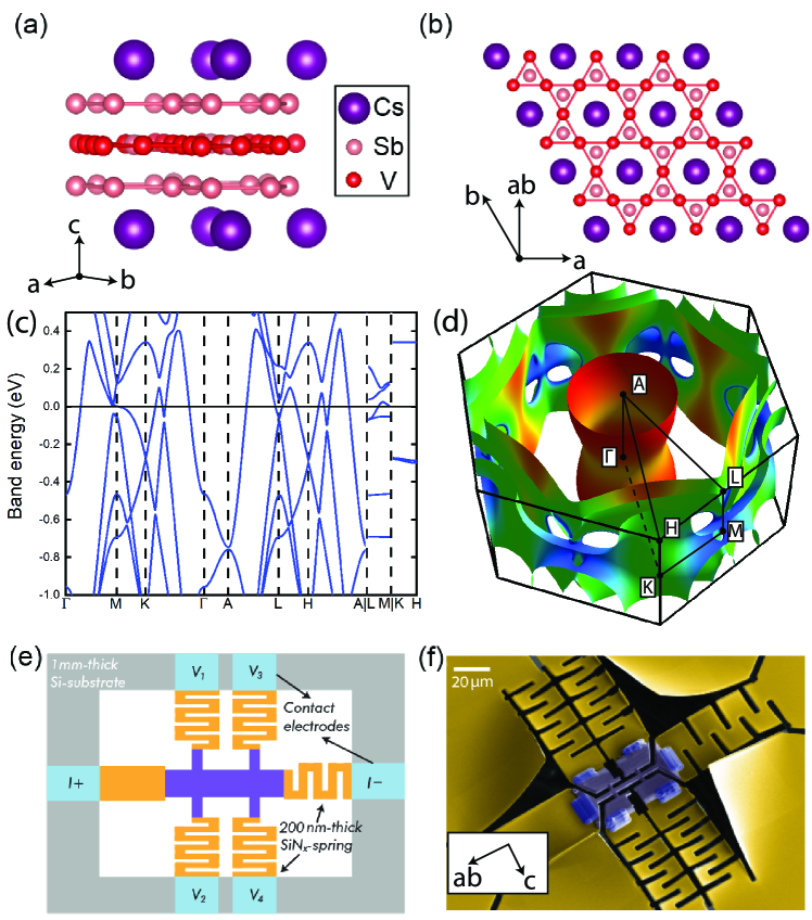
Here we investigate the electronic dimensionality of CsV3Sb5 [Fig. 1(a) and (b)], a stacked Kagome crystal, and its influence on the rich physics it hosts such as the non-trivial band topology, superconductivity and CDW order. The non-magnetic Kagome nets formed by Vanadium atoms result in a symmetry-enforced pair of topological bands with opposite Chern numbers Ortiz et al. (2019, 2020); Fu et al. (2021); Chen et al. (2022). The hybridization with Sb atoms effectively expands the band width and therefore the flat band gains sizable dispersion yet it leaves multiple bulk Dirac points intact, as observed by angle-resolved photoemission spectroscopy (ARPES)Ortiz et al. (2020); Luo et al. (2021). Upon cooling, the Kagome lattice undergoes a CDW transition at = 93 K Yu et al. (2021a); Mu et al. (2021); Liang et al. (2021). The 22 reconstruction within the Kagome plane is accompanied by a phase shift of the CDW across an atomic step edge as observed by STM experiments Zhao et al. (2021); Liang et al. (2021), suggesting a band reconstruction along the -direction. X-ray studies further suggest a 224 superlattice formation Wu et al. (2022); Stahl et al. (2022) with long range out-of-plane coherence, again highlighting the importance of out-of-plane coupling in this system. At even lower temperatures of K, superconductivity appearsOrtiz et al. (2020). The large upper critical field anisotropy ( 9) is a result of its anisotropic superconducting propertiesNi et al. (2021). Meanwhile the non-trivial band topology may give rise to topological superconductivity. Indeed, STM has uncovered a zero-bias peak in the vortex cores which, while not conclusive, is compatible with a scenario of bound Majorana statesLiang et al. (2021).
Results
The single-particle band structure from ab-initio calculations serves as a starting point to investigate the dimensionality of this strongly correlated compound. The electronic structure of CsV3Sb5 in the high-symmetry state at room temperature is calculated using density functional theory (DFT) methods, the computational details can be found in the Supplementary materialsGiannozzi et al. (2017); Perdew et al. (1996); Dal Corso (2014); Methfessel and Paxton (1989); Mostofi et al. . Multiple bands are found at the Fermi level [Fig. 1(c)], consistent with the previous reportsOrtiz et al. (2019, 2020); Fu et al. (2021). Accordingly, multiple Fermi surfaces of cylindrical shape are expected in the Brillouin zone [Fig. 1(d)]. While the layered structure is reflected in the electron-like cylinders centered at and K, their sizable dispersion signals pronounced interlayer coupling. In absence of spin-orbit coupling (SOC), the cylinder at the Brillouin zone boundary (H to K) would surround a nodal line, yet SOC breaks this degeneracy gapping the nodal line.
The band structure of CsV3Sb5 indicates a clear out-of-plane dispersion, giving rise to warping of the cylindrical Fermi surfaces. Experimentally the electronic dimensionality can be explored via the resistivity anisotropy. As common in structurally layered materials, CsV3Sb5 crystals grow as thin platelets along the Kagome plane Ortiz et al. (2019). While this crystal morphology lends itself to in-plane resistivity measurements, quantitative out-of-plane transport poses a well-known challenge. Focused Ion Beam (FIB) milling can be used to prepare micron-sized -direction bars with well-defined geometries to quantify the resistivityMoll (2018). CsV3Sb5 like other soft CDW-compounds is susceptible to mechanical strainSong et al. (2021); Du et al. (2021), we suspend the microstructured sample (purple) in free space. It is mechanically and electrically connected to a supportive silicon frame only via thin, gold-coated SiNx membrane microsprings (gold) [Fig. 1(e) and (f)]. These structures exert only minimal residual pressure on the sample ( 9.8 bar, see supplement), thus allowing an intrinsic evolution of the ordered states. Moreover, a low-voltage polish step at 5 kV reduces the amorphization layer into the nm-rangeKelley et al. (2013) which minimizes its possible influence.
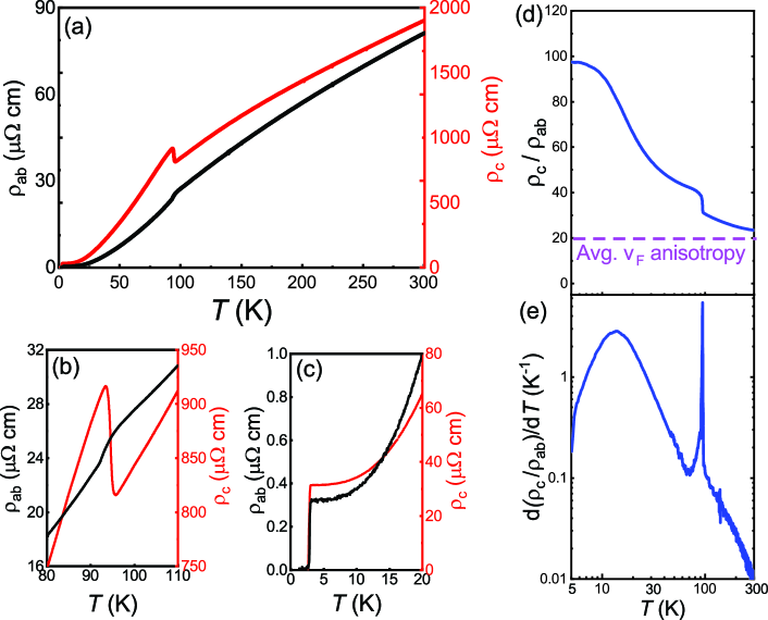
In these suspended structures, the in-plane resistivity decreases from 80 cm at 300 K to 0.3 cm at K. The high residual resistivity ratio (RRR) of 250 is comparable to bulk samplesChen et al. (2022), evidencing the high quality of the microstructure fabrication (Fig. 2). The in-plane resistivity displays a small yet sharply defined discontinuity at the CDW transition at which is consistent with previous reportsChen et al. (2022); Ortiz et al. (2019); Xiang et al. (2021). The out-of-plane resistivity, , is comparably larger yet shows an overall similar metallic temperature dependence. It decreases from (300K) 1.9 mcm to () 33 cm, corresponding to a lower RRR of 60. These results are qualitatively reflected in the challenging measurements of on bulk crystals Ortiz et al. (2020); Xiang et al. (2021), yet deviate quantitatively. In comparison to the in-plane resistivity, shows an upwards jump at [Fig. 2(c)]. This jump is much more pronounced compared to the change of for in-plane resistivity. This relative difference again emphasizes the importance of the CDW in the out-of-plane direction.
Further information about the electronic dimensionality is contained in the temperature dependence of the anisotropy. At high temperatures above , the picture of an anisotropic metal emerges [], which falls close to the Fermi velocity anisotropy when averaged over the entire Fermi surface (, [Fig. 2(d)]). The dominant carrier density originates from the Brillouin-zone-sized hexagonal Fermi surfaces with weak dispersion. These feature six almost flat surfaces parallel to the crystalline -directions [Fig. 1(b)], which play an important role in the magneto-transport as discussed later.
Further lowering the temperature beyond the jump at increases the anisotropy which eventually saturates around 100 at , suggesting dominant in-plane electronic transport at low temperatures. Yet reaches a low value of 33 at , which signals metallic three-dimensional transport. The first-order derivative of the resistivity anisotropy reveals further, more subtle changes in the material [Fig. 2(e)]. Besides the clear spike at , a local minimum occurs at around 70 K. This temperature coincides with the onset of anisotropy in the muon spin depolarization rate that has been associated with time-reversal-symmetry breaking (TRSB)Yu et al. (2021b). The TRSB state has been theoretically proposed to arise from an effective orbital current loop fluxDenner et al. (2021); Feng et al. (2021), and a modification of a magnetic scattering channel would be a natural connection between this experiment and ours.
This further emphasizes the emerging question about its effective electronic dimensionality. The large resistivity anisotropy is compatible with an effective 2D description, which may be captured by a simplified model based on a 2D Kagome lattice. Yet to discuss the effective dimensionality, one has to carefully distinguish between the transport dimensionality and the dimensionality of the Fermi surface. In general, the transport anisotropy is determined by the Fermi velocity and the scattering time distribution while the Fermi surface topology encodes another aspect of electronic dimensionality. For example, a cylindrical Fermi surface with strong warping naturally features low transport anisotropy. Here we demonstrate that CsV3Sb5 is a 3D Kagome metal as the emergent small, closed Fermi pockets play a crucial role in its magneto- and quantum transport properties.
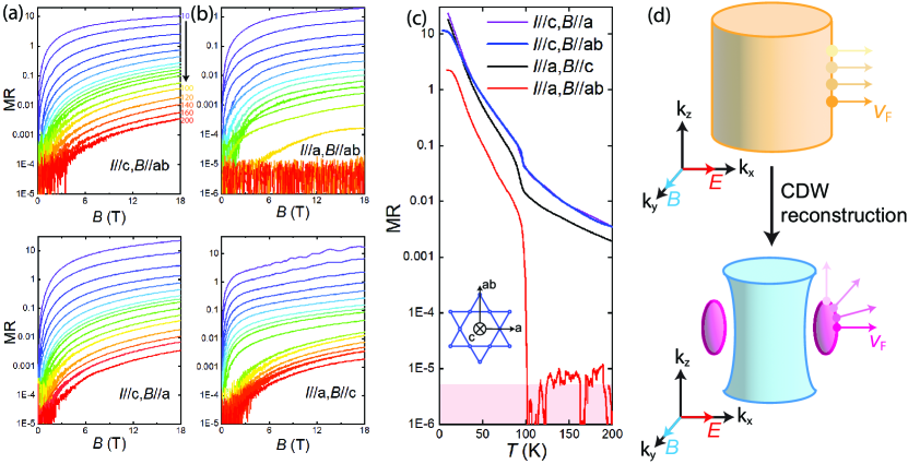
The magnetoresistance provides further information about the electronic dimensionality (Fig. 3). Most intriguing is the complete absence of transverse magnetoresistance for orthogonal in-plane fields and currents at any temperature above . The field-independent noise floor provides an upper bound for the magnetoresistance, at ((18 T)-(0 T))/(0 T) 10-5 at 120 K. Even rather unsuspicious metals such as Cu commonly show transverse magnetoresistance around (20T) at room temperature and (20T) at 100KDe Launay et al. (1959). In contrast, for all other orthogonal current and field orientations in CsV3Sb5, the magnetoresistance increases with decreasing temperature following a conventional semiclassical scaling of the magneto-transport by . Given the complex Fermi surface and putative incipient TRSB order, such absent magnetoresistance for one particular direction appears quite exotic.
The reconstruction of the main cylindrical Fermi surfaces at offers a natural explanation for such behavior. When a current is applied in the plane, the conductivity is dominated by the weakly warped main Fermi surfaces [Fig. 3(d)]. Such flatness ensures that the quasiparticle velocity remains approximately unchanged by the Lorentz force. This behavior is commonly observed in quasi-2D materials when only cylindrical Fermi surfaces are presentKorin-Hamzić et al. (2002); Wosnitza (2006). For magnetic field or current applied along any other direction, magnetoresistance is bound to appear as the Lorentz force significantly impacts the carrier trajectories. These results consistently demonstrate that CsV3Sb5 is electronically quasi-2D above .
However, this conclusion no longer holds in the charge ordered phase. Though the exact type of CDW reconstruction is still under debate, all different scenarios predict the emergence of small closed 3D pockets as a direct consequence of zone foldingOrtiz et al. (2021). Compared to the quasi-2D Fermi surfaces, these small pockets support closed cyclotron orbits which leads to the sudden recovery of magnetoresistance [Fig. 3(d)]. The direct connection between the abrupt change of magnetoresistance and Fermi surface reconstruction further demonstrates the importance of the small, closed pockets to the 3D electronic transport properties of CsV3Sb5, especially at low temperatures.
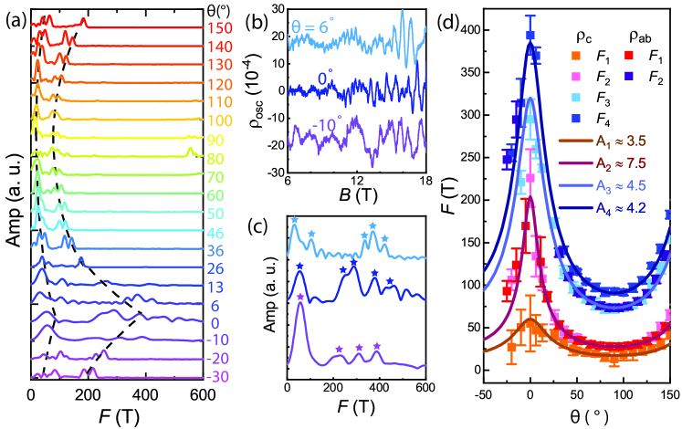
Such small, 3D-like pockets at low temperature should be visible in quantum oscillations. Four low frequency quantum oscillations have been reported for out-of-plane fields and associated with these small 3D pocketsOrtiz et al. (2021); Yu et al. (2021a). However, these quantum oscillations were observed to quickly disappear as the field is rotated towards the plane, which precluded the distinction between a closed, 3D pocket and an open, 2D cylinder. The weakly perturbed, suspended microbars now allow to track this frequency over the entire angle range, firmly establishing them as closed 3D pockets within the density wave phase (Fig. 4). At low angles, the oscillation frequencies observed in our structures are consistent with these previous reports. A likely scenario for the loss of amplitude in conventional experiments involves stacking disorder along -direction due to residual strain, which reduces the quantum-coherent transport along the out-of-plane direction. This is consistent with the larger RRR and lower resistivity observed in the microstructures compared to macroscopic crystalsOrtiz et al. (2020); Xiang et al. (2021). The angular dependence of the oscillation frequencies is well described by a simple ellipsoidal model . The factor characterizes the anisotropy of the i-th Fermi surface [Fig. 4(d)]. These results further support the presence of 3D pockets as suggested by the unusual magneto-transport. The emergence of 3D Fermi pockets due to CDW reconstruction has already been observed in other CDW materials Knowles et al. (2020); Tam et al. (2022) as a 3D zone-folding of Brillouin-zone-sized Fermi surface naturally results in small Fermi surface pockets. These pockets are connected by the 3/4 Bragg wavevector in the 3Q directions which results in an exotic pairing density wave phase at low temperatureZhou and Wang (2021), as observed in STM experiments Chen et al. (2021).
In conclusion, the electronic anisotropy and Fermiology of charge-ordered CsV3Sb5 are characterized by the coexistence of a high-mobility in-plane electronic system with small 3D pockets. They emerge when the charge order is established, demonstrating an electronic dimensionality crossover at . Therefore the interlayer coupling must be taken into account for theoretical modelling as considerations based on 2D Kagome lattices may miss important aspects of this material. It will be highly interesting to explore how the cascades of correlated electronic states are influenced by the coupling between Kagome nets.
References
References
- Bednorz and Müller (1986) J. G. Bednorz and K. A. Müller, Z. Phys. B Condens. 64, 189 (1986).
- Kamihara et al. (2006) Y. Kamihara, H. Hiramatsu, M. Hirano, R. Kawamura, H. Yanagi, T. Kamiya, and H. Hosono, J. Am. Chem. Soc. 128, 10012 (2006).
- Kida et al. (2011) T. Kida, L. Fenner, A. Dee, I. Terasaki, M. Hagiwara, and A. Wills, J. Condens. Mat. Phys. 23, 112205 (2011).
- Kang et al. (2020) M. Kang, S. Fang, L. Ye, H. C. Po, J. Denlinger, C. Jozwiak, A. Bostwick, E. Rotenberg, E. Kaxiras, J. G. Checkelsky, et al., Nat. Commun. 11, 4004 (2020).
- Ortiz et al. (2019) B. R. Ortiz, L. C. Gomes, J. R. Morey, M. Winiarski, M. Bordelon, J. S. Mangum, I. W. Oswald, J. A. Rodriguez-Rivera, J. R. Neilson, S. D. Wilson, et al., Phys. Rev. Mater. 3, 094407 (2019).
- O’Brien et al. (2010) A. O’Brien, F. Pollmann, and P. Fulde, Phys. Rev. B 81, 235115 (2010).
- Ortiz et al. (2020) B. R. Ortiz, S. M. Teicher, Y. Hu, J. L. Zuo, P. M. Sarte, E. C. Schueller, A. M. Abeykoon, M. J. Krogstad, S. Rosenkranz, R. Osborn, et al., Phys. Rev. Lett. 125, 247002 (2020).
- Fu et al. (2021) Y. Fu, N. Zhao, Z. Chen, Q. Yin, Z. Tu, C. Gong, C. Xi, X. Zhu, Y. Sun, K. Liu, and H. Lei, Phys. Rev. Lett. 127, 207002 (2021).
- Chen et al. (2022) D. Chen, B. He, M. Yao, Y. Pan, H. Lin, W. Schnelle, Y. Sun, J. Gooth, L. Taillefer, and C. Felser, Phys. Rev. B 105, L201109 (2022).
- Luo et al. (2021) Y. Luo, S. Peng, S. M. Teicher, L. Huai, Y. Hu, B. R. Ortiz, Z. Wei, J. Shen, Z. Ou, B. Wang, et al., arXiv:2106.01248 (2021).
- Yu et al. (2021a) F. Yu, T. Wu, Z. Wang, B. Lei, W. Zhuo, J. Ying, and X. Chen, Phys. Rev. B 104, L041103 (2021a).
- Mu et al. (2021) C. Mu, Q. Yin, Z. Tu, C. Gong, H. Lei, Z. Li, and J. Luo, Chin. Phys. Lett. 38, 077402 (2021).
- Liang et al. (2021) Z. Liang, X. Hou, F. Zhang, W. Ma, P. Wu, Z. Zhang, F. Yu, J.-J. Ying, K. Jiang, L. Shan, et al., Phys. Rev. X 11, 031026 (2021).
- Zhao et al. (2021) H. Zhao, H. Li, B. R. Ortiz, S. M. Teicher, T. Park, M. Ye, Z. Wang, L. Balents, S. D. Wilson, and I. Zeljkovic, Nature 599, 216 (2021).
- Wu et al. (2022) S. Wu, B. R. Ortiz, H. Tan, S. D. Wilson, B. Yan, T. Birol, and G. Blumberg, Phys. Rev. B 105, 155106 (2022).
- Stahl et al. (2022) Q. Stahl, D. Chen, T. Ritschel, C. Shekhar, E. Sadrollahi, M. C. Rahn, O. Ivashko, M. v. Zimmermann, C. Felser, and J. Geck, Phys. Rev. B 105, 195136 (2022).
- Ni et al. (2021) S. Ni, S. Ma, Y. Zhang, J. Yuan, H. Yang, Z. Lu, N. Wang, J. Sun, Z. Zhao, D. Li, et al., Chin. Phys. Lett. 38, 057403 (2021).
- Giannozzi et al. (2017) P. Giannozzi, O. Andreussi, T. Brumme, O. Bunau, M. B. Nardelli, M. Calandra, R. Car, C. Cavazzoni, D. Ceresoli, M. Cococcioni, N. Colonna, I. Carnimeo, A. D. Corso, S. de Gironcoli, P. Delugas, R. A. D. Jr, A. Ferretti, A. Floris, G. Fratesi, G. Fugallo, R. Gebauer, U. Gerstmann, F. Giustino, T. Gorni, J. Jia, M. Kawamura, H.-Y. Ko, A. Kokalj, E. Küçükbenli, M. Lazzeri, M. Marsili, N. Marzari, F. Mauri, N. L. Nguyen, H.-V. Nguyen, A. O. de-la Roza, L. Paulatto, S. Poncé, D. Rocca, R. Sabatini, B. Santra, M. Schlipf, A. P. Seitsonen, A. Smogunov, I. Timrov, T. Thonhauser, P. Umari, N. Vast, X. Wu, and S. Baroni, J. Phys. Condens. Mat. 29, 465901 (2017).
- Perdew et al. (1996) J. P. Perdew, K. Burke, and M. Ernzerhof, Phys. Rev. Lett. 77, 3865 (1996).
- Dal Corso (2014) A. Dal Corso, Comp. Mat. Sci. 95, 337 (2014).
- Methfessel and Paxton (1989) M. Methfessel and A. T. Paxton, Phys. Rev. B 40, 3616 (1989).
- (22) A. A. Mostofi, J. R. Yates, G. Pizzi, Y.-S. Lee, I. Souza, D. Vanderbilt, and N. Marzari, Computer Physics Communications 185, 2309 (2014).
- Moll (2018) P. J. W. Moll, Annu. Rev. Condens. Mat. Phys. 9, 147 (2018).
- Song et al. (2021) B. Song, X. Kong, W. Xia, Q. Yin, C. Tu, C. Zhao, D. Dai, K. Meng, Z. Tao, Z. Tu, et al., arXiv:2105.09248 (2021).
- Du et al. (2021) F. Du, S. Luo, B. R. Ortiz, Y. Chen, W. Duan, D. Zhang, X. Lu, S. D. Wilson, Y. Song, and H. Yuan, Phys. Rev. B 103, L220504 (2021).
- Kelley et al. (2013) R. Kelley, K. Song, B. Van Leer, D. Wall, and L. Kwakman, Microsc. Microanal. 19, 862 (2013).
- Xiang et al. (2021) Y. Xiang, Q. Li, Y. Li, W. Xie, H. Yang, Z. Wang, Y. Yao, and H.-H. Wen, Nat. Commun. 12, 6727 (2021).
- Yu et al. (2021b) L. Yu, C. Wang, Y. Zhang, M. Sander, S. Ni, Z. Lu, S. Ma, Z. Wang, Z. Zhao, H. Chen, et al., arXiv:2107.10714 (2021b).
- Denner et al. (2021) M. M. Denner, R. Thomale, and T. Neupert, Phys. Rev. Lett. 127, 217601 (2021).
- Feng et al. (2021) X. Feng, K. Jiang, Z. Wang, and J. Hu, Sci. Bull. 66, 1384 (2021).
- De Launay et al. (1959) J. De Launay, R. Dolecek, and R. Webber, J. Phys. Chem. Solids 11, 37 (1959).
- Korin-Hamzić et al. (2002) B. Korin-Hamzić, M. Basletić, and K. Maki, Europhysics Letters (EPL) 59, 298 (2002).
- Wosnitza (2006) J. Wosnitza, Fermi surfaces of low-dimensional organic metals and superconductors, Vol. 134 (Springer, 2006).
- Ortiz et al. (2021) B. R. Ortiz, S. M. Teicher, L. Kautzsch, P. M. Sarte, J. P. Ruff, R. Seshadri, and S. D. Wilson, Phys. Rev. X 11, 041030 (2021).
- Knowles et al. (2020) P. Knowles, B. Yang, T. Muramatsu, O. Moulding, J. Buhot, C. J. Sayers, E. Da Como, and S. Friedemann, Phys. Rev. Lett. 124, 167602 (2020).
- Tam et al. (2022) C. C. Tam, M. Zhu, J. Ayres, K. Kummer, F. Yakhou-Harris, J. R. Cooper, A. Carrington, and S. M. Hayden, Nature Communications 13, 570 (2022).
- Zhou and Wang (2021) S. Zhou and Z. Wang, arXiv:2110.06266 (2021).
- Chen et al. (2021) H. Chen, H. Yang, B. Hu, Z. Zhao, J. Yuan, Y. Xing, G. Qian, Z. Huang, G. Li, Y. Ye, S. Ma, S. Ni, H. Zhang, Q. Yin, C. Gong, Z. Tu, H. Lei, H. Tan, S. Zhou, C. Shen, X. Dong, B. Yan, Z. Wang, and H.-J. Gao, Nature 599, 222 (2021).
Acknowledgements
Funding: This work was funded by the European Research Council (ERC) under the European Union’s Horizon 2020 research and innovation programme (MiTopMat - grant agreement No. 715730). This project received funding by the Swiss National Science Foundation (Grants No. PP00P2_176789). M.G.V., I. E. and M.G.A. acknowledge the Spanish Ministerio de Ciencia e Innovacion (grant PID2019-109905GB-C21). M.G.V. thanks support to Programa Red Guipuzcoana de Ciencia Tecnología e Innovación 2021 No. 2021-CIEN-000070-01 Gipuzkoa Next and the Deutsche Forschungsgemeinschaft (DFG, German Research Foundation) GA 3314/1-1 – FOR 5249 (QUAST). This work has been supported in part by Basque Government grant IT979-16. This work was also supported by the European Research Council Advanced Grant (No. 742068) “TOPMAT”, the Deutsche Forschungsgemeinschaft (Project-ID No. 258499086) “SFB 1143”, and the DFG through the Würzburg-Dresden Cluster of Excellence on Complexity and Topology in Quantum Matter ct.qmat (EXC 2147, Project-ID No. 39085490).
Competing Interests The authors declare that they have no competing financial interests.