A wide swing charge sensitive amplifier for a prototype Si-W EM calorimeter
Abstract
A wide swing charge sensitive amplifier (CSA) has been developed, as a part of a front-end electronics (FEE) readout ASIC, for a prototype silicon tungsten (Si-W) based electromagnetic (EM) calorimeter. The CSA, designed in 0.35 m N-well CMOS technology using 5V MOS transistors, has a wide linear operating range of 2.6 pC w.r.t the input charge with a power dissipation of 2.3 mW. A noise figure (ENC) of 820 e- at 0 pF of detector capacitance with a noise slope of 25 e-/pF has been achieved (when followed by a CR-RC2 filter of 1.2 s peaking time). This design of CSA provides a dynamic range (ratio of maximum detectable signal to noise floor) of 79 dB for the maximum input charge of 2.6 pC when connected to a silicon detector with a capacitance of 40 pF. Using folded cascode architecture-based input stage and low voltage high swing current mirrors as the load, the CSA provides an enlarged output swing when biasing the output node towards one supply rail and utilizing the voltage range towards the opposite rail. The design philosophy works for both polarities of a large input signal. This paper presents the design of CSA with a wide negative output swing for an anticipated input signal of positive polarity in the target application with a known detector biasing scheme.
keywords:
CSA , wide swing FEE , charge preamplifierurl]souravm@barc.gov.in
1 Introduction
The continuous advancement in the field of particle accelerators for the next generation of high energy physics (HEP) experiments [1] puts forward significant challenges of particle identification, separation, and analysis. Advanced HEP detectors like highly granular calorimeters [2, 3, 4] demand high-density readout FEE with a wide dynamic range (about 80 dB) and a precision better than 1% [1]. Hence, the first stage preamplifier design in the readout FEE chain is critical and should satisfy the dynamic range requirements with adequate signal to noise ratio (SNR) in a power-efficient way to enable high-density integration.
As the first stage of FEE, the CSA is preferred primarily because of its low power, low noise configuration and charge gain’s (AQ) insensitivity to a variation of detector capacitance (CD). For Si-W based EM calorimeter, which involves particle shower formation and dissolution, a wide dynamic range (simultaneous detection of maximum energy deposition few pC in the shower maximum layers and detection of MIP particle, i.e. 4 fC for a silicon detector of 300m wafer thickness [5]) CSA is required as the first stage of FEE.
Various design approaches to address these critical requirements are reported in the literature. A switchable gain charge preamplifier is one of them with multiple feedback capacitances to improve the output swing [6]. Here, the gain variation has to be done either through slow peripheral control [7] or through additional gain selection circuitry involving comparator [8]. The latter option may introduce non-linear behaviour in the circuit during switching among the various gain modes. Two separate charge preamplifier channels with charge division/sharing methods using series capacitance is another reported design scheme [9]. However, this method requires one extra channel per detector element, leading to extra power dissipation, additional area consumption, a compromised low signal performance and increasing cost. A combination of switchable gain CSA with ADC+ToT (Time over Threshold) technique is also reported [10] to extend the swing of the FEE. But, this method has faced few challenges like high cross-talk, long dead time, absence of smooth overlap between the ADC and ToT methods when the preamplifier goes from the non-saturation mode to saturation mode [11].
A wide swing CSA can facilitate all these design methods to achieve an even higher linear operating range. This paper thus reports a design technique to enhance the linear operating range of the charge preamplifier itself by optimizing the output dc point close to one supply rail while utilizing the voltage range toward the opposite supply rail as output swing. Section II presents the architecture of the CSA. The analysis for the major design parameters is provided in section III. Section IV describes the design methodology for the CSA. Simulation results and the layout view of the CSA are reported in section V. Section VI presents the test results of the fabricated and packaged CSA as a part of a bigger FEE ASIC. Finally, section VII concludes the paper.
2 Architecture: The CSA
The known detector biasing scheme in the target application for this CSA is shown in Figure 1a, where RL is the detector bias resistance, D represents a P-N junction (diode) detector, and Ccp is the ac coupling capacitor between the detector and the CSA. In this biasing scheme with an N-type silicon PAD detector, the anode (p-type side) and cathode (n-type side) of the detector are connected to the negative HV and ground. As a result, the expected signal polarity at the output of the CSA is negative, and as it involves one polarity inversion, the equivalent signal polarity at the input will be positive, as shown in Figure 1a.
The CSA has been designed in 0.35 m CMOS technology using 5V MOS transistors with a typical Vthn=0.75 V, Vthp=-1.0 V, and kn=100 A/V2, kp=30 A/V2. In this design, the CSA is optimized to have the output dc bias point close to the positive supply rail ( 4 V) and utilize the voltage swing towards the negative supply rail to allow a large negative signal swing. The threshold voltage of the input transistor (M1) puts the limit on the max output dc voltage. A schematic of the proposed CSA is shown in Figure 1b. The architecture of the CSA is based on three sections; a core amplifier stage (M1-9), a feedback network (Cf (an integrating capacitor) and Rf (a decay resistor)), and the biasing network (M10-14).
The core amplifier is designed using a folded cascode based input stage and low voltage high swing current mirror as the load. Folded cascode architecture facilitates high gain and wide bandwidth design with a minimum number of active components with enhanced output swing and ease of frequency compensation. Low voltage high swing current mirror architecture is chosen as the active load to satisfy the broader dynamic range requirement of the CSA. It reduces the voltage headroom requirement from 2Vdsat+Vth of the cascode current mirror to 2Vdsat apart from providing very high output resistance (of the order of gmr) [12]. Assuming a conservative value of average Vdsat also, this architecture improves the output voltage swing to be wide enough into the supply rails ( VDD – 4Vdsat).
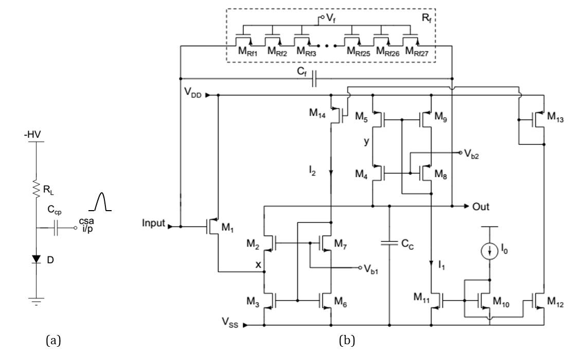
The value of Cf is a trade-off between the charge/conversion gain (AQ) and rise time (shown in A) of the CSA. This work aims to design a wide dynamic range CSA, so Cf was optimized to be 0.8 pF providing a AQ of 1.25 mV/fC (lower AQ leads to enhanced linear range w.r.t. input charge). The dc operating point is set by shunt-shunt feedback using a very high-value Rf (to reduce the thermal noise contribution 4kT/Rf). Rf is implemented by a series of transistors (MRf1-27) operating in the linear/triode region with its gate voltage (Vf) externally controlled to have a variable Rf (2 - 120 MΩ) and adjustable fall time. Series connection of multiple transistors ensures low distortion and improved linearity over a large signal swing. In this design, Vf is externally adjusted for an equivalent feedback resistance of 75 MΩ providing a fall time constant of 60 s for the CSA output response, which again sets a limit in rate capability to 10 kHz.
The biasing network, consisting of transistor M10-14, distributes the required current (I1 and I2) from a master current source (I0) through current mirroring action. Vb1 and Vb2 are optimized bias voltages for maximum swing. Cc is the compensating capacitor at the high impedance output node of the CSA to improve the stability response.
3 Design analysis
In this section, the analysis of the major design parameters (noise and ac performance) of the CSA is performed.
3.1 Noise optimization
The primary noise contributors in a typical detector and front-end readout configuration (as shown in Figure 7 in A) are the shot noise due to the detector leakage current and the electronic noise of the CSA. The expression for effective electronic noise at the input of the core amplifier (considering only the thermal noise contribution of the transistors) of Figure 1b is
| (1) |
Where gm’s are the trans-conductance of the respective transistors, k is the Boltzmann constant, and T is the temperature in Kelvin. By ensuring higher gm1, the effective input noise will be dominated by M1. Then, the total input-referred noise spectral density (including the 1/F noise) of the core amplifier can be expressed as [13],
| (2) |
Where gm1 is the trans-conductance of the M1, Cox is the oxide capacitance per unit area, K1/f is the flicker noise coefficient, and WL is the area of the input transistor. Equation 2 shows that the type of the input transistor, its working region, and operating parameters play a vital role in determining the noise level. In this work, the M1 is chosen to be PMOS as it is advantageous over NMOS regarding 1/F noise in submicron technology [14]. A very high aspect ratio (10,0000) is used (discussed in section 4) for the M1 with a low bias current (Id) of 350 A to maximize the transistor gm efficiency (gm/Id 20), with low current density (Id/W 0.07 A/m) signifying the operation of the transistor in the sub-threshold region at the edge of weak/moderate inversion [15, 16].
3.2 ac analysis
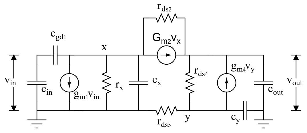
The simplified small-signal equivalent model of the core amplifier is shown in Figure 2, where, cin = cgs1, rx= r, cx= c, Gm2= g, cy= c, cout = c. Now ignoring the very high-frequency pole at node y, the above small-signal model can be approximated with a second-order system where the dominant pole is at the output high impedance node while the non-dominant pole is accompanied with the folded node (x).
Hence the following expressions can be derived. The open-loop dc gain,
| (3) |
The low frequency pole (p) at the output,
| (4) |
Where, rout =
The high frequency (p) second pole,
| (5) |
The resultant UGB (Unity Gain Bandwidth) of the core amplifier,
| (6) |
4 Design methodology
The low power budget of 2 mW, defined by the application, roughly sets the maximum bias current for the CSA to be 400 A. The authors have set I1 to be 50 A, and I2 to be 400 A and reasonable Vdsat for each transistor according to the bias current, voltage swing, and transistor specific operating region requirements. Since M3 carries the maximum current, it has been assigned a larger Vdsat of 500 mV, while the cascode transistor M2 has been provided with 200 mV of Vdsat. Vdsat of 300 mV has been set for M4 and M5 in the current mirror load due to the lower mobility of the PMOS transistors. Vb1 and Vb2 are biased at V and VDD - V respectively to ensure the output swing of the core amplifier is VDD - V. A very low Vdsat of 50 mV has been considered for the input transistor M1, to obtain a high gm value with a low bias current. Aspect ratios are calculated based on the equation shown in Table 1, which are later optimized to achieve the high dc loop gain (Av0>80 dB) for maximum charge transfer from the detector to the CSA, low input impedance (Zin), and subsequently low crosstalks among the adjacent channels [17]. Minimum allowed transistor length (Lmin) is used for the input transistor (M1) to ensure maximum g (”Figure of Merit”) [14, 18]. The cascode transistor (M2) is designed with a higher aspect ratio to place the non-dominant pole of the core amplifier away from the 3-dB frequency of the closed-loop system of CSA coupled with a detector, discussed in section 4.1 and A. M3 and M5 are designed with larger L and higher Vdsat to reduce their noise contribution. The calculated and the final aspect ratio of the transistors are given in Table 1. An aspect ratio of 0.5 is kept for the feedback transistors (M) to ensure they work in the linear region.
| Transistor | Id (A) | Keff= (A/V2) | Vdsat (V) | Calculated (W/L) =2Id/(KV) | Final (W/L) | Operating Region∗ |
| M1 | 350 | 30 | 50m | 10000 | 10000 | 3 |
| M2 | 50 | 100 | 200m | 25 | 100 | 2 |
| M3 | 400 | 100 | 500m | 32 | 50 | 2 |
| M4 | 50 | 30 | 300m | 40 | 50 | 2 |
| M5 | 50 | 30 | 300m | 40 | 50 | 2 |
3: Sub-threshold region (edge of weak/moderate inversion), 2: Saturation region.
Table 2 provides the dc bias voltages at different nodes in the circuit.
| Sr Number | Node | dc bias point (V) |
|---|---|---|
| 1. | Input | 3.985 |
| 2. | x | 0.42 |
| 3. | Out | 3.985 |
| 4. | y | 4.5 |
| 5. | V | 1.5, 3.2 |
4.1 Design calculation
In this design for the core amplifier, with the value of g 7 mS, c 4.5 pF, the value of f0 is 247 MHz. According to 4 and 5, the low-frequency pole (p) of the core amplifier is at 1.8 kHz, while the high-frequency pole (p) is at 50 MHz with r 20 MΩ, c 3.5 pF, and G 1.1 mS. The calculated open-loop dc gain is 103 dB. The second-order transfer function of the closed-loop system incorporating the CSA coupled with a silicon detector (as shown in A), involves two poles prfcf due to the feedback network (Rf and Cf) and pcfb due to the network involving Cf, Ct, the core amplifier. The location of these two poles can be calculated as (considering negligible load at the output),
| (7) |
| (8) |
Where, with detector capacitance of 40 pF, Ct 45 pF. The closed-loop bandwidth (-3dB frequency) is evaluated by Equation 8, which is also the unity gain frequency of the charge feedback loop. The dominant pole (Equation 7) is around 2.7 kHz, and the non-dominant pole (p) sits at a frequency around 50 MHz. The overall phase margin of the system is then given by (Equation 9).
| (9) |
5 Simulation results
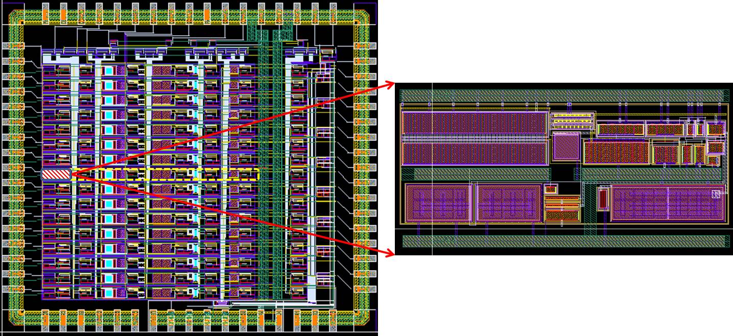
The physical design of the CSA has been carried out using an inter-digitized layout for the large input transistor [12], using multiple contacts, frequent substrate contact, and guard rings to minimize the parasitic noise due to the resistive poly gate and distributed substrate resistance. Figure 3 shows the layout view of the designed CSA (415 m x 200 m) as a part of the 16 channel pulse processing ASIC (5.6 mm x 5.2 mm) developed as FEE for Si-W calorimeter.
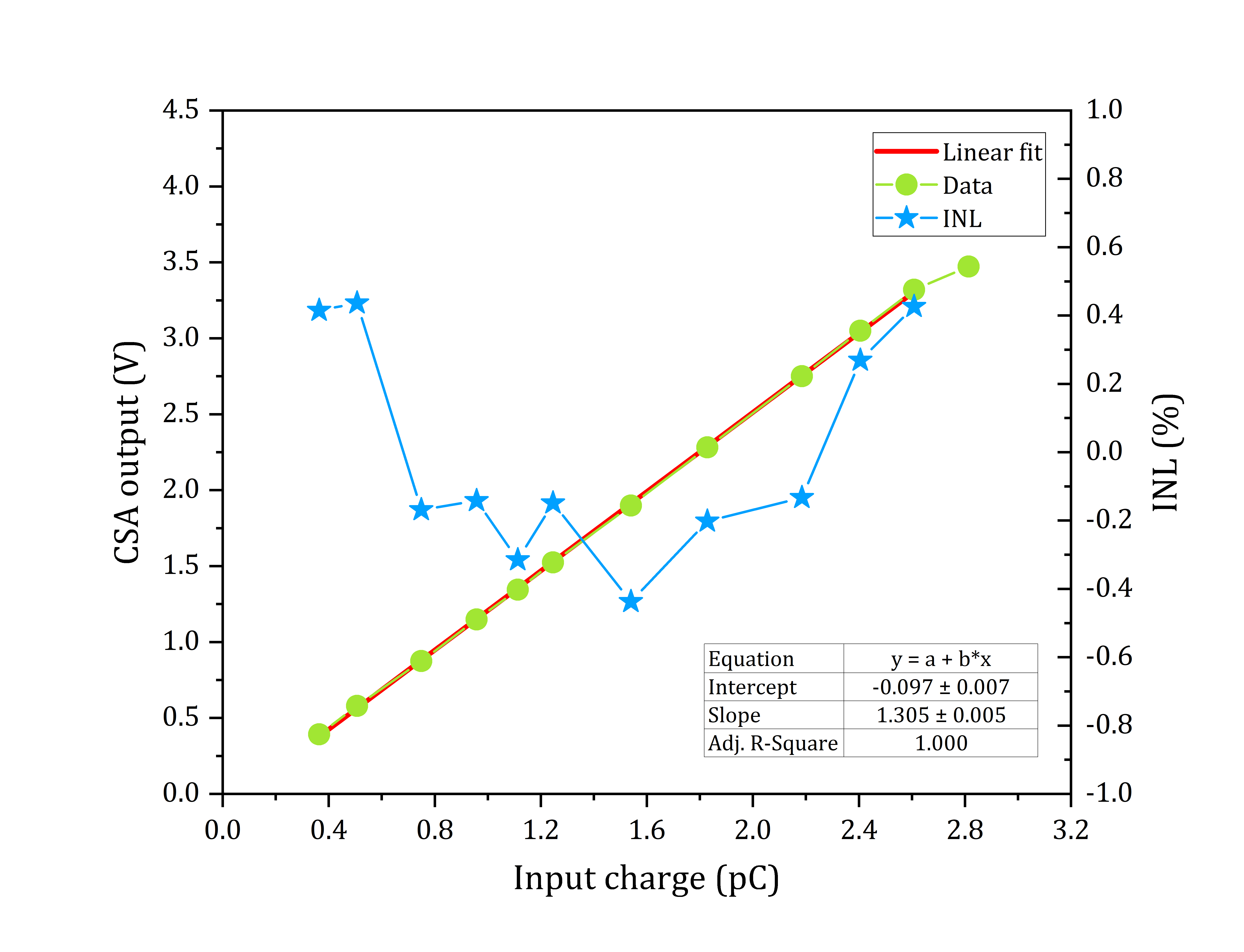
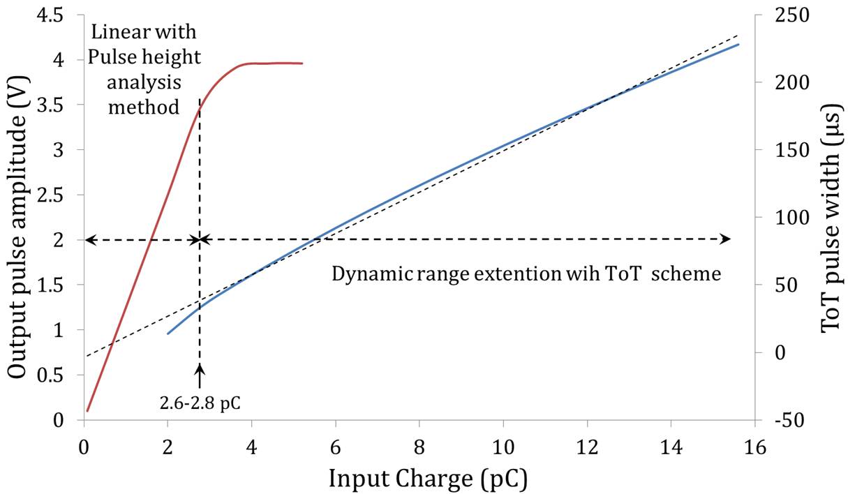
The simulations of the CSA were carried out with the silicon extracted view across all the design corners provided by the foundry. To inject a test charge in the simulation, a tail pulse (using an exponential voltage pulse) was used with a test (coupling) capacitor (0.8 pF to have the closed-loop voltage gain of 1) connected in series with the CSA input. The transient response at the CSA output is shown in Figure 4. The output dc point of the CSA is biased at 3.985 V and a linear behaviour of the CSA circuit can be seen up to a injected test charge of 2.8 pC (corresponds to input voltage of 3.5 V into a 0.8 pF coupling capacitor).
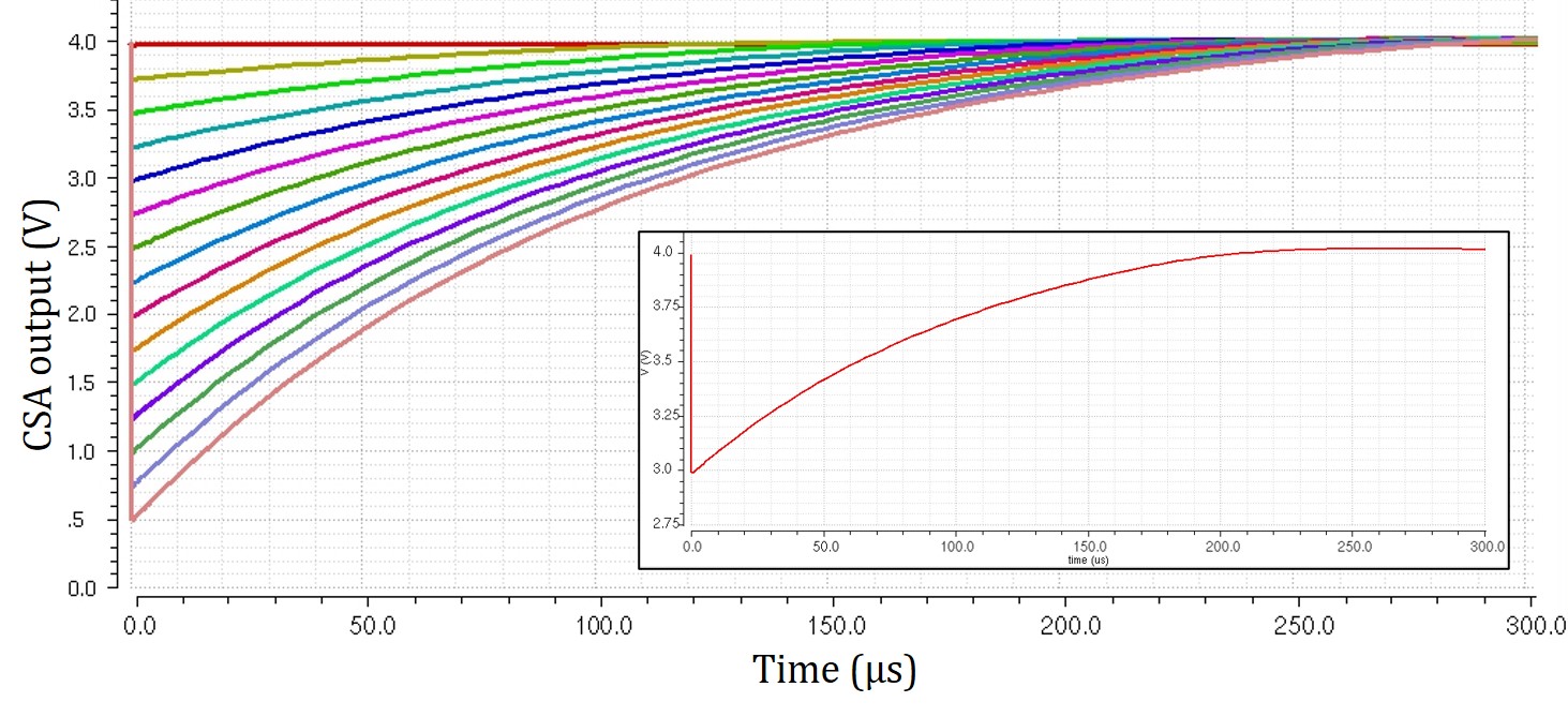
Table 3 summarizes the salient design features of the simulated CSA with a 40 pF detector capacitance (Cdet).
| Sr. No | Parameter | Value |
|---|---|---|
| 1. | dc Loop gain | 83.73 dB |
| 2. | Phase margin | 86 degree |
| 3. | Unity gain frequency | 3.33 MHz |
| 4. | Power consumption | 2.3 mW |
| 5. | ENC∗ (Cdet = 0 pF) | 500 e- |
| 6. | Noise slope∗ | 18 e-/pF |
| 7. | Conversion gain | 1.25 mV/fC |
| 8. | Area | 415 m x 200 m |
| 9. | Technology | 0.35 m CMOS |
| 10. | Supply | +5V, GND |
when followed by a CR-RC2 filter of 1.2 s peaking time
6 Test Results
As a part of a bigger FEE ASIC, the CSA was fabricated in a 0.35 m CMOS technology and packaged in CLCC 68. The FEE ASIC consists of 16 pulse processing channels, where each channel consists of CSA, semi-gaussian pulse shaper, track & hold and gain stage. For diagnostic and calibration purposes, all the individual stage output of a particular channel was taken out to the package pins. The fabricated CSA has been functionally tested utilizing the calibration channel in the packaged ASIC in the laboratory. The linearity of the wide swing CSA has been measured by observing the output response on the oscilloscope with increasing input voltage pulse in series with a coupling capacitor (to inject charge) and plotted in Figure 5. The linear response of the CSA is satisfactory with an Integral Non Linearity better (INL) than 0.4% up to 2.6 pC of input charge (corresponding to an output swing of 3.3 V). The measured conversion/charge gain is 1.3 mV/fC, while the ENC and noise slope shows a higher value of 820 e- and 25e-/pF respectively from that achieved in the simulation. This results in a dynamic range of 79 dB. The cross-talk measured at the final output of the FEE ASIC is 0.6%. Table 4 summarizes the test results of the CSA.
| Sr. No | Parameter | Value |
|---|---|---|
| 1. | ENC∗ (Cdet = 0 pF) | 820 e- |
| 2. | Noise slope∗ | 25 e-/pF |
| 3. | INL | better than 0.4% up to 2.6 pC |
| 4. | Dynamic range | 79 dB |
| 5. | Conversion gain | 1.3 mV/fC |
| 6. | Cross-talk∗∗ | 0.6% |
when followed by a CR-RC2 filter of 1.2 s peaking time
Measured at the final output of the FEE ASIC
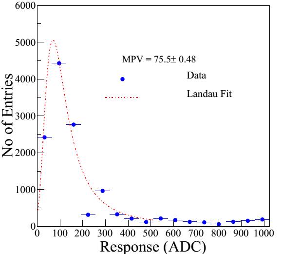
The ASIC has been validated at the SPS beamline, CERN as FEE readout for the prototype forward calorimeter (FOCAL) [19], a proposed electromagnetic calorimeter as part of the ALICE upgrade. The response of the prototype calorimeter was linear up to incident energy of 90 GeV for an electron beam validating the wide swing FEE. The MIP response, measured with a 120 GeV of pion beam, is shown in Figure 6, which signifies the low noise performance of the ASIC. These results, as depicted in Figure 5 and Figure 6, validate the wide dynamic range CSA, of this paper, as the first stage of the FEE ASIC.
7 Conclusion
A wide swing CSA has been designed in a 0.35 m CMOS technology, fabricated, and tested. The architecture of the CSA is based on a folded cascode amplifier as the input stage and wide swing current mirrors as the load. The CSA, designed with a reasonably low power budget of 2.3 mW, has shown a linear response up to 2.6 pC of input charge with a dynamic range of 79 dB. The design has been fabricated as a part of a 16 channel pulse processing FEE ASIC. The ASIC was successfully validated at the SPS beamline, CERN, as a FEE readout for the prototype FOCAL detector, using a 120 GeV pion beam and up to 90 GeV of an electron beam. For an anticipated input signal of positive polarity in the target application for a known detector biasing scheme, this design has achieved an enlarged negative output swing by biasing towards one supply rail and utilizing the voltage range towards the other supply rail. Similarly, for the opposite polarity (negative) of a large input signal, the same design architecture reported in this paper can be utilized using the complementary types of transistors (shown in B). Moreover, the combination of the wide swing CSA of this paper and the ADC+ToT [10] technique can result in FEE with an even higher dynamic range (shown in C).
8 Acknowledgements
The authors are thankful to Bhabha Atomic Research Centre, Mumbai – 400085, and Variable Energy Cyclotron Centre, Kolkata – 700097 India, for supporting the research work. The authors would also like to thank all the crew members of the SPS beamline for the excellent quality of beam for the detector test and ALICE-FOCAL collaboration for the support during the tests.
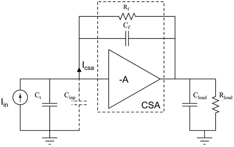
Appendix A The CSA and the silicon detector
The generalized circuit configuration of the CSA with silicon detector at the input and the output load is shown in Figure 7. The total signal charge Q generated inside the detector (due to signal current Iin(t)) will be distributed between the total input capacitance Ct (Cdet+Cf+Cgs1+Cgd1) [13] and the dynamic input impedance Cinp of the CSA. The dynamic input impedance of the CSA will be resistive and Cinp = 1/(Cf) [20], where =2f0 and f0 corresponds to the unity-gain bandwidth of the core amplifier with the output load. The expression for Icsa, the current getting integrated across the Cf can be written as,
| (10) |
Where, = Ct/( Cf). Now,
| (11) |
Where, = Rf Cf. Rearranging,
| (12) |
Equation 12 gives the transfer function of the closed-loop system involving the detector and the CSA. The transfer function involves two time constants ( and ), one due to the feedback network (Rf, Cf) and the other due to the network involving Cf, Ct, the core amplifier. Since the detector current can be approximated as a Dirac impulse with an integrated area of Q, the Laplace transform of Iin(t) is equal to Q. Hence, it can be written as,
| (13) |
Taking the inverse Laplace transform,
| (14) |
The expression of Equation 14 is the general form of the time-domain response of the CSA output, where AQ = 1/Cf is the charge gain of the CSA. and are the time constants associated with the two poles prfcf and pcfb. The value of the pole pcfb (= (Cf)/(2Ct)) happens to be equal to the unity gain frequency of the charge feedback loop. So, to ensure stability, the high-frequency poles of the core amplifier (p) need to be designed away from pcfb. Equation 14 shows the fall time is determined by the feedback resistor and capacitor (RfCf), while the rise time is inversely proportional to the product of f0 and Cf and directly proportional to Ct.
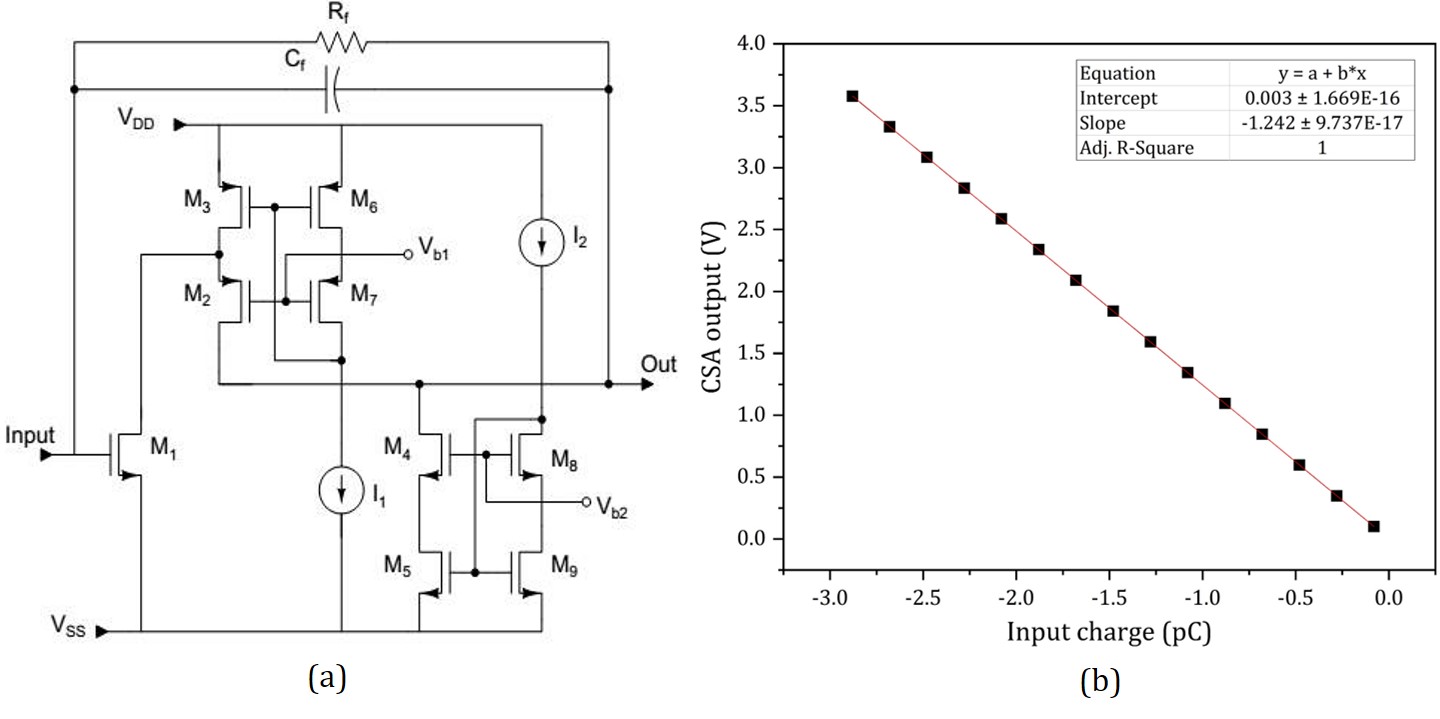
Appendix B Wide swing CSA for the opposite polarity of an input signal
Using the same architecture as shown in section 2, the design of CSA can be modified to accommodate a large negative swing of the input signal. All the transistors of Figure 1b need to be changed to their complementary type respectively. Figure 8a shows a simplified schematic of the same. The linear performance of the circuit has been plotted in Figure 8b.
Appendix C Wide swing CSA with ToT to further improve the dynamic range
As a proof-of-concept of the dynamic range enhancement technique with the combination of the ToT scheme and the conventional pulse amplitude analysis using ADC, the designed CSA of this paper has been simulated with a much larger amplitude of the input signal than the original linear range of 2.6 pC. Figure 9 shows the transient response of the CSA with a parametric sweep of the input signal from low to very high amplitude.
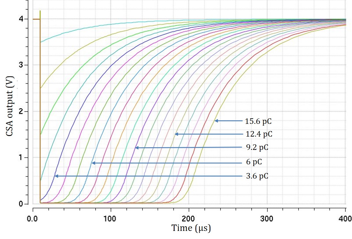
Time over threshold pulse width has been measured from Figure 9 by keeping a threshold voltage of 2V (where the CSA output gets saturated over 3.5V) and plotted in Figure 10. It can be interpreted that the linear operating range of the CSA is enhanced up to more than 15 pC with reasonable linearity.
References
- [1] L. Royer, S. Manen, P. Gay, Signal processing for high granularity calorimeter: Amplification, filtering, memorization and digitalization, Journal of Instrumentation 5 (12). doi:10.1088/1748-0221/5/12/C12014.
-
[2]
S. Muhuri, S. Mukhopadhyay, V. B. Chandratre, M. Sukhwani, S. Jena, S. A. Khan,
T. K. Nayak, J. Saini, R. N. Singaraju,
Test and
characterization of a prototype silicon-tungsten electromagnetic
calorimeter, Nuclear Instruments and Methods in Physics Research, Section
A: Accelerators, Spectrometers, Detectors and Associated Equipment 764 (2014)
24–29.
doi:10.1016/j.nima.2014.07.019.
URL http://dx.doi.org/10.1016/j.nima.2014.07.019 -
[3]
S. Muhuri, S. Mukhopadhyay, V. B. Chandratre, T. K. Nayak, S. K. Saha,
S. Thakur, R. N. Singaraju, J. Saini, A. van den Brink, T. Chujo, R. N.
Patra, M. van Leeuwen, S. A. Khan, M. Sukhwani, G.-J. Nooren, T. Peitzmann,
Fabrication and beam
test of a silicon-tungsten electromagnetic calorimeter, Journal of
Instrumentation 15 (03) (2020) P03015—-P03015.
doi:10.1088/1748-0221/15/03/p03015.
URL https://doi.org/10.1088/1748-0221/15/03/p03015 -
[4]
G. Mavromanolakis, CALICE
silicon-tungsten electromagnetic calorimeter, Pramana 69 (6) (2007)
1063–1067.
doi:10.1007/s12043-007-0228-9.
URL https://doi.org/10.1007/s12043-007-0228-9 - [5] J. Barkeloo, J. Brau, M. Breidenbach, R. Frey, D. Freytag, C. Gallagher, R. Herbst, M. Oriunno, B. Reese, A. Steinhebel, D. Strom, A silicon-tungsten electromagnetic calorimeter with integrated electronics for the International Linear Collider, Journal of Physics: Conference Series 1162 (1). doi:10.1088/1742-6596/1162/1/012016.
-
[6]
J. Borg, S. Callier, D. Coko, F. Dulucq, C. de La Taille, L. Raux, T. Sculac,
D. Thienpont,
SKIROC2_CMS an
ASIC for testing CMS HGCAL, Journal of Instrumentation 12 (02) (2017)
C02019—-C02019.
doi:10.1088/1748-0221/12/02/c02019.
URL https://doi.org/10.1088/1748-0221/12/02/c02019 - [7] S. Callier, F. Dulucq, C. De La Taille, G. Martin-Chassard, N. Seguin-Moreau, SKIROC2, front end chip designed to readout the Electromagnetic CALorimeter at the ILC, Journal of Instrumentation 6 (12). doi:10.1088/1748-0221/6/12/C12040.
- [8] V. Bonvicini, G. Orzan, G. Zampa, N. Zampa, CASIS1.1: A very high dynamic range frontEnd electronics with integrated cyclic ADC for calorimetry applications, IEEE Nuclear Science Symposium Conference Record 2 (2007) 1078–1081. doi:10.1109/NSSMIC.2007.4437196.
-
[9]
T. Gunji,
Current
status and future plans of ALICE FOCAL project.
URL http://www.cns.s.u-tokyo.ac.jp/$∼$gunji/tmp/focal/gunji$_$v0.pptx -
[10]
P. Rubinov,
High granularity
calorimeter(HGC) readout.
URL https://indico.cern.ch/event/681247/contributions/2929049/attachments/1639225/2616690/Rubinov$_$ACES$_$2018$_$short.pdf -
[11]
Damien Thienpont on behalf of the HGC collaboration,
CMS
HG-CAL FEE 2016 - krakow.
URL https://indico.cern.ch/event/522485/contributions/2145685/attachments/1284214/1909479/CMS$_$HGCAL$_$FEE16-Krakow.pdf - [12] B. Razavi, Design of Analog CMOS Integrated Circuits, IInd Edition, Mc Graw Hill Education, 2017.
- [13] W. Sansen, Z. Y. Chang, Limits of Low Noise Performance of Detector Readout Front Ends, IEEE Transactions on Circuits and Systems 37 (11) (1990) 1375–1382. doi:10.1109/31.62412.
- [14] P. O’Connor, G. De Geronimo, Prospects for charge sensitive amplifiers in scaled CMOS, Nuclear Instruments and Methods in Physics Research, Section A: Accelerators, Spectrometers, Detectors and Associated Equipment 480 (2-3) (2002) 713–725. doi:10.1016/S0168-9002(01)01212-8.
- [15] D. J. Comer, D. T. Comer, Using the Weak Inversion Region to Optimize Input Stage Design of CMOS Op Amps, IEEE Transactions on Circuits and Systems II: Express Briefs 51 (1) (2004) 8–14. doi:10.1109/TCSII.2003.821517.
- [16] D. J. Comer, D. T. Comer, Operation of analog MOS circuits in the weak or moderate inversion region, IEEE Transactions on Education 47 (4) (2004) 430–435. doi:10.1109/TE.2004.825537.
- [17] Hugo Daniel Hernandez Herrera, Noise and psrr improvement technique for tpc readout front-end in cmos technology, a phd thesis.
- [18] International Atomic Energy Agency, IAEA-TECDOC-363: Selected topics in nuclear electronics, Tech. rep., Vienna (1986).
- [19] ALICE Collaboration, Letter of intent: A forward calorimeter (focal) in the alice experiment, cern-lhcc-2020-009, lhcc-i-036, Tech. rep., CERN, Geneva (Jun 2020).
- [20] H. Spieler, Semiconductor Detector Systems, OXFORD UNIVERSITY PRESS.