Giant voltage amplification from incipient ferroelectric states
Ferroelectrics subject to suitable electric boundary conditions present a steady negative capacitance response. When the ferroelectric is in a heterostructure, this behavior yields a voltage amplification in the other elements, which experience a potential difference larger than the one applied, holding promise for low-power electronics. So far research has focused on verifying this effect and little is known about how to optimize it. Here we describe an electrostatic theory of ferroelectric/dielectric superlattices, convenient model systems, and show the relationship between the negative permittivity of the ferroelectric layers and the voltage amplification in the dielectric ones. Then, we run simulations of PbTiO3/SrTiO3 superlattices to reveal the factors most strongly affecting the amplification. In particular, we find that giant effects (up to 10-fold increases) can be obtained when PbTiO3 is brought close to the so-called “incipient ferroelectric” state.
Since its revival in 2008Salahuddin and Datta (2008), the negative capacitance (NC) response of ferroelectrics has been a focus of attention. In principle, all materials must present a positive global capacitance or dielectric constant, a necessary condition for thermodynamic stability. Nevertheless, local NC states can be obtained in a variety of waysÍñiguez et al. (2019). Most interestingly, by placing a ferroelectric in contact with a dielectric, we can prevent it from reaching its lowest-energy state (homogenous polarization), forcing it to display a different order of relatively high energy. Such a frustrated ferroelectric will typically display a steady NC response upon application of an electric fieldBratkovsky and Levanyuk (2001, 2006); Íñiguez et al. (2019). This has been shown in detail for ferroelectric/dielectric superlattices that have emerged as model systems in the fieldZubko et al. (2016); Yadav et al. (2019); Das et al. (2021); Pavlenko et al. (2022).

To understand steady-state NC, let us consider the superlattice in Fig. 1, where ferroelectric (f) and dielectric (d) layers repeat periodically along the stacking direction . In the absence of free carriers, the continuity of the component of the displacement vector implies , where is the superlattice displacement while and are the layer vectors (we omit the subscript for simplicity). Using the definitions in Fig. 1, this yields
| (1) |
where is vacuum permittivity, is the superlattice polarization, is the external electric field along , and the total field in layer ( f, d) is
| (2) |
Further, since we can write
| (3) |
which shows that induced fields appear when the local and global polarizations differ. For the f-layer we typically have , so that opposes ; this is the so-called “depolarizing field”.
Because of the superlattice periodicity, the total voltage associated to the induced fields must be null, which implies . This means that there is no net depolarizing field, being the only macroscopic field acting on the system.
To examine the response to a variation of the external field , it is useful to introduce a quantity we call the “screening factor”, defined for the f-layer as
| (4) |
Here we use the primed susceptibilities , which are all but guaranteed to be positive. (The change in polarization – local or global – will always follow the change in the external field. By contrast, the usual susceptibility of the f-layer involves the local field, and becomes negative in the NC regime.) The inverse permitivitty of the f-layer can then be written as
| (5) |
Further, as detailed in Supplementary Note 1, we can derive the voltage response of the dielectric layer as
| (6) |
Voltage amplification (VA) corresponds to . This key quantity is fully determined by trivial geometric elements and the screening factor of the f-layer.
We now use these equations to discuss the dielectric response of a superlattice. Typically the ferroelectric layers will be more responsive than the dielectric ones, so that . From Eq. (3) we get that the induced depolarizing field will oppose , and hence . One usually expects the induced field to be smaller in magnitude than the applied one, so that . It follows that and , a behavior we may call normal.
Imagine we make the ferroelectric more responsive, e.g., by varying its temperature to approach a Curie point. Then, we can eventually reach a situation where the induced compensates the applied (), and the voltage drops exclusively in the dielectric layers (). The ferroelectric effectively behaves as a metal, and we call this “perfect screening”.
If we keep softening the f-layer so that , we access a regime where the ferroelectric “over-screens”: its response is so strong that the induced depolarizing field exceeds the applied one (). This yields NC () and VA in the dielectric ().
The above formulas show that NC and VA can be obtained from the layer polarizations, easily accessible from atomistic simulations. The so-called “second-principles” methodsWojdeł et al. (2013); sca (see Methods) have been key to explain NC in PbTiO3/SrTiO3 (PTO/STO) superlattices. Here we use said methods to monitor the dependence of NC and VA on the design variables offered by these artificial materials (layer thickness, epitaxial strain), unveiling a distinct strategy to obtain giant effects.
We study PTO/STO superlattices where the PTO and STO layers have a thickness of and perovskite cells, respectively, denoted / in the following. We consider and from 3 to 9, and investigate the response to small external fields along . We also vary the epitaxial strain between % to %, choosing the STO substrate as the zero of strain.
For computational feasibility we restrict ourselves to low temperatures (formally, 0 K) and work with periodically-repeated supercells that are relatively small in plane ( perovskite units). As argued below, this suffices to draw conclusions on the behavior of real materials at ambient conditions.

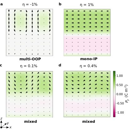
Let us first recall the main effect epitaxial strain has on PTO/STO superlattices, as obtained from our simulations. Figure 2a shows the ground state of the 6/6 system for %: it presents stripe domains in the PTO layer, with local polarizations along the out of plane (OOP) direction. This “multi-OOP” vortex-like state has been thoroughly studied in the literature Zubko et al. (2010); Aguado-Puente and Junquera (2012); Yadav et al. (2016); Zubko et al. (2016); Das et al. (2019); Baker and Bowler (2020).
For large enough tensile strains, we find the PTO layer displays a monodomain state with in-plane (IP) polarization (Fig. 2b). This simulated “mono-IP” configuration is characterized by . In realityDamodaran et al. (2017) one typically observes the so-called multidomain configuration, with local polarizations alternating between and . Our monodomain result is a consequence of the relatively small size of the simulation supercell.
Finally, Figs. 2c and 2d show states we find in some superlattices at intermediate values, where mono-IP and multi-OOP features “mix”, reminiscent of similar findings in the literatureDamodaran et al. (2017); Baker and Bowler (2020). In conclusion, apart from some non-essential size effects, our simulations capture the evolution of PTO/STO superlattices with epitaxial strain.

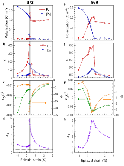
Figures 3a-d show detailed results for the 3/3 system. At compressive and slightly tensile strains, we get a multi-OOP solution similar to that of Fig. 2a, with and . As increases, we see an abrupt transition to the mono-IP phase with and . As typical of discontinuous transformations, the multi-OOP and mono-IP states are both stable for intermediate strains (gray area in the figure).
The global dielectric susceptibility is shown in Fig. 3b. As we increase in the multi-OOP state, we induce a maximum of , signaling the occurrence of an IP polar instability. In the case of the mono-IP state, it is that peaks as decreases, indicating a soft OOP polar mode. The mono-IP state also displays a peak in at %; this feature, associated to the STO layer and not essential here, is discussed in Supplementary Note 2 and Supplementary Figure 1.
Figure 3c shows the inverse permittivity (green) and screening factor (orange) of the f-layer. For all considered strains we get and the associated over-screening (). Further, Fig. 3d shows the corresponding VA in the d-layer, with reaching values as high as 12 when the mono-IP state approaches its stability limit. This giant amplification is related to the maximum in (panel b), in turn connected to the OOP polar instability of the PTO layer. In contrast, the destabilization of the multi-OOP state upon increasing – which involves a anomaly – does not result in any feature in or .
As shown in Figs. 3e-h, the 9/9 superlattice presents a similar behavior, the main difference being that we find no values where two states can exist. Instead, for between 0.0 % and 0.8 % we see a gradual transformation from multi-OOP to mono-IP, with the occurrence of the mixed state mentioned above (Figs. 2c and 2d). The small jump in around % is related to the occurrence of an IP polarization in the STO layer (not relevant here; see Supplementary Note 2 and Supplementary Figure 2).
The 9/9 superlattice displays its largest NC response in this intermediate region, reaching 5-fold amplifications at the transition point between the mono-IP and mixed states. The VA extends into the mono-IP region.
In contrast, the multi-OOP state of the 9/9 superlattices shows a different behavior: see e.g. at % in Fig. 3h. In this regime, the PTO layer is in a very stable (stiff) multidomain configuration, while the in-plane compression makes STO electrically soft along . Hence, the roles reverse and the STO layer displays NC. (See Supplementary Note 3 for more.) A similar behavior has been predicted in BaTiO3/SrTiO3 superlatticesWalter et al. (2020).

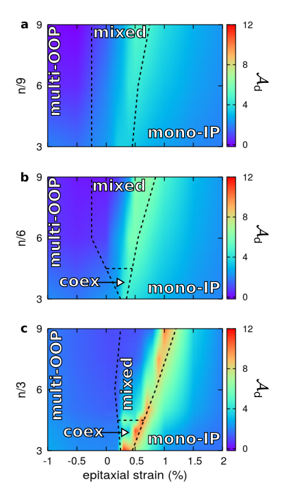
We run the same study for a large collection of superlattices; Figure 4 summarizes our results.
We find that the transition region between the multi-OOP and mono-IP states becomes wider for thicker PTO. This reflects the fact that broader PTO layers can accommodate more complex dipole orders, as the one occurring in the mixed state. (This is consistent with recent results in the literature, e.g. the occurrence of supercrystals in PbTiO3/SrRuO3 superlattices with PTO layers above 15 cellsHadjimichael et al. (2021).)
The mixed state is also favored by thicker STO layers. This effect is more subtle, and probably related to the fact that the stray fields are expelled from the STO layer as it thickens. This aspect is not essential here and we do not pursue it.
Most importantly, Fig. 4 confirms that the strongest amplifications occur at the stability limit of the mono-IP state. It also shows that the multi-OOP region is comparatively unresponsive. Let us now get insight into the physical underpinnings of these behaviors.
As captured by Eqs. 4 and 6, VA is essentially determined by the screening factor of the f-layer, which in turn depends on the difference in dielectric response between layers. For example, for the 3/3 superlattice at % we get , with and . This value may seem small; indeed, the ferroelectric is close to developing an OOP polar instability and, in such conditions, one expects susceptibilities Lines and Glass (1977); Graf and Íñiguez (2021). By contrast, the computed is surprisingly large, as our model for STO yields for the pure material. (Our simulated STO is relatively stiff as compared to experimentZubko et al. (2016); not essential here.)
The reason for these surprising susceptibilities can be traced back to the electrostatic requirement that . This leads all layers to respond similarly to an external field, to minimize the depolarizing fields. Thus, we expect . For example, for the 6/6 superlattice at %, which does not display VA, we obtain and (Supplementary Figure 3). Then, when we move to a region of the phase diagram where the f-layer presents an OOP instability, the energy gain associated to the development of overwhelms the cost of creating a depolarizing field. Hence, the difference between and grows a little, which suffices to yield large VA values.
The largest amplifications correspond to the region marking the limit of stability of the mono-IP state. We can say that, in this area, the f-layers are in an “incipient ferroelectric” stateÍñiguez et al. (2019); Walter et al. (2020): they are unstable against the development of an homogeneous OOP polarization whose occurrence is precluded by the presence of the d-layers. Eventually, as we move towards negative values, the multi-OOP polar instability freezes in, leading to either a pure multi-OOP state or a mixed state, and progressively hardening the -polarized ferroelectric soft mode. (This resembles the competition between antipolar and polar orders in antiferroelectricsKittel (1951); Lu et al. (2020).) This incipient ferroelectric state corresponds to the idealized picture of monodomain NCSalahuddin and Datta (2008); Íñiguez et al. (2019); our results predict a realization of this archetype.

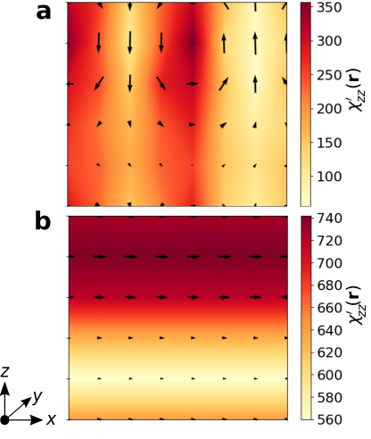
As shown in Fig. 5a and already reportedZubko et al. (2016); Yadav et al. (2019), the NC response of multi-OOP states mainly stems from the large dielectric response (large ) of the domain walls. By contrast, in the incipient ferroelectric state the NC response comes from the full volume of the f-layer (Fig. 5b). This partly explains the superior VA performance of the mono-IP state.
Our results suggest a strategy to obtain large VA: work with incipient ferroelectric states that will typically occur at the boundary between IP and OOP phases. Phase boundaries akin to the ones discussed here have been found experimentally in PTO/STO superlatticesDamodaran et al. (2017) and predicted in other ferroelectric/dielectric heterostructuresWalter et al. (2020); those are clear candidates to display giant VA effects. Note that, despite their limitations (low temperature, small supercells), our simulations capture the main physics of the IP-to-OOP transtion; thus, our conclusions can be expected to apply to experimentally relevant situations.
Additionally, our electrostatic formulas teach us that does not depend on the macroscopic permittivity (Eq. 6), while does (Eq. 5). As a consequence, one can have behaviors as that of the 3/3 system at % (Fig. 3): we get a very negative (panel c) not accompanied by a large (panel d). The reason is that this superlattice presents a small (panel b), which yields large and . By the same token, having a globally soft superlattice may result in a modest NC response of the f-layer, but this does not necessarily imply a small VA. Hence, there is no reason to disregard – for VA purposes – very responsive systems where small values of and have been measured or computedZubko et al. (2016); Yadav et al. (2019); Das et al. (2021). Rather, we must focus on the response difference between ferroelectric and dielectric layers, as captured by the screening factor .
Finally, let us stress that our conclusions for an idealized superlattice apply to other materials too. First, note that an infinite superlattice is equivalent to a ferroelectric/dielectric bilayer contacted with good electrodes, so there is no net depolarizing field. Second, NC is perfectly compatible with non-ideal electrodes and depolarizing fieldsBratkovsky and Levanyuk (2006); in fact, these fields reflect the electrostatic frustration at its origin. Hence, we expect our conclusions to apply to real systems where the development of an homogeneous polar state is precluded, including field-effect transistors featuring a ferroelectric/semiconductor bilayer.
We hope this work will bring an impetus to the study of negative capacitance, shifting the focus to the quantification and optimization of voltage amplification.
Methods
The second-principles simulations are performed using the SCALE-UP package Wojdeł et al. (2013); sca and the same approach as previous studies of PTO/STO superlatticesDas et al. (2019); Pereira Gonçalves et al. (2019); Zubko et al. (2016). The superlattice models are based on potentials for the pure bulk compounds – fitted to first-principles resultsWojdeł et al. (2013) – and adjusted for the superlattices as described in Ref. Zubko et al., 2016.
We study a collection of superlattices with layer thicknesses . Further, we consider an isotropic epitaxial strain between % and 3 %, where the STO square substrate (with lattice constant of 3.901 Å) is taken as the zero of strain.
We work with a simulation supercell that contains perovskite unit cells in the plane (perpendicular to the stacking direction). In the direction, only 1 superlattice period is considered. Periodic boundary conditions are assumed.
In order to find the lowest-energy state of an superlattice at a given and electric field value, we relax the atomic structure by performing Monte Carlo (MC) simulated annealings. During the annealings, all atomic positions and strains are allowed to vary, except for the in-plane strains imposed by the substrate. From the resulting atomic structures, we compute local electric dipoles within a linear approximation (i.e., we consider the atomic displacements with respect to the high-symmetry reference structure and multiply them by their corresponding Born charge tensors), as customarily done in second-principles studiesZubko et al. (2016); Pereira Gonçalves et al. (2019).
To compute responses, a small external field of 0.2 MV cm-1 is considered. We checked that this field is small enough to obtain susceptibilities and the other relevant quantities within a linear approximation.
References
- Salahuddin and Datta (2008) S. Salahuddin and S. Datta, Nano Letters 8, 405 (2008).
- Íñiguez et al. (2019) J. Íñiguez, P. Zubko, I. Luk’yanchuk, and A. Cano, Nature Reviews Materials 4, 243 (2019).
- Bratkovsky and Levanyuk (2001) A. M. Bratkovsky and A. P. Levanyuk, Phys. Rev. B 63, 132103 (2001).
- Bratkovsky and Levanyuk (2006) A. M. Bratkovsky and A. P. Levanyuk, Appl. Phys. Lett. 89, 253108 (2006).
- Zubko et al. (2016) P. Zubko, J. C. Wojdeł, M. Hadjimichael, S. Fernandez-Pena, A. Sené, I. Luk’yanchuk, J. Triscone, and J. Íñiguez, Nature 534, 524 (2016).
- Yadav et al. (2019) A. K. Yadav, K. X. Nguyen, Z. Hong, P. García-Fernández, P. Aguado-Puente, C. T. Nelson, S. Das, B. Prasad, D. Kwon, S. Cheema, et al., Nature 565, 468 (2019).
- Das et al. (2021) S. Das, Z. Hong, V. A. Stoica, M. A. P. Gonçalves, Y. T. Shao, E. Parsonnet, E. J. Marksz, S. Saremi, M. R. McCarter, A. Reynoso, et al., Nature Materials 20, 194 (2021), ISSN 1476-4660.
- Pavlenko et al. (2022) M. A. Pavlenko, Y. A. Tikhonov, A. G. Razumnaya, V. M. Vinokur, and I. A. Lukyanchuk, Nanomaterials 12 (2022).
- Wojdeł et al. (2013) J. C. Wojdeł, P. Hermet, M. P. Ljungberg, P. Ghosez, and J. Íñiguez, Journal of Physics: Condensed Matter 25, 305401 (2013).
- (10) SCALE-UP, an implementation of second-principles density functional theory, https://www.secondprinciples.unican.es/.
- Zubko et al. (2010) P. Zubko, N. Stucki, C. Lichtensteiger, and J. M. Triscone, Physical Review Letters 104, 187601 (2010).
- Aguado-Puente and Junquera (2012) P. Aguado-Puente and J. Junquera, Phys. Rev. B 85, 184105 (2012).
- Yadav et al. (2016) A. K. Yadav, C. T. Nelson, S. L. Hsu, Z. Hong, J. D. Clarkson, C. M. Schlepuëtz, A. R. Damodaran, P. Shafer, E. Arenholz, L. R. Dedon, et al., Nature 530, 198 (2016).
- Das et al. (2019) S. Das, Y. L. Tang, Z. Hong, M. Gonçalves, M. McCarter, C. Klewe, F. Nguyen, K.X. Gómez-Ortiz, P. Shafer, E. Arenholz, V. Stoica, et al., Nature 568, 368 (2019).
- Baker and Bowler (2020) J. S. Baker and D. R. Bowler, Advanced Theory and Simulations 3, 2000154 (2020).
- Damodaran et al. (2017) A. R. Damodaran, J. D. Clarkson, Z. Hong, H. Liu, A. K. Yadav, C. T. Nelson, S. L. Hsu, M. R. McCarter, K. D. Park, V. Kravtsov, et al., Nature Materials 16, 1003 (2017).
- Walter et al. (2020) R. Walter, S. Prosandeev, C. Paillard, and L. Bellaiche, npj Computational Materials 6, 186 (2020).
- Hadjimichael et al. (2021) M. Hadjimichael, Y. Li, E. Zatterin, G. A. Chahine, M. Conroy, K. Moore, E. N. O. Connell, P. Ondrejkovic, P. Marton, J. Hlinka, et al., Nature Materials 20, 495 (2021).
- Lines and Glass (1977) M. E. Lines and A. M. Glass, Principles and Applications of Ferroelectrics and Related Materials, Oxford Classic Texts in the Physical Sciences (Clarendon Press, Oxford, 1977), ISBN 9780198507789.
- Graf and Íñiguez (2021) M. Graf and J. Íñiguez, Communications Materials 2, 60 (2021).
- Kittel (1951) C. Kittel, Phys. Rev. 82, 729 (1951).
- Lu et al. (2020) H. Lu, S. Glinsek, P. Buragohain, E. Defay, J. Íñiguez, and A. Gruverman, Advanced Functional Materials 30, 2003622 (2020).
- Pereira Gonçalves et al. (2019) M. A. Pereira Gonçalves, C. Escorihuela-Sayalero, P. García-Fernández, J. Junquera, and J. Íñiguez, Science Advances 5, eaau7023 (2019).
Acknowledgements
Work funded by the Luxembourg National Research Fund (FNR) through grants INTER/RCUK/18/12601980 (M.G, J.Í.) and FNR/C18/MS/12705883/REFOX/Gonzalez (H.A.), and by the United Kingdom’s EPSRC through grant EP/S010769/1 (P.Z.).