Design Space Exploration of Dense and Sparse Mapping Schemes for RRAM Architectures
Abstract
The impact of device and circuit-level effects in mixed-signal Resistive Random Access Memory (RRAM) accelerators typically manifest as performance degradation of Deep Learning (DL) algorithms, but the degree of impact varies based on algorithmic features. These include network architecture, capacity, weight distribution, and the type of inter-layer connections. Techniques are continuously emerging to efficiently train sparse neural networks, which may have activation sparsity, quantization, and memristive noise. In this paper, we present an extended Design Space Exploration (DSE) methodology to quantify the benefits and limitations of dense and sparse mapping schemes for a variety of network architectures. While sparsity of connectivity promotes less power consumption and is often optimized for extracting localized features, its performance on tiled RRAM arrays may be more susceptible to noise due to under-parameterization, when compared to dense mapping schemes. Moreover, we present a case study quantifying and formalizing the trade-offs of typical non-idealities introduced into 1-Transistor-1-Resistor (1T1R) tiled memristive architectures and the size of modular crossbar tiles using the CIFAR-10 dataset.
Index Terms:
Memristor, RRAM, In-Memory Computing (IMC), Deep Learning, Design Space ExplorationI Introduction
Hybrid mixed-signal RRAM IMC systems are being used to efficiently perform inference of linear and unrolled convolutional layers in DL systems [1, 2, 3, 4, 5]. In recent years, a number of different dense and sparse mapping schemes have been proposed to reduce the required number of devices to perform inference of pre-trained Artificial Neural Networks [6]. However, the efficacy of different dense and sparse mapping schemes is not well understood with respect to different circuit and device parameters, typical non-idealities, and network architectures.
While various hardware-aware training routines [8, 9, 10, 11] and generic search methodologies [12, 13] can be used to mitigate performance degradation when mapping pre-trained ANN architectures onto RRAM architectures, they are cumbersome, dependent on a pre-determined set of circuit and device parameters, and are not interpretable. Recently, Quantization-Aware Training (QAT) has demonstrated the ability to improve the performance of, and to robustly reduce the error of IMC implementations of pre-trained ANNs using RRAM devices with discrete conductance states [14, 15, 16]. However, it remains difficult to quantify performance trade-offs and limitations of dense and sparse mapping schemes without simulating them. In this paper, we present an extended DSE methodology to explore the efficacy of dense and sparse mapping schemes for RRAM architectures. Our methodology is able to explore the efficacy of dense and sparse mapping schemes for RRAM architectures without the requirement to simulate multiple dense and sparse schemes. Using our methodology, we quantify the benefits and limitations of dense and sparse mapping schemes for four popular Convolutional Neural Network (CNN) architectures.
II Related Work
Related work in literature has attempted to quantify the various performance trade-offs in designing and implementing RRAM architectures with respect to many different device and circuit parameters. Xu et al. [17] studied RRAM architecture design, and primarily focused on the choices of different peripherals to achieve the best trade-off among performance, energy, and area. Niu et al. [18] performed a comprehensive analysis of issues related to reliability, energy consumption, area overhead, and performance. Xu et al. [19] investigated and discussed trade-offs involving voltage drop, write latency, and data patterns. Matthew et al. [20] presented a DSE framework to quantify trade-offs with respect to array sizes, write time and write energy. Recently, customizable simulation frameworks have been developed and used to simulate inference and/or training routines of RRAM architectures [21, 22, 23, 24].
III Preliminaries
III-A RRAM Crossbars
Modular crossbar tiles, comprised of smaller sized crossbar architectures with RRAM devices arranged in dual-column or dual-tile configurations, can be used to encode quantized analog weight-representations. By encoding Word Line (WL) inputs as voltages, Vector-Matrix Multiplications can be performed in [3], where analog dot products are realized along each of Bit Lines, by exploiting Ohm’s law, i.e, .
III-B Conventional and Sparse Mapping Schemes
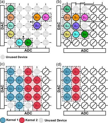
In Fig. 1, four popular conventional sparse (a,c) and dense (b,d) weight mapping schemes are depicted. For arbitrary crossbars adopting a differential weight mapping scheme, as depicted in Fig. 1 (b), interconnects can be rerouted at the cost of increased time complexity to reduce the required number of devices [7]. Specifically when mapping convolutional layers, as depicted in Fig. 1 (d), kernels can be mapped in a dense arrangement, at the cost of increased read/write operations.
III-C Sparsity of Traditional ANNs
It has been shown empirically that ANNs can tolerate high levels of sparsity, and this property has been leveraged to enable the deployment of state-of-the-art models in severely resource constrained environments, with no significant performance degradation [25, 26]. Sparsity is most commonly introduced using L1-regularization and Dropout layers. By increasing network sparsity, an appropriately optimized array can reduce the required number of RRAM devices, as well as the overhead of Digital-to-Analog Converters, Analog-to-Digital Converters, and peripheral circuitry.
IV Proposed DSE Methodology
We confine our proposed DSE search space to the following dimensions: the weight mapping scheme, I/O bit-width, tile size, maximum input encoding voltage, device/circuit non-idealities (see Section IV.B for further detail), mini-batch size, and regularization method(s). These can be categorized as network, mapping, or device/circuit related. Our proposed DSE methodology criteria consists of the following steps:
For each bit-width and network architecture to investigate, QAT is performed using a pre-determined dataset. Ranges of each dimension (for dimensions which are not fixed to a singular value) are determined. Using Simulation Program with Integrated Circuit Emphasis (SPICE)-based circuit simulation tools, or RRAM-based DL simulation frameworks, the test or validation set accuracy for the pre-determined dataset is determined using either (a) Bayesian Optimization, or (b) a grid-search, exploring the search space. Eqs. (1) – (3) are used to determine the number of required devices, tiles, and computational steps, for each configuration, after simulating one mapping scheme. Contour plots are generated to explore the efficacy of different network parameters, and device/circuit parameters, using the test or validation set accuracy as the objective function. A score is determined for each configuration, weighting the number of required devices, tiles, and the test and/or validation set accuracy. Scores are manually compared.
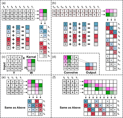
When the scheme depicted in Fig 1(b) was used, we assumed that convolutional kernels were mapped densely. Space requirements for convolutional and linear layers of the dense mapping schemes depicted in Fig 1(b) can be determined using routing algorithms, where the size of modular crossbar tiles and location of zero weights are known [7]. Space requirements for convolutional layers of sparse and dense mapping schemes depicted in Fig 1(c) and Fig 1(d) can be determined without being physically laid out and simulated using (1) and (2), respectively, where , , , and are defined in Fig 2. denotes dilation, denotes the number of kernels, and denotes the stride. For 1d-convolutional layers, .
| (1) | ||||
| (2) |
The required number of computational steps in Fig 1(d) can be determined using (3)
| (3) |
V A Case Study
In this Section, we present a case study investigating the performance of different 1T1R RRAM architectures used to perform inference of linear and unrolled convolutional layers within popular CNN architectures using the CIFAR-10 dataset. For all implementations, a dual-column differential weight representation scheme was adopted.
V-A Network Architectures and QAT
To ensure a sufficiently large design space was explored, we investigated the performance of four popular network architectures. A batch size of 256 and 257 training epochs were used for all implementations, with the RMSProp optimizer and a learning rate of 0.001512, which demonstrated significant performance empirically. To investigate the effect of network sparsity, for all implementations, the L1 weight-decay was set to 5e-4. The Xilinx Brevitas [27] library was used in conjunction with the PyTorch [28] Machine Learning (ML) library to train all baseline network architectures. The weight sparsity and test set accuracy of each baseline implementation is presented in Table I.
V-B Device Non-Idealities
In all simulations, the following device non-idealities were accounted for: device-to-device variability, a finite number of conductance states, and stuck and devices (including those that have failed to electroform). We note that, while only three non-ideal device characteristics were investigated, more could easily be added, such as conductance drift and endurance and retention characteristics [29].
| Architecture | Bit-Width | Zero Weight Values | Test Accuracy (%) |
|---|---|---|---|
| VGG-16 [30] | 4 | 189,020/15,239,872 (1.24%) | 86.24 |
| 6 | 237,869/15,239,872 (1.56%) | 87.96 | |
| 8 | 240,454/15,239,872 (1.58%) | 87.88 | |
| ResNeXt29 2x64d[31] | 4 | 109,100/9,103,552 (1.20%) | 85.70 |
| 6 | 341,462/9,103,552 (3.75%) | 85.89 | |
| 8 | 190,482/9,103,552 (2.09%) | 84.21 | |
| MobileNetV2 [32] | 4 | 74,318/2,261,824 (3.29%) | 87.57 |
| 6 | 95,521/2,261,824 (4.22%) | 88.48 | |
| 8 | 123,501/2,261,824 (5.46%) | 88.48 | |
| GoogLeNet [33] | 4 | 570,755/6,142,528 (9.29%) | 55.19 |
| 6 | 102,490/6,142,528 (1.67%) | 86.17 | |
| 8 | 266,513/6,142,528 (4.32%) | 86.72 |
V-C Modular Crossbar Tile Size
For all implementations, modular symmetric crossbar tiles were used to mitigate the effects of non-ideal device and circuit characteristics. We investigated the following modular crossbar tile sizes: (32 32), (64 64), (128 128), and (256 256).
| Configuration | Required Devices (RD) | Read/Write Operations (RWO) | Test Set Accuracy (TSA) (%) | Normalized Weighted Score | |||||||||||||||||||||||||||
|---|---|---|---|---|---|---|---|---|---|---|---|---|---|---|---|---|---|---|---|---|---|---|---|---|---|---|---|---|---|---|---|
| = [TSA / (RD RWO)]’ | |||||||||||||||||||||||||||||||
| Architecture |
|
Bit-Width |
|
|
|
|
|
|
|
|
|
||||||||||||||||||||
| 256/64 | 4 | 15,016x64x64 | 3,531x64x64 | 3,705x64x64 | 143x64 | 2,135x64 | 2,591x64 | 86.10 | 0.4947 | 0.1403 | 0.1098 | ||||||||||||||||||||
| VGG-16 | 256/32 | 6 | 60,063x32x32 | 14,077x32x32 | 14,818x32x32 | 566x32 | 8,048x32 | 10,340x32 | 87.86 | 0.2546 | 0.0758 | 0.0557 | |||||||||||||||||||
| 256/32 | 8 | 60,063x32x32 | 14,072x32x32 | 14,818x32x32 | 566x32 | 8,121x32 | 10,340x32 | 87.74 | 0.2543 | 0.0748 | 0.0557 | ||||||||||||||||||||
| 256/64 | 4 | 243,653x64x64 | 2,184x64x64 | 2,213x64x64 | 657x64 | 24,266x64 | 24,712x64 | 83.87 | 0.0055 | 0.0186 | 0.0180 | ||||||||||||||||||||
| ResNeXt29 | 64/64 | 6 | 243,653x64x64 | 2,070x64x64 | 2,213x64x64 | 657x64 | 22,681x64 | 24,712x64 | 86.08 | 0.0057 | 0.0217 | 0.0185 | |||||||||||||||||||
| 256/64 | 8 | 243,653x64x64 | 2,165x64x64 | 2,213x64x64 | 657x64 | 24,712x64 | 24,712x64 | 82.28 | 0.0054 | 0.0180 | 0.0176 | ||||||||||||||||||||
| 256/64 | 4 | 48,590x64x64 | 528x64x64 | 548x64x64 | 220x64 | 2,181x64 | 2,406x64 | 76.85 | 0.0878 | 0.8251 | 0.7182 | ||||||||||||||||||||
| MobileNetV2 | 256/32 | 6 | 194,257x32x32 | 2,092x32x32 | 2,191x32x32 | 875x32 | 8,525x32 | 9,524x32 | 88.71 | 0.0505 | 0.4914 | 0.4201 | |||||||||||||||||||
| 256/64 | 8 | 48,590x64x64 | 516x64x64 | 548x64x64 | 220x64 | 2,119x64 | 2,406x64 | 88.52 | 0.1014 | 1.0000 | 0.8283 | ||||||||||||||||||||
| 16/64 | 4 | 561,915x64x64 | 1,345x64x64 | 1,481x64x64 | 1,246x64 | 15,142x64 | 17,552x64 | 55.54 | 0.0000 | 0.0327 | 0.0254 | ||||||||||||||||||||
| GoogLeNet | 16/256 | 6 | 35,120x256x256 | 91x256x256 | 92x256x256 | 79x256 | 1,068x256 | 1,127x256 | 85.58 | 0.0050 | 0.1691 | 0.1584 | |||||||||||||||||||
| 16/128 | 8 | 140,479x128x128 | 354x128x128 | 371x128x218 | 312x128 | 4,207x128 | 4,417x128 | 86.58 | 0.0021 | 0.0888 | 0.0470 | ||||||||||||||||||||
V-D Results
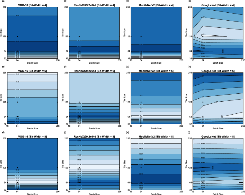
To apply our DSE methodology, we determined the optimal batch size and tile shape (of symmetric tiles) for inference, as depicted in Fig. 3. In addition, we reported the best of a normalized device-read/write-accuracy weighted score, alongside: the required number of devices, required number of read/write operations, and the test set accuracy. For each architecture and bit-width, the optimal batch and tile sizes were determined with respect to the test set accuracy. The performance of these configurations are presented in Table II. To simulate RRAM architectures, the MemTorch [21] simulation framework was used. The following fixed parameters were used to reduce the dimensionality of the explored design space: was sampled from a normal distribution with a mean of 100k and a standard deviation of 10,000. was sampled from a normal distribution with a mean of 10k and a standard deviation of 1,000. A maximum encoding input voltage of 0.3V was used [34], with a failure rate of stuck devices to of 0.5%, and a failure rate of stuck devices to of 0.5%. The range of terms used to compute the weighted score can be standardized to reduce biases, and depending on specific user requirements, different weightings can be applied.
VI Discussion and Conclusions
In Table II, it can be observed that MobileNetV2 with a batch size of 256 and a tile size of 64 achieved the best normalized weighted score. As can be seen in Fig. 3, for all network architectures other than GoogLeNet, the batch size used during inference had a negligible influence on the test set accuracy. Our empirical results indicate that for the investigated networks, symmetrical tiles with a size of where deemed optimal. For all network architectures, the optimal tile shape was found to be dependent on both the network architecture used and the bit-width. This suggests that the optimal tile size for pre-trained CNNs cannot easily be determined without performing an exploratory analysis. Despite being limited in scope, we believe that the case study in Section V demonstrates the effectiveness of our presented DSE methodology to investigate and determine dependencies between different search space dimensions.
References
- [1] M. Rahimi Azghadi, Y.-C. Chen, J. K. Eshraghian, J. Chen, C.-Y. Lin, A. Amirsoleimani, A. Mehonic, A. J. Kenyon, B. Fowler, J. C. Lee, and Y.-F. Chang, “Complementary Metal-Oxide Semiconductor and Memristive Hardware for Neuromorphic Computing,” Advanced Intelligent Systems, vol. 2, no. 5, p. 1900189, 2020.
- [2] M. R. Azghadi, C. Lammie, J. K. Eshraghian, M. Payvand, E. Donati, B. Linares-Barranco, and G. Indiveri, “Hardware Implementation of Deep Network Accelerators Towards Healthcare and Biomedical Applications,” IEEE Transactions on Biomedical Circuits and Systems, vol. 14, no. 6, pp. 1138–1159, 2020.
- [3] A. Amirsoleimani, F. Alibart, V. Yon, J. Xu, M. R. Pazhouhandeh, S. Ecoffey, Y. Beilliard, R. Genov, and D. Drouin, “In-Memory Vector-Matrix Multiplication in Monolithic Complementary Metal–Oxide–Semiconductor-Memristor Integrated Circuits: Design Choices, Challenges, and Perspectives,” Advanced Intelligent Systems, vol. 2, no. 11, p. 2000115, 2020.
- [4] X. Wang, M. A. Zidan, and W. D. Lu, “A Crossbar-Based In-Memory Computing Architecture,” IEEE Transactions on Circuits and Systems I: Regular Papers, vol. 67, no. 12, pp. 4224–4232, 2020.
- [5] P. Yao, H. Wu, B. Gao, J. Tang, Q. Zhang, W. Zhang, J. J. Yang, and H. Qian, “Fully Hardware-Implemented Memristor Convolutional Neural Network,” Nature, vol. 577, no. 7792, pp. 641–646, Jan. 2020.
- [6] Y. Zhou, B. Gao, C. Dou, M.-F. Chang, and H. Wu, “Chapter 14 - RRAM-Based Coprocessors for Deep Learning,” in Memristive Devices for Brain-Inspired Computing, ser. Woodhead Publishing Series in Electronic and Optical Materials, S. Spiga, A. Sebastian, D. Querlioz, and B. Rajendran, Eds. Woodhead Publishing, 2020, pp. 363–395.
- [7] F. Liu, W. Zhao, Y. Zhao, Z. Wang, T. Yang, Z. He, N. Jing, X. Liang, and L. Jiang, “SME: ReRAM-based Sparse-Multiplication-Engine to Squeeze-Out Bit Sparsity of Neural Network,” CoRR, vol. abs/2103.01705, 2021. [Online]. Available: https://arxiv.org/abs/2103.01705
- [8] L. Chen, J. Li, Y. Chen, Q. Deng, J. Shen, X. Liang, and L. Jiang, “Accelerator-Friendly Neural-Network Training: Learning Variations and Defects in RRAM Crossbar,” in Proceedings of the Design, Automation Test in Europe Conference Exhibition (DATE), 2017, pp. 19–24.
- [9] C. Lammie, O. Krestinskaya, A. James, and M. R. Azghadi, “Variation-aware Binarized Memristive Networks,” in Proceedings of the IEEE International Conference on Electronics, Circuits and Systems (ICECS), 2019, pp. 490–493.
- [10] M. E. Fouda, S. Lee, J. Lee, G. H. Kim, F. Kurdahi, and A. M. Eltawi, “IR-QNN Framework: An IR Drop-Aware Offline Training of Quantized Crossbar Arrays,” IEEE Access, vol. 8, pp. 228 392–228 408, 2020.
- [11] B. Zhang, L.-Y. Chen, and N. Verma, “Neural Network Training With Stochastic Hardware Models and Software Abstractions,” IEEE Transactions on Circuits and Systems I: Regular Papers, vol. 68, no. 4, pp. 1532–1542, 2021.
- [12] B. Li, L. Xia, P. Gu, Y. Wang, and H. Yang, “Merging the Interface: Power, Area and Accuracy Co-Optimization for RRAM Crossbar-Based Mixed-Signal Computing System,” in Proceedings of the Design, Automation Test in Europe Conference Exhibition (DATE), ser. DAC ’15. New York, NY, USA: Association for Computing Machinery, 2015.
- [13] O. Krestinskaya, K. N. Salama, and A. P. James, “Automating Analogue AI Chip Design with Genetic Search,” Advanced Intelligent Systems, vol. 2, no. 8, p. 2000075, 2020.
- [14] C. Song, B. Liu, W. Wen, H. Li, and Y. Chen, “A Quantization-Aware Regularized Learning Method in Multilevel Memristor-Based Neuromorphic Computing System,” in Proceedings of the IEEE Non-Volatile Memory Systems and Applications Symposium (NVMSA), 2017.
- [15] Y. Cai, T. Tang, L. Xia, M. Cheng, Z. Zhu, Y. Wang, and H. Yang, “Training Low Bitwidth Convolutional Neural Network on RRAM,” in Proceedings of the Asia and South Pacific Design Automation Conference (ASP-DAC), 2018, pp. 117–122.
- [16] T. Van Nguyen, J. An, and K.-S. Min, “Comparative Study on Quantization-Aware Training of Memristor Crossbars for Reducing Inference Power of Neural Networks at The Edge,” in Proceedings of the International Joint Conference on Neural Networks (IJCNN), 2021.
- [17] C. Xu, X. Dong, N. P. Jouppi, and Y. Xie, “Design Implications of Memristor-Based RRAM Cross-Point Structures,” in Proceedings of the Design, Automation Test in Europe Conference Exhibition (DATE), 2011.
- [18] D. Niu, C. Xu, N. Muralimanohar, N. P. Jouppi, and Y. Xie, “Design Trade-Offs for High Density Cross-Point Resistive Memory,” in Proceedings of the ACM/IEEE International Symposium on Low Power Electronics and Design, New York, NY, USA, 2012, p. 209–214.
- [19] C. Xu, D. Niu, N. Muralimanohar, R. Balasubramonian, T. Zhang, S. Yu, and Y. Xie, “Overcoming the Challenges of Crossbar Resistive Memory Architectures,” in Proceedings of the IEEE International Symposium on High Performance Computer Architecture (HPCA), 2015, pp. 476–488.
- [20] D. M. Mathew, A. L. Chinazzo, C. Weis, M. Jung, B. Giraud, P. Vivet, A. Levisse, and N. Wehn, “RRAMSpec: A Design Space Exploration Framework for High Density Resistive RAM,” in Embedded Computer Systems: Architectures, Modeling, and Simulation, D. N. Pnevmatikatos, M. Pelcat, and M. Jung, Eds. Cham: Springer International Publishing, 2019, pp. 34–47.
- [21] C. Lammie, W. Xiang, B. Linares-Barranco, and M. R. Azghadi, “MemTorch: An Open-source Simulation Framework for Memristive Deep Learning Systems,” CoRR, vol. abs/2004.10971, 2020. [Online]. Available: https://arxiv.org/abs/2004.10971
- [22] M. J. Rasch, D. Moreda, T. Gokmen, M. Le Gallo, F. Carta, C. Goldberg, K. El Maghraoui, A. Sebastian, and V. Narayanan, “A Flexible and Fast PyTorch Toolkit for Simulating Training and Inference on Analog Crossbar Arrays,” in Proceedings of the IEEE International Conference on Artificial Intelligence Circuits and Systems (AICAS), 2021.
- [23] X. Peng, S. Huang, H. Jiang, A. Lu, and S. Yu, “DNN+NeuroSim V2.0: An End-to-End Benchmarking Framework for Compute-in-Memory Accelerators for On-Chip Training,” IEEE Transactions on Computer-Aided Design of Integrated Circuits and Systems, vol. 40, no. 11, pp. 2306–2319, 2021.
- [24] C. Lammie, W. Xiang, and M. Rahimi Azghadi, “Modeling and simulating in-memory memristive deep learning systems: An overview of current efforts,” Array, vol. 13, p. 100116, 2022.
- [25] T. Gale, E. Elsen, and S. Hooker, “The State of Sparsity in Deep Neural Networks,” CoRR, vol. abs/1902.09574, 2019. [Online]. Available: http://arxiv.org/abs/1902.09574
- [26] J. K. Eshraghian, M. Ward, E. Neftci, X. Wang, G. Lenz, G. Dwivedi, M. Bennamoun, D. S. Jeong, and W. D. Lu, “Training Spiking Neural Networks Using Lessons From Deep Learning,” arXiv preprint arXiv:2109.12894, 2021.
- [27] A. Pappalardo, “Xilinx/Brevitas,” 2021. [Online]. Available: https://doi.org/10.5281/zenodo.3333552
- [28] A. Paszke, S. Gross, F. Massa, A. Lerer, J. Bradbury, G. Chanan, T. Killeen, Z. Lin, N. Gimelshein, L. Antiga, A. Desmaison, A. Kopf, E. Yang, Z. DeVito, M. Raison, A. Tejani, S. Chilamkurthy, B. Steiner, L. Fang, J. Bai, and S. Chintala, “PyTorch: An Imperative Style, High-Performance Deep Learning Library,” in Advances in Neural Information Processing Systems 32. Curran Associates, Inc., 2019, pp. 8024–8035.
- [29] C. Lammie, M. R. Azghadi, and D. Ielmini, “Empirical Metal-Oxide RRAM Device Endurance and Retention Model for Deep Learning Simulations,” Semiconductor Science and Technology, vol. 36, no. 6, p. 065003, 2021.
- [30] K. Simonyan and A. Zisserman, “Very Deep Convolutional Networks for Large-Scale Image Recognition,” in Proceedings of the International Conference on Learning Representations, 2015.
- [31] S. Xie, R. Girshick, P. Dollár, Z. Tu, and K. He, “Aggregated Residual Transformations for Deep Neural Networks,” in Proceedings of the IEEE Conference on Computer Vision and Pattern Recognition (CVPR), 2017, pp. 5987–5995.
- [32] M. Sandler, A. Howard, M. Zhu, A. Zhmoginov, and L.-C. Chen, “MobileNetV2: Inverted Residuals and Linear Bottlenecks,” in Proceedings of the IEEE/CVF Conference on Computer Vision and Pattern Recognition, 2018, pp. 4510–4520.
- [33] C. Szegedy, W. Liu, Y. Jia, P. Sermanet, S. Reed, D. Anguelov, D. Erhan, V. Vanhoucke, and A. Rabinovich, “Going Deeper With Convolutions,” in Proceedings of the IEEE Conference on Computer Vision and Pattern Recognition (CVPR), 2015.
- [34] W. Shim, Y. Luo, J.-s. Seo, and S. Yu, “Impact of Read Disturb on Multilevel RRAM based Inference Engine: Experiments and Model Prediction,” in Proceedings of the IEEE International Reliability Physics Symposium (IRPS), 2020.