GHz guided optomechanics in planar semiconductor microcavities
Supplementary Material
††journal: osajournal††articletype: Research Articlehttp://www.pdi-berlin.de
Hybrid opto, electro, and mechanical systems operating at several GHz offer extraordinary opportunities for the coherent control of opto-electronic excitations down to the quantum limit. We introduce here a monolithic platform for GHz semiconductor optomechanics based on electrically excited phonons guided along the spacer of a planar microcavity (MC) embedding quantum well (QW) emitters. The MC spacer bound by cleaved lateral facets acts as an embedded acoustic waveguide (WG) cavity with a high quality factor () at frequencies well beyond 6 GHz, along which the acoustic modes live over tens of s. The strong acoustic fields and the enhanced optomechanical coupling mediated by electronic resonances induce a huge modulation of the energy (in the meV range) and strength (over 80%) of the QW photoluminescence (PL), which, in turn, becomes a sensitive local phonon probe. Furthermore, we show the coherent coupling of acoustic modes at different sample depths, thus opening the way for phonon-mediated coherent control and interconnection of three-dimensional epitaxial nanostructures.
©2021 Optica Publishing Group. One print or electronic copy may be made for personal use only. Systematic reproduction and distribution, duplication of any material in this paper for a fee or for commercial purposes, or modifications of the content of this paper are prohibited.
1 Introduction
The past decades have witnessed intense efforts towards the increase in frequency and coupling strength of electrically driven, solid-state optomechanical systems [1, 2]. Most of the proposals to reach the GHz frequency domain have exploited coherent vibrations in the form of surface (SAWs) or bulk acoustic waves (BAWs), which can be conveniently excited by piezoelectric transducers. Advances in the field have fostered applications of vibrations for the coherent manipulation of color-centers [3], photonic structures [4, 5], as well as acousto-electric [6, 7] and optoelectronic semiconductor nanostructures [8, 9]. In this context, electrically excited vibrations have enabled reaching the ground state of mechanical oscillators [10] as well as the coherent coupling of single vibration quanta to electronic qubits [11, 12, 13]. Furthermore, single vibration quanta in the GHz frequency range are attractive mobile (or flying) particles for the manipulation and on-chip interconnection of quantum systems [14, 15]. Finally, electrically excited GHz phonons are important tools for signal processing in novel telecommunication bands [16], integrated elasto-optical elements [17, 18, 19, 20, 21, 22], GH-to-THz conversion [23] and advanced sensors [24].
A present challenge in electrically driven GHz optomechanics is the integration with planar semiconductor nanostructures. Here, the main motivation resides in the fact that the wavelength and time scales of these vibrations are now approaching those of solid-state opto-electronic excitations, thus opening the way for coherent interactions both in the time and spatial domains. Furthermore, opto-electronic excitations are susceptible to ultrastrong photoelastic coupling near electronic resonances, thus facilitating optomechanics at the nanoscale [25]. Most of the optomechanical studies so far have exploited SAWs with relatively low frequencies (typically less than a few GHz) to modulate quantum wells (QWs) [26], wires [27], dots [9], and microcavity (MC) exciton-polaritons (or simply polaritons here) [28, 29]. Since the acousto-elastic coupling is restricted to a near-surface region with depth defined by the acoustic wavelength, , extension to higher frequencies thus necessarily enhances exposure of the structures to surfaces, which are normally deleterious for both acoustic [30] and electronic resonances. Significantly higher frequencies can, in contrast, be achieved by pumping buried nanostructures using electrically [8] or optically excited BAWs [31]. In contrast to SAWs, these vibrations normally propagate perpendicularly to the surface and, therefore, cannot efficiently couple planar structures.
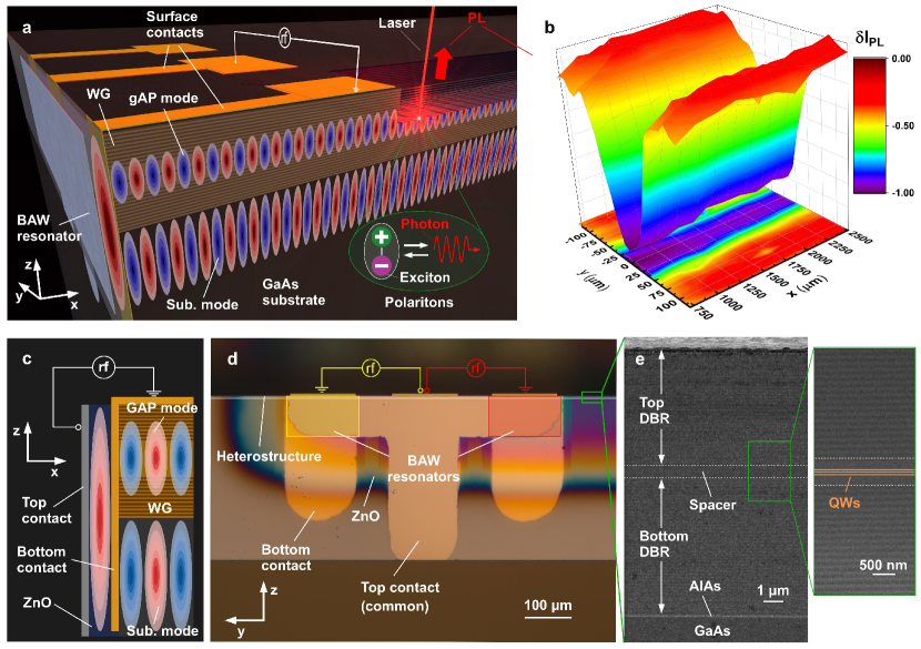
In this paper, we introduce a novel platform for electrically driven optomechanics based on guided bulk acoustic phonons (gAPs) propagating along an in-plane acoustic waveguide (WG) embedding QW emitters (cf. Fig. 1a). The gAPs are longitudinal acoustic BAWs generated (and also detected) by bulk acoustic wave resonators (BAWRs) fabricated on a cleaved facet of the sample (cf. Figs. 1c-d). The WG platform is particularly suited for integration with active optical elements embedded in the spacer region of a semiconductor microcavity, such as QW emitters. Here, the distributed Bragg reflectors (DBRs) around the spacer confine the optical field around the QWs and, simultaneously, act as claddings of the acoustic WG for gAPs. The embedded acoustic WG is terminated by cleaved sample facets: acoustic specular reflections at these surfaces lead to the formation of acoustic cavities both in the WG and in the underlying substrate regions. At low temperatures (10 K), these cavities are characterized by a very high quality factor (), frequency quality factor products () beyond Hz, as well as phonon lifetimes of s at frequencies above 6 GHz. These performance features , which far exceed those so far reported for SAWs and guided BAWs in nanostructures [32, 33]. The gAPs thus combine the in-plane propagation of SAWs and, therefore, their ability to acoustically integrate and interconnect planar structures with the high-frequencies, long coherences, and access to buried structures typical of BAWs.
Furthemore, we also demonstrate the application of the WG platform for GHz optomechanics based on MC polaritons. Polaritons are light-matter composite bosons arising from the strong coupling between QW excitons and photons in a MC, which form Bose-Einstein-like condensates (BECs) at high particle densities [34]. These particles are specially interesting for optomechanics due to the long spatial and, in the BEC state, temporal coherences as well as the strong resonant interactions with phonons mediated by their excitonic component. [29, 8, 35, 36, 37, 38, 39]. The strong overlap of the acoustic and optoelectronic fields in the MC space induces a huge modulation of the strength (>80%) and energies (up to 3 meV) of the polariton resonances, which then become a sensitive local probe of the phonon fields. As an example, Fig. 1b displays a map of the gAP field profile along the MC surface obtained by detecting the phonon-induced changes () of the polariton photoluminescence (PL). The latter shows the highly collimated propagation of gAPs over mm distances along the narrow channel (approx. m-wide) defined by the acoustic beam. Finally, we show that the gAPs and polaritons in the WG coherently couple to acoustic modes in the substrate via piezoelectric backfeeding mediated by the BAWR, which establishes the feasibility of phonon-mediated, interlayer coupling. The embedded WG platform compatible with planar optical MCs thus opens a way for the interconnection of remote on-chip quantum systems and for electrically driven GHz optomechanics using high-quality, active optical systems distributed on a semiconductor chip.
2 Methods
2.1 Polariton-phonon hybrid microcavities
The studies were carried out on an (Al,Ga)As planar MC epitaxially grown on a nominally undoped, GaAs (001) wafer with a thickness of m. The MC spacer embeds ten 15 nm-thick GaAs QWs positioned at antinodes of the optical MC field. It is surrounded by DBRs designed to enable polariton formation via the strong coupling between nm photons (at 10 K) and QW excitons and, simultaneously, act as the core and cladding regions of an acoustic WG sustaining gAPs with frequencies around 6.5 GHz propagating along the direction. Details of the sample design as well as the optical and acoustic properties of the MC layers are summarized in Sec. S1 of the Supplement. The spacer embedding the QWs consists of a 652-nm-thick AlxGa(1-x)As layer stack with an average Al concentration of . It is surrounded by AlGaAs/AlGaAs DBR layer stacks with a high Al composition contrast to increase the optical reflectivity. The average Al composition of the DBRs determines their effective acoustic velocity relative to the WG core and, thus, their acoustic cladding efficiency. The layer structure was designed by appropriately tailoring the thicknesses and Al composition profile of the overlayers to maintain a high optical factor while reducing acoustic leakage from the WG core to the substrate. The final structure has the following layer sequence (from the surface to the interface with the substrate): DBR1/DBR2/spacer/DBR3/DBR4 (see Table S1 for further details). The individual DBR layers have thicknesses equal to either or , where nm is the MC optical resonance wavelength and () the layer refractive index. The top DBR (DBR1) consists of 3 layer pairs with Al concentrations and and thicknesses of 202.89 and 58.82 nm, respectively. DBR2 is composed of 27 pairs with , and thicknesses of 67.63 and 58.82 nm, respectively. DBR3 and DBR4 are comprise of 35 and 3 layer pairs with the same Al concentrations and thicknesses as DBR2 and DBR1, respectively. For further acoustic isolation, an additional 120-nm-thick AlAs layer was inserted between the bottom DBR and the substrate.
Figure 1e displays a scanning electron micrograph of the MC region around the spacer. The individual layers can be identified in the enlarged view in the right panel, where the darker regions correspond to areas with a higher Al concentration.
2.2 BAWR fabrication on cleaved facets
The studies were performed on 3.5 mm-wide and 7 mm-long chips cleaved from the original MC wafer along a direction. BAWs propagating along the MC spacer (gAPs) and the substrate (which will be denoted as substrate modes) were excited by ZnO-based piezoelectric BAWRs placed on the wider (i.e., 7 mm-long) cleaved facet, as illustrated in Figs. 1a and 1d. Acoustic reflections at the cleaved edges leads to the formation of acoustic cavities in both regions with a length of mm corresponding to the chip width. The BAWRs were fabricated using shadow masks to define the areas of the metal contacts and of the piezoeletric ZnO film. The masks were mechanically machined on boron-nitride plates with minimum openings of approximately m. The bottom (top) BAWR contact consists of a 30 nm-thick Au (Al) film deposited on a 10 nm Ti adhesion layer. The textured ZnO films were deposited on the bottom contact via magnetron sputtering at 100∘C. ZnO film thicknesses of 200 and 500 nm yield BAWRs with central resonances frequencies between 5 and 10 GHz, where is the ZnO longitudinal acoustic velocity along the -axis [1]. Results will be presented for BAWRs with a nominal ZnO thickness nm, which yields a resonance band centered at around the RF frequency GHz. Further details of the ZnO sputtering process and BAWR fabrication can be found in Sec. S2.
The optical micrograph of Fig. 1d shows two cleaved facet BAWRs sharing a common top contact. The colored areas are interference fringes associated with variations in the thickness of the ZnO film towards the edges defined by the shadow mask. The BAWR active areas, which correspond to the overlapping region of the top and bottom contacts, have dimensions of m2. Only a very small fraction of this area (of approx. 0.7%) overlaps with the nm-thick MC spacer (cf. Fig. 1e). As a result, the RF power applied to the BAWR excites gAPs along the MC spacer as well as strong BAW modes in the substrate (substrate modes). Finite element simulation studies demonstrating the acoustic excitation of BAWs by the resonators as well as their guiding along the MC spacer region are presented in Sec. S3.
2.3 Optical and radio-frequency spectroscopy
The radio-frequency (RF) and optical spectroscopic studies were performed in a low temperature probe station (10 K) with RF probes to contact the BAWRs as well as optical access for microscopic photoluminescence spectroscopy (PL) with a spatial resolution of approx. m (details of the experimental setup are summarized in Sec. S7). The frequency dependence of the RF-scattering () parameters of the BAWRs was recorded using a vector network analyzer with Fourier transform capabilities. In-situ calibration standards were used to correct for the effects of the cables and probes on the electrical response. The time-domain traces revealing the acoustic echoes were obtained by Fourier transforming the frequency response recorded over a MHz band for different central frequencies. Strickly speeking, these echoes correspond to the delay for refocusing via constructive interferences at the BAWR of the modes excited within the frequency band. In the optical studies, the BAWRs were driven by an RF-generator delivering nominal powers of up to 20 dBm. The PL was excited by either a pulsed laser diode (wavelength nm, pulse width of ps, repetition rate of 40 MHz, and an average fluence mW) or a continuous wave Ti-Sapphire laser operating at wavelengths around 760 nm. The PL spectra were recorded away from the BAWR electrical contacts (distances 500 m) to minimize direct effects of the RF field.
The spectroscopic properties of the MC samples are summarized in Sec. S6. Non-uniformities of the molecular fluxes during the epitaxial growth of the MC induce a small (<2%) reduction of the layer thicknesses as one goes from the center to the border of the GaAs wafer with a diameter of 50.4 mm. The thickness variation primarily affects the MC optical mode, which blue-shifts towards the wafer border. The energetic detuning between the bare optical () MC mode relative to the electron heavy-hole () and electron light-hole () thus change with the distance from the wafer center. The coupling between these modes gives rise to three polariton modes denoted (in increasing order of energy) as the lower (LP), middle (MP), and upper polariton states. Section S6 describes a detailed spatial mapping of the polariton modes, which yields the Rabi splitting as well as the energies of the , , and states as a function of . Table S2 lists these properties for the MC chips used in the optical studies.
3 Results
3.1 Acoustical response
The experimental studies were carried out on mm-wide chips cleaved from the original MC wafer. Acoustic reflections at the cleaved facets of the structure in Fig. 1a lead to the formation of an acoustic cavity for gAPs as well as for the substrate modes. Due to the much larger overlap area with the GaAs substrate, the BAWR electrical frequency response is dominated by the fine comb of longitudinal Fabry-Pérot modes of the cavity created in the substrate region with a frequency spacing MHz (see, for details, Sec. S4). Here, is the round-trip delay and mns-1 the acoustic velocity in the substrate.
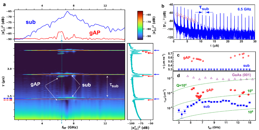
The gAPs modes within the MC spacer can be discriminated from the much stronger substrate modes by recording the echoes in the RF reflection coefficient of the BAWRs using a vector network analyzer with time-domain capabilities (cf. Sec. 2.3). The color map of Fig. 2a shows the frequency dependence of the first few echoes. An echo trace acquired at a central frequency GHz over a long range of delays is displayed in Figure 2b. Here, the most pronounced features are the strong echoes with a round-trip delay , which are indicated by blue arrows in the right panel of Fig. 2a. These echoes are attributed to the substrate modes [cf. Fig. 1d], which can be excited over the whole generation band of the BAWR [up to at least 15 GHz, cf. Fig. 2c].
The large number of echoes (cf. Fig. 2b) enables a precise determination of the BAWR velocity in the substrate region (blue squares in Fig. 2c) as well as of the effective acoustic amplitude absorption coefficient (blue squares in Fig. 2d) [1]. corresponds to the inverse amplitude decay length of the vibrations determined by taking into account losses both during the propagation and reflection at the acoustic WG facets. The BAW amplitudes decay less than 20% over a round trip along the mm-long resonator over the whole frequency range. These decay lengths are thus much longer than those recently reported in Refs. [32] and [1].
The dashed lines in Fig. 2d show the quality factor [1]. Remarkably, the factors for the bulk modes exceed over the whole frequency range leading to products . These values also exceed by more than two orders of magnitude those recently reported for BAW acoustic cavities in GaAs defined by polished (100) surfaces [triangles in Fig. 2d] [1]. The low acoustic absorption is attributed to the high acoustic reflectivity of the cleaved (110) surfaces as compared to the polished ones.
We now turn our attention to the set of weak echoes indicated by the solid red arrows in the right panel of Fig. 2a. In constrast to the substrate echoes, the weak echoes are absent in control samples consisting of a bare GaAs substrate (i.e., without the MC overlayers, cf. Sec. S5). They are attributed to gAP modes confined within the MC structures. The intensity ratio of -23 dB (or 0.5%) between the gAP and bulk echoes compares well with the ratio of approx. 0.6% between the BAWR areas overlapping with the MC spacer and the substrate. In addition, their velocity (, red circles in Fig. 2c) exceeds by approximately 4% the one in the substrate and is thus very close to the one expected for modes tightly confined to the MC spacer (see also Sec. S3). The propagation losses for the gAPs (cf. Figs. 2b (dashed line) and 2d (red circles)) are higher than those for the substrate modes, but their and values still reach the and ranges, respectively.
3.2 Acoustic mode coupling
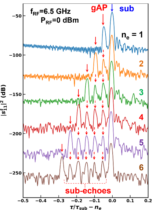
A further remarkable feature in the echo spectra in Fig. 2a (right panel) is the appearance of the sequence of sub-echoes at delays between the bulk and the gAP ones marked by dashed red arrows. A magnified view of the sub-echoes for round-trips is displayed in Fig. 3. The sub-echoes are timely displaced relative to each other (and to the substrate and gAP echoes) by the same delay , where is the round-trip delay of the gAP modes. Moreover, the number of sub-echoes increases after each round trip of the bulk pulse, thus signalizing that each sub-echo corresponds to a new gAP generated after each round trip of the substrate mode. The guided nature of the sub-echoes will be further corroborated by the polariton modulation experiments to be presented in Sec. 3.4.
To address the sub-echo excitation mechanism, we first remind ourselves that a linear coupling between modes in the WG and in the substrate would result in two new modes with well-defined propagation velocities and can, therefore, not account for the delayed appearance of the sub-echoes. Note that the sub-echoes appear in the same narrow frequency range (100 MHz) used to excite the BAWR in the echo experiments. In addition, the well-defined arrival times of the sub-echoes imply that they must be induced by a coherent excitation process, i.e., random scattering events can be discarded as a mechanism for their formation.
The sub-echoes are attributed to the piezoelectric generation of a new gAP pulse each time a substrate echo arrives at the BAWR. In this process, the electric signal generated via the partial absorption of a bulk echo in the substrate region of the BAWR is reconverted to an acoustic signal in the MC region, thus lauching a new gAP pulse in this region. Interestingly, well-defined sub-echoes are only observed in the range of delays for which the gAP echoes are also present. The latter indicates that the piezoelectric generation mechanism may become stimulated in the presence of the gAP mode. We shall see in Sec. 3.4 that the acoustic coupling between acoustic modes in the substrate and in the WG has also an impact on the acoustic modulation of the polariton modes.
3.3 Acousto-optical modulation mechanisms
The optical measurements were carried out at 10 K on a MC with excitons and photons interacting in the strong coupling regime resulting in the formation of polaritons with properties summarized in Sec. S6. We will first consider the phonon modulation mechanisms in a sample with the bare heavy-hole excitonic level () considerably red-shifted with respect to the optical cavity resonance (), i.e., with a cavity-exciton energy detuning meV larger than the vacuum Rabi splitting of meV (sample , cf. Table S2). As will be shown in the following, the large positive detuning simplifies the identification of the exciton-mediated acoustic modulation mechanisms. Results for samples with small detunings and in the lasing regime will be presented in Sec. 3.5.
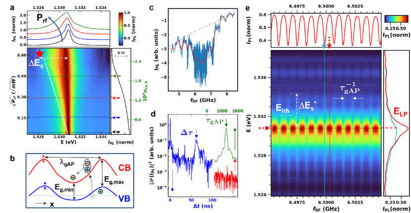
The PL spectrum of sample is dominated by a single line from the lower polariton states ( eV) red-shifted by only one meV with respect to the bare electron heavy-hole exciton level (cf. Fig. 4a, upper panel). For such a large detuning the lower polariton is exciton-like: hence, while the exciton-photon coupling still enhances the optical yield, the acousto-optical coupling becomes primarily determined by the interaction of phonons with the excitonic levels.
The evolution of the time-integrated PL with increasing gAP acoustic amplitude is depicted in the spectral map of Fig. 4a. Here, the gAP amplitude is stated in terms of the square root of the nominal acoustic excitation power . The 2D PL map was generated by normalizing the PL spectrum for each to its maximum intensity to better highlight the changes in line shape. The integrated PL intensity is displayed on the right panel. The PL line broadens with increasing while its intensity reduces. The PL modulation can be understood by assuming the gAP to be a purely longitudinal acoustic standing wave along the direction, i.e., with a strain field consisting of a single component . Here, and denote the gAP wave vector and angular frequency, respectively, and the acoustic wavelength. The strain field modulates the energy of the electron-heavy hole excitonic transition via the deformation potential interaction according to [41]:
| (1) |
where and are the band-gap hydrostatic and the valence band uniaxial deformation potential, respectively. A similar expression with the positive sign replaced by a minus applies to the electron-light hole excitonic transition. In addition to the modulation by the gAP strain field, finite element simulations of the gAP field distribution reveal that the QWs within the MC spacer are also subjected to a small, strain-induced piezoelectric potential (, see Sec. S3). A pure longitudinal strain along does not generate a longitudinal piezoelectric component: the latter arises from the admixture of other strain components arising from the lateral confinement of the WG. This piezoelectric field, though much weaker than those typically found for SAWs [42], can also ionize excitons and, consequently, weaken and broaden excitonic transitions [42]. We have exploited the dependence of the PL intensity on acoustic intensity to map the gAP transport path in Fig. 1b.
The combined effects of the strain and piezoelectric fields yield the time-dependent modulation of the band edges sketched in Fig. 4b. The emission energies oscillate between the minimum () and maximum () modulation amplitudes given by Eq. (1) at strain anti-nodes displaced by m. At each time, the free carriers arising from exciton dissociation by the piezoelectric field tend to drift and accumulate at these regions. The band-gap gradient forces excitons to drift laterally and recombine around the regions of minimum band gap. With increasing , the PL spectra are thus expected to develop the asymmetric shape displayed in Fig. 4a with a pronounced tail toward lower energies, while the position of the high energy flanks remain approximately constant. The strain amplitude can be estimated from the maximum red-shifts indicated by the white line superimposed on the main plot of Fig. 4a. The right axis scale of the right panel yields the corresponding strain amplitudes determined using deformation potentials eV and eV [43].
3.4 Frequency dependence of the PL modulation
While the electrical (rf) echo response probe all modes propagating in the MC overlayers (and substrate), the acousto-optical studies predominantly sample the interaction between polariton and acoustic modes strongly confined around the MC spacer embedding the QWs. The optical experiments can thus directly determine the generation efficiency of these modes as a function of frequency, as displayed in Fig. 4c. The gAPs create a band of pronounced PL quenching centered at 6.5 GHz: this band overlaps well with the emission band for the substrate modes determined by the electrical measurements (, cf. upper panel of Fig. 2a). The strong acousto-optical modulation by gAPs modes with frequencies around 6.5 GHz (cf. Fig. 4c) confirms the electrical excitation of gAPs modes as well as their confinement around the MC spacer. The latter is further supported by the finite element simulations presented in Secs. S3 and S4 (see, in particular, Fig. S1a). Furthermore, the oscillations at the flanks of the excitation band of Fig. 4c are also present in the calculated acousto-electric response for the same mode displayed in Fig. S2. These most likely arise from the interference of different acoustic modes propagating in the overlayers, as can be appreciated in the simulation results of Fig. S1. Finally, the dashed blue line superimposed on Fig. 4c indicates that the degree of PL quenching efficiency increases at low RF frequencies. The latter is attributed to an increased admixture of modes with a large piezoelectric potential at low frequencies (see, for details, Sec. S4).
In contrast to the band around 6.5 GHz, gAPs at higher frequencies (i.e., GHz in Figs. 2c and 2d) are guided modes with fields considerably extending over the DBR cladding layers, as illustrated in Fig. S1b. The echoes corresponding to these modes are too weak to be identified in the color scale of Fig. 2a, in part due to the weak response of the transducer in this frequency range. They can, however, be directly detected in the echo profiles (e.g., the ones delivering the data for Figs. 2c and 2d) as well as in samples with transducers designed for the higher frequency range (see Sec. S6). PL studies in this frequency range revealed, however, a negligible acoustic modulation, a result consistent with a weak acoustic confinement within the MC spacer region. The acousto-optic studies presented here will concentrate on the 6.5 GHz band, where the guided mode profiles strongly overlap with the cavity spacer.
The spectral response in Fig. 4c also displays pronounced short-period oscillations at the center of the emission band (i.e., between 6 ad 7 GHz), which yield information about the gAP dynamics as well as about their interactions with the substrate mode. The time scales associated with these oscillations are revealed in the Fourier power spectrum () displayed in Fig. 4d. The strongest Fourier component corresponds to the round-trip time s of the gAP modes [cf. Fig. 2a], which form a standing acoustic field in the WG cavity. The spatial resolution of the PL measurements does not allow us to resolve the small spatial separation ( nm) between the field antinodes. The individual longitudinal modes of the gAP cavity can nevertheless be accessed via a fine frequency scan, which reveals the frequency comb with periodicity MHz displayed in Fig. 4e. The right panel of this figure compares spectra at a field node and an antinode: note that small changes in frequency have a significant impact on the PL spectrum. More important, the strong strain fields at the comb frequencies induce oscillating energy shifts of the lower polariton line () with amplitudes as high as meV (cf. Figs. 4a and 4e). We note that yields a lower boundary for the amplitude of the bare exciton energy shifts induced by the gAP, since it neglects effects arising from the spatial and temporal coherence of the polariton modes as well as lateral redistribution of the particles in the modulation profile of Fig. 4b.
Finally, the PL power spectrum of Fig. 4d also displays a pronounced peak centered at the time delay ns corresponding to the difference between the round-trip times for the gAP and substrate modes. The PL modulation at the frequency is attributed to the sub-echoes discussed in Sec. 3.2. The appearance of this component in the optical response confirms the gAP nature of the sub-echoes and, thus, the interaction between these and the substrate modes despite the cladding action of the DBRs.
3.5 Acoustic modulation in the lasing regime
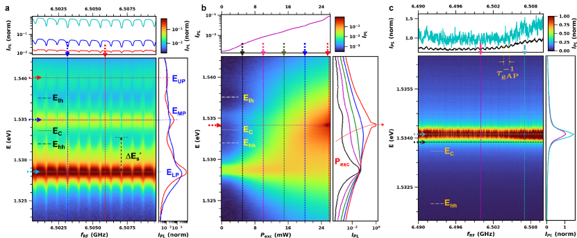
The polariton modulation studies of Sec. 3.3 were carried out on a chip with a large detuning between the bare optical and exciton heavy-hole exciton resonances, which enables direct access to the exciton-mediated process dominating the acousto-optical coupling. We now turn to the small detuning regime, which is more adequate to probe optomechanical features arising from many-body properties (such as lasing and polariton condensation).
Figure 5a displays the dependence of the PL on the gAP excitation frequency recorded on a sample with a detuning meV much smaller than the Rabi splitting meV (sample of Table S2, Sec. S6). The PL map was recorded for low optical excitation density, i.e., in the linear regime, where the emission energies are not affected by shifts due to non-linear polariton interations. At these small detunings, one can detect all three polariton resonances with energies , and resulting from the hybridization of the photonic and excitonic levels.
According to Eq. (1), the deformation potential shifts of the lower polariton level should reduce with the excitonic content of the sample of Fig. 5 (quantified by the Hopfield coefficient , cf. Table S2). Despite the lower excitonic content (of approx. ), the modulation amplitude meV of the lower polariton state in this sample is comparable to the one for the highly excitonic sample of Fig. 4e (). As mentioned in Sec. 3.4, the observed gAP-induced energy shifts depend not only on the excitonic content but also on the spatial coherence and lateral transport properties of the polaritons, which also vary with detuning. In addition, the amplitude of the standing strain field is sensitive to variations in the BAWR transduction efficiency and losses of the acoustic WG may vary from sample to sample. The latter hinder a precise correlation between the detuning and the acoustically induced energy shifts .
The dependence of the polariton levels on the optical excitation power () is displayed in Fig. 5b. The integrated polariton emission intensity grows exponentially with (cf. upper panel). For mW one reaches a lasing regime for mW characterized by a narrow line with spectral width limited by the experimental resolution of the optical setup of approx. 0.25 meV. Furthermore, the lasing mode is considerably blue-shifted (by approximately 5 meV) with respect to the LP polariton emission at low optical excitations. Its energy lies very close to the bare optical resonance (cf. Fig. 5) determined in Sec. S6 ( was determined with an uncertainty of meV) and does not further blue-shifts with increasing excitation density. A similar behavior was also observed for other samples with small detunings (e.g., sample of Table S2).
The polariton PL experiments were performed by using a small laser excitation spot (diameter of approx. 3 m) and by collecting the PL over a wider area over the sample surface. The large energy blueshift is attributed to interactions with the excitonic reservoir created at the laser spot, which then drives a lateral polariton flow via repulsive interactions [44]. The energetically wide polariton emission at high excitation can thus be accounted for by polariton interactions with the spatially inhomogeneous excitonic reservoir.
The proximity of the lasing energy to the bare photonic mode normally points to a photonic rather than to a polariton lasing mechanism. A careful analysis of the PL evolution displayed in the right panel of Fig. 5b indicates, however, that the lasing mode might also have evolved from the broad polariton mode indicated by the arrow in the right panel, which initially blue-shifts with increasing and eventually transitions to a polariton condensate. Based on these considerations, it is not possible to unambiguously establish whether the lasing line in Fig. 5b arises from polariton condensation or from pure photonic lasing.
The acoustic PL modulation in the lasing regime is shown by the spectrum in Fig. 5c. Similarly to the sub-threshold, linear polariton regime, the integrated intensity of the main PL line shows pronounced spectral changes with frequency (cf. cross-sections displayed in the upper and right panels). In contrast to Fig. 5a, however, periodic patterns cannot be clearly identified in the frequency dependence. It is interesting to note that oscillation components at the comb frequency can nevertheless be identified, in particular if one probes the emission at the lower energy flank of the main line, as shown by the black horizontal dashed line in the upper plot. In addition, a modulation component at this frequency also appears in the Fourier power spectrum displayed as a red curve in Fig. 4d. The amplitude of the oscillations are, however, much smaller than those observed in Figs. 4e and 5a. Except for this component, no other ones could be identified in the Fourier analysis.
Finally, we briefly speculate on the reasons for the reduced acoustic modulation in the lasing regime. A transition to pure photonic lasing would naturally reduce contributions from the strong, exciton-related deformation potential (electrostrictive) modulation leaving behind the weaker, photon-related elasto-optic effects (i.e., radiation pressure). In the case of polariton lasing, the smaller acoustic modulation amplitudes as compared to the sub-threshold regime in Fig. 5a cannot be accounted for by a lower exciton content . In fact, due to the large Rabi splitting, the polariton modes at the lasing energy of Fig. 5c still have a significant excitonic fraction despite the large energy blueshift. Rather than , the screening of the strain modulation potential at high particle densities may play the dominating role. As reported for polariton condensates under a SAW,[29, 44] a dynamic polariton redistribution along the wave propagation direction can significantly reduce the effective energy modulation amplitude at high polariton densities. Here, we note that the energy blueshifts caused by polariton-polariton interactions in Fig. 5b exceed the energy modulation amplitudes at low excitation densities (cf. Fig 5a). Polariton redistribution within distances of one acoustic wavelength can, thus, effectively smoothen the acoustic modulation potential.
4 Conclusions
We have introduced a novel platform for electrically driven optomechanics based on the tight confinement of GHz phonons, photons, and excitons in a planar semiconductor MC thus enabling strong interactions among these particles. In this platform, the phonons propagate within a cavity consisting of an embedded waveguide terminated by highly reflective cleaved surfaces. The low acoustic losses of the MC lead to very high quality factors () at frequencies up to several GHz at low temperatures (10 K). The planar geometry enables the on-chip integration and phonon-mediated interconnection of opto-electronic systems, which can be extended to the depth dimension.
The long temporal coherences in the lasing regime open new prospects for non-adiabatic acoustic modulation. As discussed in the previous section, further experimental studies are needed to clarify the modulation processes in this regime. Here, a promissing approach is the investigation of the interaction of gAPs with polaritons confined within -sized intracavity traps in structured microcavities [45, 46, 37, 47]. We anticipate that the fabrication process of these structured MCs is fully compatible with the ones with acoustic WGs studied in this work. Polariton confinement significantly reduces the polariton condensation threshold. In addition, the decoherence rate of confined polariton condensates can reach values GHz much lower than the phonon frequency, thus enabling acoustic modulation in the sideband-resolved regime [37]. Prospects for future studies thus include the coherent GHz modulation of confined polaritons condensates [29] as well as phonon-mediated coupling and interconnection of intracavity polariton traps [45, 48, 46]. The acousto-optical interaction is coherent in the sense that the phonons and polaritons can interchange both amplitude and phase information in a reversible way. The platform thus opens the way for studies of vibration-mediated coherent coupling down to the single-particle level, as well as for novel phonon-based control of active opto-electronic devices.
Funding
This work received support from the European Commission (EU) and German Bundesministerium für Bildung und Forschung (BMBF) (grant EU-QuantERA Interpol/EU-BMBF 13N14783) as well as from the German Deutsche Forschungsgemeinschaft (DFG) (grant 426728819).
Acknowledgments
We thank M. Ramsteiner and M. Yuan for comments and discussions, as well as W. Seidel, S. Rauwerdink, W. Anders, and S. Meister for the help in device processing. We also acknowledge the technical support from R. Baumann on establishing the sample fabrication process.
Disclosures
The authors declare no conflicts of interest.
Data availability
Data underlying the results presented in this paper are not publicly available at this time but may be obtained from the authors upon reasonable request.
Supplemental document
See Supplement for supporting content.
References
- [1] L. Midolo, A. Schliesser, and A. Fiore, “Nano-opto-electro-mechanical systems,” \JournalTitleNature Nanotechnology 13, 11–18 (2018).
- [2] A. H. Safavi-Naeini, D. V. Thourhout, R. Baets, and R. V. Laer, “Controlling phonons and photons at the wavelength scale: integrated photonics meets integrated phononics,” \JournalTitleOptica 6, 213–232 (2019).
- [3] D. A. Golter, T. Oo, M. Amezcua, K. A. Stewart, and H. Wang, “Optomechanical quantum control of a nitrogen-vacancy center in diamond,” \JournalTitlePhys. Rev. Lett. 116, 143602 (2016).
- [4] H. Li, S. A. Tadesse, Q. Liu, and M. Li, “Nanophotonic cavity optomechanics with propagating acoustic waves at frequencies up to 12 GHz,” \JournalTitleOptica 2, 826–831 (2015).
- [5] S. Kapfinger, T. Reichert, S. Lichtmannecker, K. Muller, J. J. Finley, A. Wixforth, M. Kaniber, and H. J. Krenner, “Dynamic acousto-optic control of a strongly coupled photonic molecule,” \JournalTitleNat Commun 6, 8540 (2015).
- [6] S. Hermelin, S. Takada, M. Yamamoto, S. Tarucha, A. D. Wieck, L. Saminadayar, C. Bauerle, and T. Meunier, “Electrons surfing on a sound wave as a platform for quantum optics with flying electrons,” \JournalTitleNature 477, 435–438 (2011).
- [7] R. P. G. McNeil, M. Kataoka, C. J. B. Ford, C. H. W. Barnes, D. Anderson, G. A. C. Jones, I. Farrer, and D. A. Ritchie, “On-demand single-electron transfer between distant quantum dots,” \JournalTitleNature 477, 439–442 (2011).
- [8] A. S. Kuznetsov, D. H. O. Machado, K. Biermann, and P. V. Santos, “Electrically driven microcavity exciton-polariton optomechanics at 20 GHz,” \JournalTitlePhys. Rev. X 11, 021020 (2021). Https://arxiv.org/abs/2003.01051.
- [9] M. Metcalfe, S. M. Carr, A. Muller, G. S. Solomon, and J. Lawall, “Resolved sideband emission of InAs/GaAs quantum dots strained by surface acoustic waves,” \JournalTitlePhys. Rev. Lett. 105, 037401 (2010).
- [10] A. D. O Connell, M. Hofheinz, M. Ansmann, R. C. Bialczak, M. Lenander, E. Lucero, M. Neeley, D. Sank, H. Wang, M. Weides, J. Wenner, J. M. Martinis, and A. N. Cleland, “Quantum ground state and single-phonon control of a mechanical resonator,” \JournalTitleNature 464, 697–703 (2010).
- [11] J. D. Teufel, D. Li, M. S. Allman, K. Cicak, A. J. Sirois, J. D. Whittaker, and R. W. Simmonds, “Circuit cavity electromechanics in the strong-coupling regime,” \JournalTitleNature 471, 204–208 (2011).
- [12] K. J. Satzinger, Y. P. Zhong, H.-S. Chang, G. A. Peairs, A. Bienfait, M.-H. Chou, A. Y. Cleland, C. R. Conner, É. Dumur, J. Grebel, I. Gutierrez, B. H. November, R. G. Povey, S. J. Whiteley, D. D. Awschalom, D. I. Schuster, and A. N. Cleland, “Quantum control of surface acoustic-wave phonons,” \JournalTitleNature 563, 661–665 (2018).
- [13] Y. Chu, P. Kharel, T. Yoon, L. Frunzio, P. T. Rakich, and R. J. Schoelkopf, “Creation and control of multi-phonon fock states in a bulk acoustic-wave resonator,” \JournalTitleNature 563, 666–670 (2018).
- [14] M. V. Gustafsson, T. Aref, A. F. Kockum, M. K. Ekström, G. Johansson, and P. Delsing, “Quantum acoustics: Propagating phonons coupled to a superconducting qubit,” \JournalTitleScience 346, 207 (2014).
- [15] M. J. A. Schuetz, E. M. Kessler, G. Giedke, L. M. K. Vandersypen, M. D. Lukin, and J. I. Cirac, “Universal quantum transducers based on surface acoustic waves,” \JournalTitlePhys. Rev. X 5, 031031 (2015).
- [16] C. C. W. Ruppel, “Acoustic wave filter technology - a review,” \JournalTitleIEEE Trans. Ultrason., Ferroelectr., Freq. Control 64, 1390–1400 (2017).
- [17] Q. Liu, H. Li, and M. Li, “Electromechanical brillouin scattering in integrated optomechanical waveguides,” \JournalTitleOptica 6, 778–785 (2019).
- [18] M. Weiß, S. Kapfinger, T. Reichert, J. J. Finley, A. Wixforth, M. Kaniber, and H. J. Krenner, “Surface acoustic wave regulated single photon emission from a coupled quantum dot–nanocavity system,” \JournalTitleAppl. Phys. Lett. 109, 033105 (2016).
- [19] M. Weiß and H. J. Krenner, “Interfacing quantum emitters with propagating surface acoustic waves,” \JournalTitleJ. Phys. D: Appl. Phys. 51, 373001 (2018).
- [20] A. Hernández-Mínguez, Y.-T. Liou, and P. V. Santos, “Interaction of surface acoustic waves with electronic excitations in graphene,” \JournalTitleJ. Phys. D: Appl. Phys. 51, 383001 (2018).
- [21] H. Tian, J. Liu, B. Dong, J. C. Skehan, M. Zervas, T. J. Kippenberg, and S. A. Bhave, “Hybrid integrated photonics using bulk acoustic resonators,” \JournalTitleNat Commun 11, 3073 (2020).
- [22] D. B. Sohn, S. Kim, and G. Bahl, “Time-reversal symmetry breaking with acoustic pumping of nanophotonic circuits,” \JournalTitleNat. Photonics 12, 91–97 (2018).
- [23] K. C. Balram, M. I. Davanćo, J. D. Song, and K. Srinivasan, “Coherent coupling between radiofrequency, optical and acoustic waves in piezo-optomechanical circuits,” \JournalTitleNat. Photonics 10, 346–352 (2016).
- [24] D. B. Go, M. Z. Atashbar, Z. Ramshani, and H.-C. Chang, “Surface acoustic wave devices for chemical sensing and microfluidics: a review and perspective,” \JournalTitleAnal. Methods 9, 4112–4134 (2017).
- [25] B. Jusserand, A. N. Poddubny, A. V. Poshakinskiy, A. Fainstein, and A. Lemaitre, “Polariton resonances for ultrastrong coupling cavity optomechanics in multiple quantum wells,” \JournalTitlePhys. Rev. Lett. 115, 267402 (2015).
- [26] C. Rocke, S. Zimmermann, A. Wixforth, J. P. Kotthaus, G. Böhm, and G. Weimann, “Acoustically driven storage of light in a quantum well,” \JournalTitlePhys. Rev. Lett. 78, 4099 (1997).
- [27] O. D. D. Couto, Jr., S. Lazić, F. Iikawa, J. Stotz, R. Hey, and P. V. Santos, “Photon anti-bunching in acoustically pumped quantum dots,” \JournalTitleNat. Phot. 3, 645 (2009).
- [28] M. M. de Lima, M. van der Poel, P. V. Santos, and J. M. Hvam, “Phonon-induced polariton superlattices,” \JournalTitlePhys. Rev. Lett. 97, 045501 (2006).
- [29] E. A. Cerda-Méndez, D. N. Krizhanovskii, M. Wouters, R. Bradley, K. Biermann, K. Guda, R. Hey, P. V. Santos, D. Sarkar, and M. S. Skolnick, “Polariton condensation in dynamic acoustic lattices,” \JournalTitlePhys. Rev. Lett. 105, 116402 (2010).
- [30] R. Manenti, M. J. Peterer, A. Nersisyan, E. B. Magnusson, A. Patterson, and P. J. Leek, “Surface acoustic wave resonators in the quantum regime,” \JournalTitlePhys. Rev. B 93, 041411 (2016).
- [31] A. V. Scherbakov, P. J. S. van Capel, A. V. Akimov, J. I. Dijkhuis, D. R. Yakovlev, T. Berstermann, and M. Bayer, “Chirping of an optical transition by an ultrafast acoustic soliton train in a semiconductor quantum well,” \JournalTitlePhys. Rev. Lett. 99, 057402 (2007).
- [32] D. D. Yaremkevich, A. V. Scherbakov, S. M. Kukhtaruk, T. L. Linnik, N. E. Khokhlov, F. Godejohann, O. A. Dyatlova, A. Nadzeyka, D. P. Pattnaik, M. Wang, S. Roy, R. P. Campion, A. W. Rushforth, V. E. Gusev, A. V. Akimov, and M. Bayer, “Protected long-distance guiding of hypersound underneath a nanocorrugated surface,” \JournalTitleACS Nano (2021).
- [33] C. Jean, L. Belliard, T. W. Cornelius, O. Thomas, M. E. Toimil-Molares, M. Cassinelli, L. Becerra, and B. Perrin, “Direct observation of gigahertz coherent guided acoustic phonons in free-standing single copper nanowires,” \JournalTitleJ. Phys. Chem. Lett. 5, 4100–4104 (2014).
- [34] J. Kasprzak, M. Richard, S. Kundermann, A. Baas, P. Jeambrun, J. M. J. Keeling, F. M. Marchetti, M. H. Szymańska, R. André, J. L. Staehli, V. Savona, P. B. Littlewood, B. Deveaud, and L. S. Dang, “Bose-Einstein condensation of exciton polaritons,” \JournalTitleNature 443, 409–414 (2006).
- [35] G. Rozas, A. E. Bruchhausen, A. Fainstein, B. Jusserand, and A. Lemaître, “Polariton path to fully resonant dispersive coupling in optomechanical resonators,” \JournalTitlePhys. Rev. B 90, 201302 (2014).
- [36] J. Restrepo, C. Ciuti, and I. Favero, “Single-polariton optomechanics,” \JournalTitlePhys. Rev. Lett. 112, 013601 (2014).
- [37] D. L. Chafatinos, A. S. Kuznetsov, S. Anguiano, A. E. Bruchhausen, A. A. Reynoso, K. Biermann, P. V. Santos, and A. Fainstein, “Polariton-driven phonon laser,” \JournalTitleNat. Commun. 11, 4552 (2020).
- [38] G. Arregui, N. D. Lanzillotti-Kimura, C. M. Sotomayor-Torres, and P. D. García, “Anderson photon-phonon colocalization in certain random superlattices,” \JournalTitlePhys. Rev. Lett. 122, 043903 (2019).
- [39] A. Fainstein, N. D. Lanzillotti-Kimura, B. Jusserand, and B. Perrin, “Strong optical-mechanical coupling in a vertical GaAs/AlAs microcavity for subterahertz phonons and near-infrared light,” \JournalTitlePhys. Rev. Lett. 110, 037403 (2013).
- [40] D. H. Machado, A. Crespo-Poveda, A. S. Kuznetsov, K. Biermann, L. V. Scalvi, and P. V. Santos, “Generation and propagation of superhigh-frequency bulk acoustic waves in ,” \JournalTitlePhys. Rev. Applied 12, 044013 (2019). ArXiv:1907.09787v2.
- [41] M. M. de Lima, Jr. and P. V. Santos, “Modulation of photonic structures by surface acoustic waves,” \JournalTitleRep. Prog. Phys. 68, 1639 (2005).
- [42] T. Sogawa, P. V. Santos, S. K. Zhang, S. Eshlaghi, A. D. Wieck, and K. H. Ploog, “Dynamic band-structure modulation of quantum wells by surface acoustic waves,” \JournalTitlePhys. Rev. B 63, 121307 (2001).
- [43] O. Madelung, M. Schulz, and H. Weiss, eds., Landolt-Börnstein Tables, vol. 17c (Springer Verlag, Heidelberg, 1984).
- [44] E. A. Cerda-Méndez, D. N. Krizhanovskii, K. Biermann, R. Hey, M. S. Skolnick, and P. V. Santos, “Dynamic exciton-polariton macroscopic coherent phases in a tunable dot lattice,” \JournalTitlePhys. Rev. B 86, R 100301 (2012).
- [45] A. S. Kuznetsov, P. L. J. Helgers, K. Biermann, and P. V. Santos, “Quantum confinement of exciton-polaritons in structured (Al,Ga)As microcavity,” \JournalTitlePhys. Rev. B 97, 195309 (2018).
- [46] A. S. Kuznetsov, K. Biermann, and P. V. Santos, “Dynamic acousto-optical control of confined polariton condensates: From single traps to coupled lattices,” \JournalTitlePhys. Rev. Research 1, 023030 (2019).
- [47] A. S. Kuznetsov, G. Dagvadorj, K. Biermann, M. H. Szymanska, and P. V. Santos, “Dynamically tuned arrays of polariton parametric oscillators,” \JournalTitleOptica 7, 1673–1681 (2020).
- [48] C. Schneider, K. Winkler, M. D. Fraser, M. Kamp, Y. Yamamoto, E. A. Ostrovskaya, and S. Höfling, “Exciton-polariton trapping and potential landscape engineering,” \JournalTitleRep. Prog. Phys. 80, 016503 (2017).
S1 Structural and optical properties of the (Al,Ga)As microcavity
The planar optical microcavity (MC) displayed in Fig. 1 of the main text was grown by molecular beam epitaxy (MBE) on a nominally intrinsic GaAs (001) wafer (Wafer Technology Ltd.). We used a double-side polished substrate with a thickness m, resistivity cm, and Hall mobility (Vs).
The spacer region and the distributed Bragg reflectors (DBRs) of the MC were designed to enhance the coupling between nm photons (at 10 K) and excitons in the embedded GaAs quantum wells (QWs), and, simultaneously, act as the core and cladding regions of the waveguide sustaining guided acoustic phonons (gAPs) propagating along the direction. The layer structure of the MC sample is described in Table S1. The spacer embeds ten 15 nm-wide QWs positioned at antinodes of the optical MC field. Our design uses a nm-thick spacer with an average Al concentration , which yields an average longitudinal acoustic (LA) velocity % higher than in the GaAs substrate, . The spacer thickness sets an upper limit for the acoustic cutoff frequency of the acoustic waveguide equal to GHz. The spacer is surrounced by four types of DBRs with layer thicknesses and Al contents yielding the average velocity profile displayed by the blue dashed line in the right panel of Fig. S1(a). DBR2 and DBR3 consist of stacks of AlGaAs/AlGaAs layers with and , respectively. The layers have optical thicknesses (, defined as the light wavelength in the material) with ratio to ensure a high reflectivity stop-band centered at . The acoustic velocity along these DBRs is approx. 10% higher than in the GaAs substrate.
To further isolate the gAP mode confined around the spacer from the surface and the underlying GaAs substrate, we introduced two additional DBRs (DBR1 and DBR4) with a higher average acoustic velocity (%) around the ones close to the spacer. The Al composition of the individual alloy layers in these DBRs is the same as in DBR2 and DBR3. An overall higher Al concentration was achieved by using DBR stacks with layer thicknesses of , i.e., by increasing the thickness of the DBR layers with the highest Al content. This arrangement makes these DBRs second order Bragg grating for the optical mode. Finally, a 120-nm-thick AlAs was deposited between the bottom DBR4 and the GaAs substrate to further improve the acoustic cladding action.
| Region | d (nm) | (nm) | v(x)/v(GaAs) | |||
|---|---|---|---|---|---|---|
| DBR1 | 775 | 0.73 | 1.134 | 3.16 | ||
| DBR2 | 3378 | 0.55 | 0.15:0.90 | 1.097 | 3.29 | |
| spacer | 652 | 0.23 | 1.037 | 3.50 | ||
| DBR3 | 4379 | 0.55 | 1.097 | 3.29 | ||
| DBR4 | 775 | 0.73 | 1.134 | 3.16 | ||
| AlAs | 120 | 1 | 120 | 1.0 | 1.200 | 3.98 |
| substrate | – | 0 | 0.0 | 1.0 | 3.66 |
S2 Fabrication of the side BAWRs
The bulk acoustic wave resonators (BAWRs) were fabricated by combining photolithographic processing with material deposition through shadow masks. The fabrication of the side BAWRs starts with the deposition of the top contact pads for the side BAWRs consisting of a 40-nm-thick Au film on a 10-nm-thick Ti adhesion layer [cf. Fig. 1(a) of the main text]. Each set of three pads contacts two side BAWRs sharing the central common ground pad. The (001) MC wafer was then cleaved into m2 chips along the and directions of the (001) wafer, respectively, with the highly planar -oriented facet exposing the cross-sections of the top metal pads.
The layers of the BAWR [cf. Fig. 1(d) of the main manuscript] were defined on the facet using shadow masks mechanically machined on boron-nitride plates with minimum openings of approximately m. The bottom contact consists of a 30 nm-thick Au film on a 10-nm-thick Ti adhesion layer evaporated on the cleaved surface. Au was chosen to ensure the rf-magnetron sputtering deposition of textured ZnO films with the hexagonal c-axis aligned along the growth direction, which enhances the piezoelectric properties [1]. Fabrication was finalized with the deposition of the top contact consisting of a 10-nm Ti/30-nm-thick Al/10-nm Ti layers stack.
The rf magnetron sputtering process was carried out in a high-vacuum chamber with a base pressure mbar using a 5-inch-diameter ZnO target placed 6.5 cm above the sample. To ensure the formation of high-resistivity, stoichiometric thin films, we used an oxygen-rich sputtering atmosphere consisting of a Ar/O2 gas mixture (pressure of mbar). The rf sputtering power ( W) and the deposition temperature (C) were chosen to optimize the electro-acoustic performance of the devices while minimizing the density of pinholes [1]. ZnO film thicknesses of 200 and 500 nm yield BAWRs with central resonances frequencies between 5 and 10 GHz, where is the ZnO LA velocity along the -axis.
S3 Propagation of guided modes in microcavities
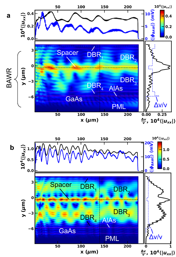
We studied the propagation of modes guided along the MC spacer using finite element (FEM) simulations. The FEM simulations of phonon generation and propagation along the MC were carried out by solving the coupled piezoelectric and mechanical equations using the Gmsh/getDP (http://onelab.info/) software package[2]. In the simulation, an rf input signal of varying frequency was used to excite the side BAWR (cf. Fig. 1 of the main text). The coupled mechanical and piezoelectric equations were then solved in the frequency domain to determine the spatial distribution of the acoustic fields and the total rf converted into acoustic power. The nominal thicknesses of the ZnO layer and the metal BAWR contacts were taken to be equal to the one of the fabricated samples, whereas the thickness of the substrate was set to only one m to reduce the computational efforts. The lateral and bottom sides of the computational domain were surrounded by perfectly-matched layers (PMLs) to avoid acoustic back-reflections. In order to simulate the waveguide performance and minimize the excitation of additional acoustic modes different from the guided mode, the dimension of the BAWR along was made equal to the total thickness of the MC (m).
The color map of Fig. S1(a) is a FEM simulation of the strain profile (corresponding to the uniaxial strain along the gAP direction) of the sample addressed in the main text, which has a BAWR with a nm-thick ZnO layer. The dotted lines delimit the different regions of the sample. The strain profile was determined at the maximum of real part of the admittance () at GHz. The right and upper panel correspond, respectively, to the vertical and horizontal profile of the average strain field across and along the MC spacer (cf. dashed black lines). The dashed blue curve on the right plot displays depth profile of the relative acoustic velocity . The blue curve in the upper plot displays the average piezoelectric potential along the spacer. Away from the BAWR, where it is no longer dominated by near-field effects, the profile develops into a gAP confined around the MC spacer (cf. right panel) and approx. constant amplitude along the WG (cf. black line in the upper panel).
The degree of confinement around the spacer depends on frequency. As an example, we show in Fig. S1(b) the corresponding calculations for the same structure for a mode excited by applying a 10 GHz drive to the same BAWR. Note that in contrast to the 5.8 GHz mode, this mode considerably extends to the DBRs around the spacer, which leads to a higher effective acoustic velocity. In both cases, the rf excitation voltage (equal to Vrms) applied to the BAWR corresponds to a nominal rf power of 10 dBm.
S4 Electrical response of the side BAWRs
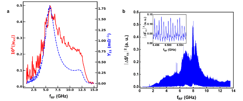
Fig. S2(a) displays the calculated electrical response (the real part of the admittance, ), of the structure of Fig. S1(a). The strain amplitude of the gAP (red line) peaks at the same frequency as the electrical response. Note, however, that the fraction of the electric power coupled to the gAPs increases with frequency. Finally, the calculations also show a non-vanishing piezoelectric potential within the spacer region [blue curve in the upper panel of Fig. S1(a)], which arises from small strain components different from . As discussed in the main text, this potential impacts the optical response.
Fig. S2(b) shows the delayed electrical reflectivity at K of a BAWR with nm. yields the fraction of electric input power converted into a gAP mode, which then bounces back from the opposite cleaved edge of the wafer and is partially reconverted into an electrical signal by the BAWR. It was obtained by Fourier filtering the rf-scattering parameter (corresponding to the electrical reflection) in the time domain to eliminate short-time ( ns) purely electromagnetic response. The spectrum is dominated by the fine comb of Fabry-Pérot modes of high-quality acoustic cavity in the substrate region with a frequency spacing given by MHz (cf. inset), where mns-1 and mm is the cavity length.
S5 Echo spectroscopy
In order to confirm that the extra echo peaks marked by red arrows in Fig. 2(a) of the main text are associated with gAPs, we compared in Fig. S3(a) the echo response of a side BAWR of the MC sample with the one of a control sample on a bare GaAs substrate for GHz at 10 K. Note that the fast echoes due to gAP modes confined along the MC spacer (red arrows) only appear in the MC sample.
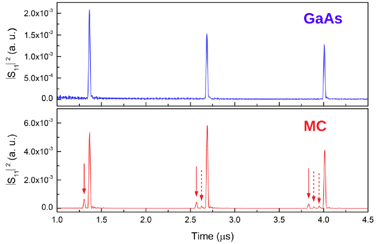
The acousto optical studies presented in the paper show that the weak echoes around 6.5 GHz [cf. Fig. S3 (lower panel)] are associated with acoustic modes strongly confined around the MC spacer. The MC structure also sustains propagating modes extending over the DBRs, as shown by the red symbols between 10 and 15 GHz in Figs. 2c and 2d as well as by the simulation results of Fig. S1: while modes around 6 GHz are confined within the MC spacer, those at higher frequencies (10 GHz) extend considerably into the DBR cladding layers. The weak echoes corresponding to these modes do not appear in the color map of Fig. 2a of the main text, due to its reduced dynamic range as well as the weak response of the transducer in this frequency range. They can, however, be clearly observed in the echo response (cf. Figs. 2c and 2d) as well as in MC samples with transducers designed for a center frequency of 11 GHz by using a thinner ZnO piezoelectric layer (not shown). PL studies on these samples revealed, however, negligible polariton modulation by these modes, which is consistent with a weak confinement within the spacer region. The observation of the weak echoes is, therefore, not a proof of mode confinement within the MC spacer.
S6 Light-matter coupling in the microcavity
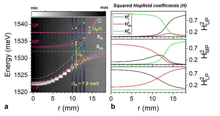
Non-uniformities of the molecular beams during MBE deposition on the 2-inch GaAs substrate surface induce a small (%) reduction of the thickness of the layers from the wafer center () to its border. This thickness gradient induces changes in the energy of the bare (i.e., decoupled) excitonic and photonic states of the MC. PL measurements over the wafer surface enables the determination of the radial () dependence of these energies as well as of the light-matter coupling parameter (the Rabi splitting) describing the interaction between the confined photons and QW excitons in the MC.
The color-coded photoluminescence (PL) map of Fig. S4 displays the optical emission as a function of . The thickness gradient mainly affects the bare (i.e., decoupled from the excitons) optical resonance of the MC, which reaches its maximum value at , while the excitonic modes are weakly thickness dependent. The coupling of the photon field () to the electron-heavy hole () and electron-light hole () excitonic transitions gives rise to three polariton branches denoted as lower (LP), middle (MP), and upper (UP) polariton modes. For large energy negative detunings between the photon and hh transitions, the UP mode is very week and cannot be detected in the plot. The two resonances at are attributed to the lower and middle polariton modes with strongly photonic and hh excitonic characters, respectively. The bare photonic energy increases with increasing and, eventually, anti-crosses the bare excitonic resonances.
In order to extract the bare photon () and exciton energies ( and ), we neglected the small dependence of the bare excitonic resonances on thickness and assumed a quadratic dependence of photonic energies on according to
| (S1) |
We then fit the experimental data in Fig. S3(a) to a coupled oscillator model taking into account the coupling of the electron-heavy hole and electron-light hole excitonic transitions with a position dependent photon resonance expressed by the following Hamiltonian in the basis of states :
| (S2) |
Here, is the Rabi splitting between the photonic and heavy hole excitons. The corresponding coupling for the light-hole states was assumed to be three times smaller, in agreement with ratio between the oscillator strengths for lh and hh transitions.
The eigenvalues and eigenvectors of yield the LP, MP, and UP polariton branches as well as the Hopfield coefficients () for the three branches as a function of the parameters , , , and . The purple lines in Fig. S4a are fits of the eigenvalues of to the measured LP, MP, and UP polariton energies, from which we extracted the bare resonance energies displayed by dashed lines on the same plot as well as a Rabi splitting energy meV. The latter is approximately equal to the minimum energy separation between the LP and MP branches at the zero photon-exciton detuning at mm. Figure S4b displays the radial dependence of the Hopfield coefficients () for the three polariton branches.
The properties of the polariton samples investigated in the present work are summarized in Table S2. is from a region around mm, where the lower polaritons have a strong () excitonic character. While the coupling to photons enhances the optical emission probability, the lowest energy emission lines in the present sample are essentially excitonic (i.e., with a small polaritonic character). This sample has been employed to yield information about the exciton-related BAW modulation mechanisms. The other two samples have detunings close to zero and were used in the modulation experiments in the lasing regimve.
| Sample | r | ||||||
|---|---|---|---|---|---|---|---|
| (mm) | (eV) | (eV) | (eV) | (meV) | (eV) | ||
| 17 | 1.532 | 1.5376 | 1.5432 | 1.5309 | 0.91 | ||
| 12 | 1.532 | 1.5376 | 1.5336 | 1.5289 | 0.58 | ||
| 11 | 1.532 | 1.5376 | 1.5320 | 1.5282 | 0.48 |
S7 Experimental system
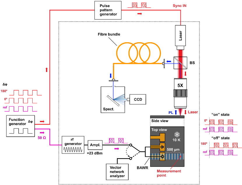
Fig. S5 shows a schematic diagram of the experimental setup. The experiments are carried out in a low temperature probe station at 10 K. The rf signal exciting the BAWRs is generated by an RF signal generator followed by a dBm RF amplifier. For the measurements of the scattering () parameters, the BAWRs are connected to a vector network analyzer. For the optical modulation experiments (region of the setup enclosed by the dashed black square), a cw Ti-Sapphire laser operating at 760.757 nm is focused on the projected acoustic path on the sample surface. The PL spectra are recorded at least m away from the metal pads to minimize direct effects of the rf field on the photoluminescence. The PL signal is collected by a microscope objective and guided to the spectrometer using a fibre bundle, where it is detected by a charged coupled device (CCD) camera.
In the differential PL experiments (PL), we use the whole set up depicted in Fig. S5. The PL is excited by a pulsed laser diode operating at 635 nm (pulse width ps and repetition rate 40 MHz). The signal triggering the laser (synchronization signal, in red), which is generated by a pulse pattern generator, as well as the rf signal driving the BAWR (reference signal, in magenta) are modulated in amplitude by a square wave generated by a function generator with a frequency of a few hundreds of Hz. During the measurements, the phase difference between the two signals is varied between (equivalent to “rf on” state) and (equivalent to “rf off” state). Since the thermal response times are much longer than the modulation frequency, the PL in the “rf on” and “rf off” states are recorded at the same temperature. By doing so, we discriminate the acoustic effects from heating effects induced by the rf applied field.
References
- [1] D. H. Machado, A. Crespo-Poveda, A. S. Kuznetsov, K. Biermann, L. V. Scalvi, and P. V. Santos, “Generation and propagation of superhigh-frequency bulk acoustic waves in ,” \JournalTitlePhys. Rev. Applied 12, 044013 (2019).
- [2] C. Geuzaine, “GetDP: a general finite-element solver for the de Rham complex,” in PAMM Volume 7 Issue 1. Special Issue: Sixth International Congress on Industrial Applied Mathematics (ICIAM07) and GAMM Annual Meeting, Zürich 2007, vol. 7 (Wiley, 2008), pp. 1010603–1010604.