High operating temperature plasmonic infrared detectors
Abstract
III-V semiconductor type-II superlattices (T2SLs) are a promising material system with the potential to significantly reduce the dark current of, and thus realize high-performance in, infrared photodetectors at elevated temperatures. However, T2SLs have struggled to meet the performance metrics set by the longstanding infrared detector material of choice, HgCdTe. Recently, epitaxial plasmonic detector architectures have demonstrated T2SL detector performance comparable to HgCdTe in the 77 K - 195 K temperature range. Here we demonstrate a high operating temperature plasmonic T2SL detector architecture with high-performance operation at temperatures accessible with two-stage thermoelectric coolers. Specifically, we demonstrate long-wave infrared plasmonic detectors operating at temperatures as high as 230 K while maintaining dark currents below the “Rule 07” heuristic. At a detector operating temperature of 230 K, we realize 22.8% external quantum efficiency in a detector absorber only 372 nm thick () with peak specific detectivity of at , well above commercial detectors at the same operating temperature.
The performance of infrared photodetectors, particularly at long wavelengths, degrades drastically with increasing temperature. Often, expensive and bulky cryo-cooling modules are required to reduce detector dark current and maintain acceptable detector performance. In the long-wave infrared (LWIR ), detectors must typically be cooled to near liquid nitrogen temperatures in order to achieve reasonable performance metrics, increasing both the cost and weight of infrared sensor systems. The current and long-time state-of-the-art LWIR detector is the HgCdTe (MCT) photodetector. MCT detectors, in addition to suffering the same high-temperature challenges as any LWIR detector, rely on the epitaxial growth of II-VI alloys, for which uniform growth is notoriously difficult, especially for the high Hg-content HgCdTe alloys required for LWIR detectionRogalski et al. (2019). Moreover, MCT materials are facing increased restrictions, including being banned in European markets, due to environmental concerns associated with mercury and cadmium EUD (2011). For this reason there has been historical, and increasing, interest in developing alternative materials and architectures, specifically in the III-V semiconductor family, for LWIR detectionSchneider and Liu (2007); Rogalski et al. (2019).
Type-II superlattices (T2SLs) comprising III-V semiconductor materials offer a promising alternative to the long-dominant MCT material system for infrared detector applications Smith and Mailhiot (1987); Grein et al. (1992). Specifically, when compared to the MCT material system, T2SLs are less environmentally problematic, offer more uniform growth (due to the lower vapor pressure of III-V materials), leverage mature III-V semiconductor device fabrication processes, and have been theorized to have significantly lower dark currentsGrein et al. (1992). However, T2SL detectors have struggled to meet predicted performance metrics, in part a result of short minority carrier lifetimes Connelly et al. (2010) and/or low absorption coefficients Vurgaftman et al. (2016). One increasingly attractive approach to overcoming the poorer performance of T2SL-based detectors has been to leverage detector architectures which enhance the optical fields in the detector Nolde et al. (2015); Goldflam et al. (2016); Nolde et al. (2019); Canedy et al. (2019); Letka et al. (2019); Nordin et al. (2020a); Kamboj et al. (2021); Nordin et al. (2021a); Letka et al. (2020) to increase detector absorption while maintaining small detector volumes, and therefore low dark currents.
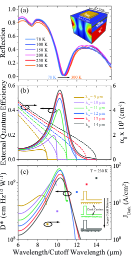
A particularly successful implementation of optically-enhanced T2SL detectors is the recently-demonstrated ultra-thin () plasmonic detectorNordin et al. (2021a), which realizes responsivities commensurate with much thicker traditional detectors (), while also demonstrating dark currents substantially below “Rule 07”Tennant et al. (2008), the heuristic for HgCdTe detectors and thus a useful benchmark for competing detector technologies. In such an architecture, an ultra-thin () T2SL detector structure is grown upon a heavily () doped semiconductor ‘ground-plane’. The interface between this (plasmonic) semiconductor material Law et al. (2012, 2013) and the (dielectric) detector supports surface plasmon-polariton (SPP) modes at LWIR wavelengths. Incident light is coupled into the tightly-bound SPP modes via a patterned 2D grating on the detector surface (Fig. 1(a) inset). The tight confinement of these SPP modes allows for the absorber thickness, and thus dark current, to be drastically reduced.
For the ultra-thin plasmonic detectors, the spectral position of the resonant plasmonic mode (for a given 2D grating geometry and detector thickness) is largely temperature-invariant [Fig. 1(a)], while the effective bandgap of the T2SL decreases with increasing temperature. Figure 1(b) shows rigorous coupled wave analysisFro (RCWA) simulations of plasmonic detector external quantum efficiency (EQE) for absorber cutoff wavelengths from to . For these simulations, we use a complex uniaxial permittivity tensor for the T2SL Gautam et al. (2012) with obtained from our previous workNordin et al. (2021a) and . As can be seen in Fig. 1(b), the simulated absorption (EQE) rapidly increases as the cutoff of the absorber sweeps into the spectral position of the plasmonic mode, after which the absorption (EQE) saturates as the cutoff of extends past the plasmonic mode. Thus, for a detector with excellent low temperature performance, increasing the detector operating temperature offers little additional benefit to responsivity while incurring dramatic increases in dark current [Fig. 1(c)], resulting in significant degradation of detector specific detectivity (). However, if the effective bandgap of the absorber is tailored to extend, at elevated temperatures (T > 200 K), to the spectral position of the plasmonic mode (as opposed to well-past this position on the low-energy side), one would expect to be able to realize the superior performance of the ultra-thin plasmonic T2SL detector, but at significantly elevated temperatures.
Here we demonstrate the flexibility of the plasmonic T2SL detector architecture and, most importantly, the potential for plasmonic T2SL detectors to out-perform commercial near-room temperature thermoelectrically cooled HgCdTe detectors. We achieve a substantial operating temperature and performance increase in the plasmonic detectors, relative to the initial demonstration of these devicesNordin et al. (2021a), by co-designing the optical and electronic structure of the detector architecture. Optically, we leverage the relative temperature invariance of the plasmonic mode. Electronically, we replace the barrier superlattice with a wider bandgap ternary layer of AlAs0.1Sb0.9 to reduce thermionic emission dark current, adjust the absorber superlattice geometry for appropriate cutoff wavelength at high temperatures, and reduce the barrier layer thickness while increasing the absorber layer thickness to maximize EQE and minimize detector turn-on voltage. A detailed description of these adjustments and the detector design evolution is provided in the Supplemental Material. We characterize our detector’s electrical and optical response and compare the results to the “Rule 07” heuristic and commercial MCT detectors. Our detector, operated at 230 K, achieves external quantum efficiency as high as 22.8% in only a 372 nm thickness absorber with dark currents lower than “Rule 07”, a factor of two better than our initial implementationNordin et al. (2021a), resulting in a peak specific detectivity of at . Our plasmonic detector’s specific detectivity is nearly an order of magnitude higher than commercial HgCdTe detectors operating at the same high temperature (230 K). The high operating temperature (HOT) plasmonic detector presented in this work thus offers a viable alternative to environmentally-problematic thermoelectrically cooled HgCdTe.
The detectors are grown on an n-type doped GaSb substrate by molecular beam epitaxy in a Varian Gen-II system with effusion sources for gallium, indium, aluminum, and silicon, and valved cracker sources for arsenic and antimony. Growth begins with a Te doped (n-type ) GaSb buffer, above which is grown the plasmonic virtual substrate, comprising 123 periods of Si doped mid-wave infrared (MWIR) InAs/InAs0.49Sb0.51 T2SL, with each period having 16.5 ML of InAs and 3.5 ML of InAs0.49Sb0.51. Following this plasmonic virtual substrate, the detector structure is grown, beginning with 47 periods of the unintentionally doped (UID) absorber superlattice, with each period having 21.4 ML of InAs and 4.6 ML of InAs0.49Sb0.51. Above the absorber superlattice, 80 nm of ternary AlAs0.1Sb0.9 (UID) is grown, which acts as a barrier layer. We then grow 7 periods of the contact layer T2SL (UID), which has the same composition as the absorber T2SL. The plasmonic layer is grown with a doping concentration of , and corresponding Drude parametersLaw et al. (2012) of a plasma wavelength () and a rad/s scattering rate ( rad/s). Note that while we use a T2SL as our plasmonic layer to simplify lattice-matching to the layers above and below the plasmonic film, the higher energy bandgap of the n++ T2SL, combined with state-filling resulting from the high doping, allows this layer to simply be treated as a Drude metalNordin et al. (2020b, 2021a); Kamboj et al. (2021).
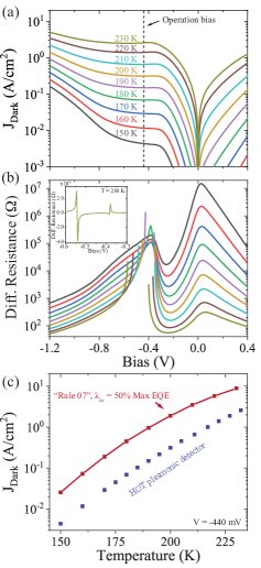
Following epitaxial growth, the as-grown material is patterned into mesas of dimensions x using UV photolithography and a wet etch. The mesas are etched to a depth of 750 nm in order to provide electrical isolation between mesa top contacts. The detector top and bottom contacts, as well as the 2D metal gratings are then defined using UV photolithography and a metallization and lift-off process. The metal layer stack is 3 nm of Pd, 50 nm of Ti, 50 nm of Pt, and 100 nm of Au, which is a standard shallow contact for narrow bandgap T2SL materials. Detectors are left unpassivated, however following lift-off the detectors are thoroughly cleaned in a bath of 90 °C AZ KWIKSTRIP followed by sonication in organic solvents (acetone, methanol, and isopropyl alcohol). For the HOT plasmonic detectors presented here, we use a 2D grating array with a period of and a 50% duty cycle designed to couple incident LWIR light to SPP modes bound to the /T2SL absorber interface. Following fabrication, detectors were mounted onto leadless chip carriers in a custom-designed temperature-controlled cryostat. Dark current measurements were taken with the detector blocked by a copper cold shield thermally connected to the cryostat cold-finger. Temperature dependent detector dark current as a function of applied bias (J-V) was measured using a Keithley 2460 low-noise source-meter and is shown in Figure 2(a).
From -300 mV to -600 mV the JV curves are effectively flat, suggesting a diffusion-limited dark current mechanism. Beyond -600 mV, the dark current is relatively temperature insensitive, suggesting the majority of the additional dark current at high biases is due to band-to-band tunnelling and/or mid-gap carrier generation. Shown in Fig. 2(b) is the temperature dependent differential resistance. For elevated temperatures (TK), we observe clear negative differential resistance (NDR) at the onset of diffusion limited behavior. NDR in photodetectors has been analytically describedWhite (1986, 1987) and observed in HgCdTe detectorsAshley and Elliott (1985) and MWIR III-V detectors Ashley and Elliott (1991), and has traditionally been attributed to depletion and therefore substantial Auger suppression in the detector’s absorber. Given the ultra-thin absorber utilized in the plasmonic detectors, the experimentally-observed NDR in our device could be attributed to a similar depletion mechanism and a commensurate Auger suppression. Shown in Fig. 2(c) is temperature dependent dark current at a bias -440 mV compared to a “Rule 07” where cutoff wavelength at each temperature is determined by the spectral position of 50% of max EQE at that temperature For all temperatures the plasmonic detector shows dark current well below “Rule 07”. Specifically, at 230 K the HOT plasmonic detector possess a dark current lower than “Rule 07”.
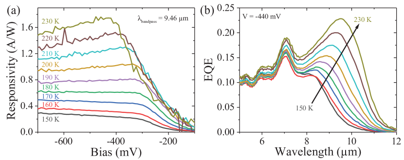
The fabricated detector responsivity was measured using a calibrated blackbody source; details of the measurement and spectral response measurements are described in previous workNordin et al. (2021a). Shown in Fig. 3(a) is the bias-dependent responsivity as a function of temperature. As anticipated for barrier detectors, the responsivity peaks at the onset of diffusion-limited behavior we observe in Fig. 2(a) (relatively flat J-V). However, this saturation occurs at relatively high biases, near -300 mV at low temperatures and as high as -440 mV at 230 K, suggesting the valence band offset between the barrier and the T2SL is nonzero. Future iterations of these devices could lower this turn-on bias by implementing an optimized barrier layer. Additionally, the responsivity increases significantly at elevated temperatures, which is expected behavior resulting from the detector absorber’s cutoff wavelength redshifting into the plasmonic mode and thus enabling the enhanced absorption of SPPs by the detector’s absorber. However, to confirm this anticipated behavior, we need the detector’s EQE spectrum to accurately compare to the simulations show in Fig. 1(b). Shown in Fig. 3(b) is the measured EQE as a function of temperature at -440 mV. As expected, the EQE increases substantially as the detector cutoff redshifts into the plasmonic mode hosted at the /T2SL absorber interface. The substantial increase, and then relative saturation, in EQE that we observe in our devices is nearly identical to the simulated EQE in Fig. 1(b), especially for the (yellow) to (green) lines. However, we do not reach the nearly 50% EQE in Fig. 1(b) for the simulated or detectors, suggesting that the cutoff wavelength of the present detectors could be made slightly longer at 230 K and the increase in EQE may balance the additional dark current. An additional feature at is present, and we attribute this feature to a TE-polarized guided-mode-resonance. Our 2D simulations in Fig. 1(b) do not include this feature because they only consider the (in-plane) TM-polarized absorption.
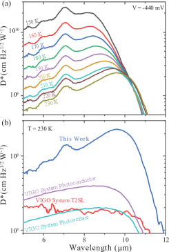
We estimate specific detectivity with the expression , using the measured detector dark current and responsivity (), with the mesa area, the electronic charge, Boltzmann’s constant , the detector temperature, and the differential resistance. The temperature-dependent estimated spectral specific detectivity at a bias of -440 mV is shown in Fig. 4(a). Between 150 K and 230 K the peak specific detectivity only decreases by an order of magnitude. Above 230 K the low-noise preamplifier (SRS 570) used for responsivity and spectral response measurements overloads, so we cannot provide estimated specific detectivity for these higher temperatures. Note that unlike the simulations presented in Fig. 1(c), the experimentally-obtained estimated peak decreases monotonically with temperature. The simulations in Fig. 1(c) show at a fixed temperature for changing cut-off wavelengths (different superlattices). Our experimental results are sweeping both cutoff wavelength and temperature, the latter of which accounts for the additional, and unavoidable, decrease in . We attribute the relatively small reduction in specific detectivity to the exponentially increasing dark current being partially compensated by the increasing EQE as the absorber band edge moves through the optical resonance of the device. To put the current work in context, we compare the results from our HOT plasmonic detector to commercial detectors by plotting our estimated specific detectivity against VIGO system’s thermoelectrically cooled (230 K) MCT detectorsVIG (a, b), both photoconductive and photovoltaic, and VIGO System’s new line of thermoelectrically cooled (230 K) photoconductive T2SL detectorsVIG (c). The HOT plasmonic detector presented in this work shows peak specific detectivities of at 230 K, while the commercial detectors only achieve specific detectivities of to .
The plasmonic LWIR detectors show high performance when the absorber cut-off wavelength sits just beyond the wavelength of the plasmonic resonance, but performance degrades quickly with increasing temperature due to increasing dark current resulting from the decrease in the absorber bandgap. The substantial design flexibility offered by the use of designer epitaxial metals and quantum-engineered device active regions allows for the careful tailoring of the absorber for strongly-enhanced LWIR detection at a given temperature. Specifically, by engineering the electronic and optical structure of our plasmonic detectors, we realize a LWIR detector, operating at 230 K, which out-performs commercial detectors at the same temperature. Moreover, we do so in a III-V material system, which benefits from a mature and well-established semiconductor fabrication and processing infrastructure, and which does not suffer from the environmental concerns and restrictions associated with the HgCdTe alloys. Although these results are a major leap forward in LWIR detector development, there is still a real need to push the operation of high performance infrared detectors to room temperature. A further increase in the operation temperature of the ultra-thin plasmonic detectors will likely require leveraging Auger suppression techniques, perhaps via carefully engineered superlattices Meyer et al. (1995); Muhowski et al. (2020) and/or by implementing novel electronic device architecturesWhite (1986); Lee et al. (2020). The demonstrated detectors highlight only one of a range of optical designs incorporating integrated plasmonic layers. There exists considerable potential for LWIR detector architectures with enhanced functionality, such as ultra-fast detection, or spectrally tunable/switchable detection which could be enabled by different plasmonic optoelectronic architectures Nordin et al. (2021b). The detectors demonstrated here are thus an important step towards room temperature devices, as well as device architectures with the potential to extend the limits of LWIR detection and detector functionality.
In summary, we demonstrate a HOT long-wavelength infrared detector plasmonic detector which out-performs commercial HgCdTe detectors. We achieve this superior performance by carefully tailoring the optical and electronic band structure of our detector for enhanced LWIR absorption at elevated temperatures. The plasmonic detectors at 230 K possess EQEs of 22.8% with dark currents lower than “Rule 07”, and thus peak specific detectivity of . The peak specific detectivity achieved by the plasmonic detectors is nearly an order of magnitude larger that that of commercial MCT detectors operated at the same temperature. The work presented here demonstrates that not only are the plasmonic T2SL detectors a viable replacement for single-element HgCdTe detectors, but in fact out-perform these state-of-the-art commercial detectors on the key figures of merit for detector performance.
Supplementary Material
See the supplementary material for x-ray diffraction measurements of as-grown device material.
Acknowledgements.
DW and LN gratefully acknowledge support from the National Science Foundation (ECCS-1926187). This work was performed in part at the University of Texas Microelectronics Research Center, a member of the National Nanotechnology Coordinated Infrastructure (NNCI), which is supported by the National Science Foundation (grant ECCS-2025227).Data Availability
The data that support the findings of this study are available from the corresponding author upon reasonable request.
References
- Rogalski et al. (2019) A. Rogalski, P. Martyniuk, and M. Kopytko, Progress in Quantum Electronics 68 (2019).
- EUD (2011) Directive 2011/65/EU of The European Parliament and of the Council of 8 June 2011 on the restriction of the use of certain hazardous substances in electrical and electronic equipment, Vol. L174 (2011).
- Schneider and Liu (2007) H. Schneider and H. C. Liu, Quantum well infrared photodetectors (Springer, 2007).
- Smith and Mailhiot (1987) D. L. Smith and C. Mailhiot, J. Appl. Phys. 62, 2545 (1987).
- Grein et al. (1992) C. H. Grein, P. M. Young, and H. Ehrenreich, Appl. Phys. Lett. 61, 2905 (1992).
- Connelly et al. (2010) B. C. Connelly, G. D. Metcalfe, H. Shen, and M. Wraback, Appl. Phys. Lett. 97, 251117 (2010).
- Vurgaftman et al. (2016) I. Vurgaftman, G. Belenky, Y. Lin, D. Donetsky, L. Shterengas, G. Kipshidze, W. L. Sarney, and S. P. Svensson, Appl. Phys. Lett. 108 (2016).
- Nolde et al. (2015) J. A. Nolde, M. Kim, C. S. Kim, E. M. Jackson, C. T. Ellis, J. Abell, O. J. Glembocki, C. L. Canedy, J. G. Tischler, I. Vurgaftman, J. R. Meyer, and E. H. Aifer, Applied Physics Letters 106, 261109 (2015).
- Goldflam et al. (2016) M. D. Goldflam, E. A. Kadlec, B. V. Olson, J. F. Klem, S. D. Hawkins, S. Parameswaran, W. T. Coon, G. A. Keeler, T. R. Fortune, A. Tauke-Pedretti, J. R. Wendt, E. A. Shaner, P. S. Davids, J. K. Kim, and D. W. Peters, Appl. Phys. Lett. 109, 251103 (2016).
- Nolde et al. (2019) J. A. Nolde, E. M. Jackson, M. Kim, C. S. Kim, C. L. Canedy, M. V. Warren, S. Tomasulo, C. A. Affouda, E. R. Cleveland, I. Vurgaftman, J. R. Meyer, and E. H. Aifer, Journal of Nanophotonics 13, 1 (2019).
- Canedy et al. (2019) C. L. Canedy, W. W. Bewley, C. D. Merritt, C. S. Kim, M. Kim, M. V. Warren, E. M. Jackson, J. A. Nolde, C. A. Affouda, E. H. Aifer, I. Vurgaftman, and J. R. Meyer, Opt. Express 27, 3771 (2019).
- Letka et al. (2019) V. Letka, A. Bainbridge, A. P. Craig, F. Al-Saymari, and A. R. J. Marshall, Opt. Express 27, 23970 (2019).
- Nordin et al. (2020a) L. Nordin, A. Kamboj, P. Petluru, E. Shaner, and D. Wasserman, ACS Photonics 7, 1950 (2020a).
- Kamboj et al. (2021) A. Kamboj, L. Nordin, P. Petluru, A. J. Muhowski, D. N. Woolf, and D. Wasserman, Applied Physics Letters 118, 201102 (2021).
- Nordin et al. (2021a) L. Nordin, P. Petluru, A. Kamboj, A. J. Muhowski, and D. Wasserman, Optica 8 (2021a), 10.1364/optica.438039.
- Letka et al. (2020) V. Letka, A. P. Craig, A. Bainbridge, and A. R. J. Marshall, Applied Physics Letters 117, 073503 (2020).
- Tennant et al. (2008) W. E. Tennant, D. Lee, M. Zandian, E. Piquette, and M. Carmody, Journal of Electronic Materials 37 (2008), 10.1007/s11664-008-0426-3.
- Law et al. (2012) S. Law, D. C. Adams, A. M. Taylor, and D. Wasserman, Opt. Express 20, 12155 (2012).
- Law et al. (2013) S. Law, L. Yu, and D. Wasserman, Journal of Vacuum Science & Technology B, Nanotechnology and Microelectronics: Materials, Processing, Measurement, and Phenomena 31 (2013), 10.1116/1.4797487.
- (20) From V. A. Podolskiy’s research group, see https://faculty.uml.edu/vpodolskiy/codes/index.html RCWA for an implementation of Rigorous Coupled Wave Analysis .
- Gautam et al. (2012) N. Gautam, A. Barve, and S. Krishna, Applied Physics Letters 101 (2012), 10.1063/1.4767358.
- Nordin et al. (2020b) L. Nordin, A. Kamboj, P. Petluru, E. Shaner, and D. Wasserman, ACS Photonics 7, 1950 (2020b).
- White (1986) A. M. White, Infrared Physics 26 (1986), 10.1016/0020-0891(86)90009-6.
- White (1987) A. M. White, Infrared Physics 27 (1987), 10.1016/0020-0891(87)90030-3.
- Ashley and Elliott (1985) T. Ashley and C. T. Elliott, Electronics Letters 21 (1985), 10.1049/el:19850321.
- Ashley and Elliott (1991) T. Ashley and C. T. Elliott, Semiconductor Science and Technology 6 (1991), 10.1088/0268-1242/6/12C/020.
- VIG (a) “Vigo system. pc-2te-10.6,” https://vigo.com.pl/en/products_en/pc-2te-10-6/ (a), date accessed: 2021-10-08.
- VIG (b) “Vigo system. pv-2te-10.6,” https://vigo.com.pl/en/products_en/pv-2te-10-6/ (b), date accessed: 2021-10-08.
- VIG (c) “Vigo system. pcas-2te-11-0.1×0.1-to8-wznsear-70,” https://vigo.com.pl/en/products_en/pcas-2te-11-0-1x0-1-to8-wznsear-70/ (c), date accessed: 2021-12-29.
- Meyer et al. (1995) J. R. Meyer, C. A. Hoffman, F. J. Bartoli, and L. R. Ram-Mohan, Appl. Phys. Lett 67, 757 (1995).
- Muhowski et al. (2020) A. J. Muhowski, A. M. Muellerleile, J. T. Olesberg, and J. P. Prineas, Applied Physics Letters 117, 061101 (2020).
- Lee et al. (2020) D. Lee, P. Dreiske, J. Ellsworth, R. Cottier, A. Chen, S. Tallaricao, A. Yulius, M. Carmody, E. Piquette, M. Zandian, and S. Douglas, in Infrared Technology and Applications XLVI, Vol. 11407, edited by B. F. Andresen, G. F. Fulop, J. L. Miller, and L. Zheng, International Society for Optics and Photonics (SPIE, 2020) pp. 93 – 105.
- Nordin et al. (2021b) L. Nordin, P. Petluru, A. J. Muhowski, E. A. Shaner, and D. Wasserman, Journal of Applied Physics 129, 113102 (2021b).