Very large SiPM arrays with aggregated output
Abstract
In this work we will document the design and the performances of a SiPM-based photo-detector with a surface area of conceived to operate as a replacement for PMTs. The signals from SiPMs are summed up to produce an aggregated output that exhibits in liquid nitrogen a dark count rate (DCR) lower than over the entire surface, a signal to noise ratio better than 13, and a timing resolution better than . The module feeds about at with a dynamic range in excess of photo-electrons on a differential line. The unit is compatible with operations at room temperature, with a DCR increased by about orders of magnitude.
1 Introduction
Very large scale experiments are being studied or under construction to unlock the fundamental properties of our universe. Experiments such as Dune, DarkSide, XenonNT, and Darwin share the requirement of detecting faint pulses of light with many photo-sensors capable of operating in cryogenic environment [1, 2, 3, 4].
In the past [5], we demonstrated that it is possible to tile large SiPMs to build a photo-detector working in liquid nitrogen/argon with unprecedented performances. In this work we present a photo-detector with all the auxiliary electronic components required for installation in a particle detector.
2 SiPMs
In this work NUV-HD-Cryo SiPMs from FBK have been used; these devices represent an evolution from [6] in terms of stability at cryogenic temperature. This allows for higher cell size and lower quenching resistance with respect to the NUV-HD-LF devices used in [5, 7]. An overview of the SiPM electrical parameters is reported in Table 1. The performances of NUV-HD-Cryo SiPMs have been reported in [8, 9, 10]: in liquid nitrogen, the Dark Count Rate (DCR) is lower than at with a negligible after-pulsing probability (), while the internal cross-talk can reach at the highest over-voltages.
| Group | Parameter at | NUV-HD-Cryo | NUV-HD-LF |
|---|---|---|---|
| SiPM | SiPM Size | ||
| Cell Unit Size () | |||
| Cell Capacitance () | |||
| Number of cells () | |||
| Quenching Resistance () | |||
| Breakdown Voltage () | |||
| Maximum Over-voltage () | 9 V | 6 V | |
| Primary Recharge Time () | |||
| 42s3p Tile | Aggregated Recharge Time () | ||
| Current Peak ( = ½ / ) | |||
| Input noise density at | |||
| SNR with Matched Filter | |||
| 4s6p Tile | Aggregated Recharge Time () | ||
| Current Peak ( = ¼ / ) | |||
| Input noise density at | |||
| SNR with Matched Filter | > | ||
3 4s6p Tile
The peak output current of the NUV-HD-Cryo SiPMs (defined as ) is more than three times larger than what was generated in the same condition by the NUV-HD-LF devices, Table 1. The higher signal permits the use of a ganging topology that is oriented towards the reduction of the dissipated power at the expense of a lower current at the input of the trans-impedance pre-amplifier.
3.1 Ganging scheme
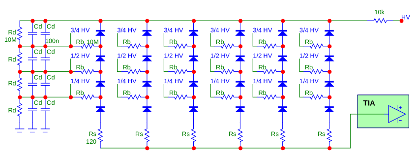
Figure 1 depicts the 4s6p topology where six branches each with four SiPMs are fed to a single TIA. In [5] we used four quadrants each with an individual TIA to read 24 SiPMs: each quadrant was configured with a 2s3p layout (three parallel branches of two SiPMs in series) and an active summing node was required to aggregate the signal from the four TIAs.
The 4s6p configuration drastically simplifies the scenario: only one pre-amplifier is required without other circuit elements. However, the stronger ganging reduces the signal by a factor two with respect to the 2s3p scenario. This happens because the capacitive coupling of the SiPMs in series attenuates the photo-current by the series order (4 in this case). The next section will demonstrate the possibility to maintain nearly the same signal to noise ratio as that of the 42s3p configuration. This is achieved by reducing the input noise of the TIA with a proper selection of the circuit elements.
3.2 Divider
A precision voltage divider is required to provide an even voltage bias distribution to all the devices. At cryogenic temperature, the DCR-induced current is in sub-picoampere, a region that is sensitive to surface leakages of the SiPMs or from the PCB. The passive divider, shown in Figure 1, is provided by four resistors. The accuracy of the bias distribution affects the quality of the signal. Assuming the operation at in liquid nitrogen, a disuniformity of in the resistor leads to an over-voltage spread of . This is reflected in the form of an equivalent variation of the gain between different SiPMs in the same tile. The value of defines the stability of the divider for current leakages of the SiPMs or of the PCBs: with = a SiPM surface leakage of (over ) would affect the divider by less than .
For the choice of , Vishay resistors MCT06030C1005FP500 have been selected as they provide a tolerance with very low temperature drift. Eight PEN capacitors (Panasonic ECW-U1104V33) are placed in parallel to the divider. The capacitors and the resistor form a filter for the noise coming from the bias line. The branch resistors decouple the SiPMs from each other and from the divider capacitors, thus eliminating unwanted paths to the signal. For convenience, same Vishay part for the branch resistors and for the divider resistors were used.
3.3 TIA
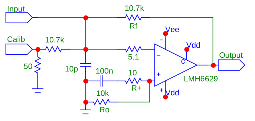
We used the trans-impedance amplifier (TIA) described in [7] that is based on the LMH6629 from Texas Instruments operating from . The chip exhibits a voltage input noise equivalent to a = resistor and an input current noise () that is below for temperatures lower than . The TIA is configured with a gain of with disabled compensation and without any feedback capacitor, see Figure 2(a).
For a generic tile configured with Q quadrants each with P parallel branches each of S SiPMs in series, the total input noise of the TIA in liquid nitrogen at can be calculated with the following formula:
| (3.1) |
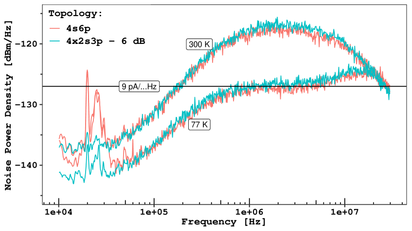
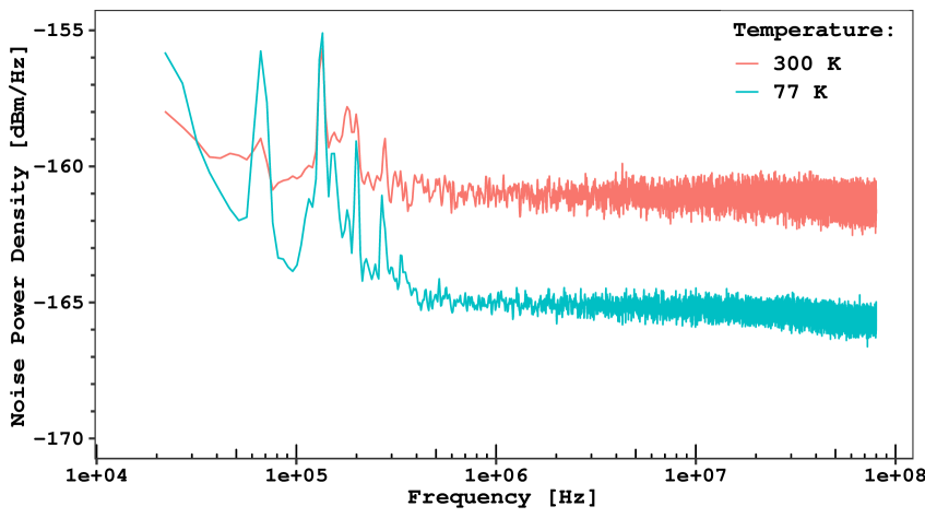
where the adder noise (if needed) is neglected and is the branch series resistor shown in Figure 1. At the pole at affects the noise gain by less than and therefore the formula for the noise simplifies to a non-inverting amplifier as in Equation 3.1. At lower frequencies, the noise gain is reduced by the presence of the pole and only the is relevant. At higher frequencies the parasitic capacitance of the quenching resistor () comes into play leading to an increased noise gain until the cut-off from amplifier bandwidth. Figure 2(b) reports the output noise spectra measured on the same tile configured in 4x2s3p and 4s6p. At room temperature , is smaller by a factor and the gain bandwidth product of the LMH6629 is one fourth [7]. Therefore, the cut-off happens within the noise gain plateau and spectra does not show any features.
3.4 Pulse Shape and SNR
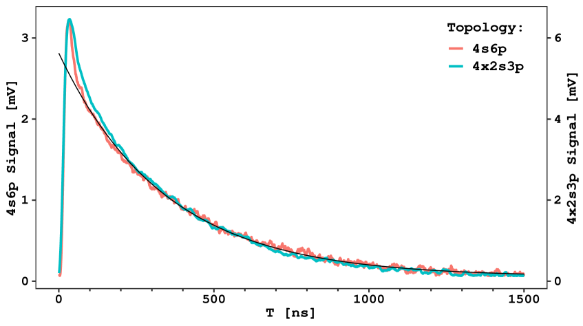
As described in [11], the recharge part of the signal of SiPMs includes two exponential components ( and ). The authors focused on small SiPMs, for which . This leads to the assumption . For large devices, such assumption breaks and it is necessary to solve the equations with ganged SiPMs. The value of = at leads to the degeneration of the two exponential components, resulting in a pure exponential recharge after the first , Figure 3(a).
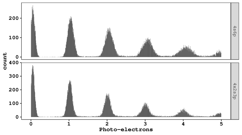
Concurrently with =, the input noise of the 4s6p tile is halved with respect to the noise of the 4x2s3p and =, as shown in Figure 2(b). Similarly, the signal amplitude for the 4s6p is halved, as shown in Figure 3(a). Since the signal shape and the noise bandwidth remain unaltered (as result of the identical noise gain), the signal to noise ratio (SNR) is preserved. The SNR is calculated as the gain of the system divided by its average baseline noise (in the pre-trigger window). Figure 3(b) reports the pulse spectrum for the same tile acquired in both configurations.
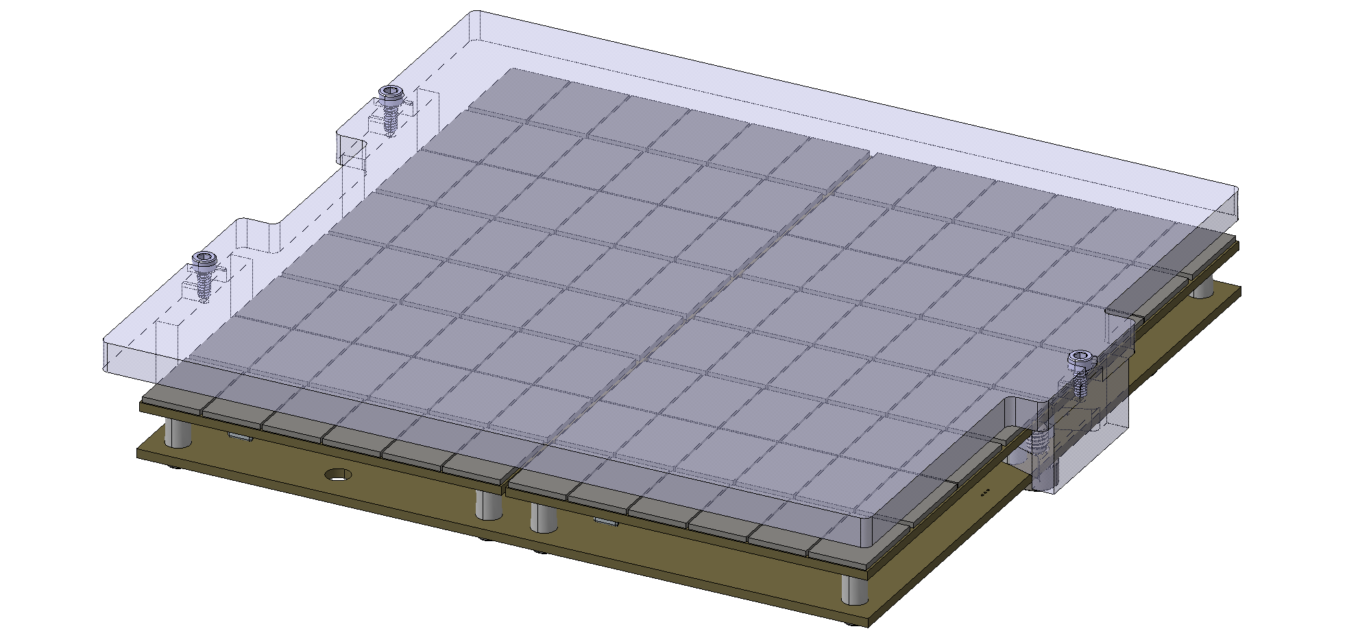
4 Tile+
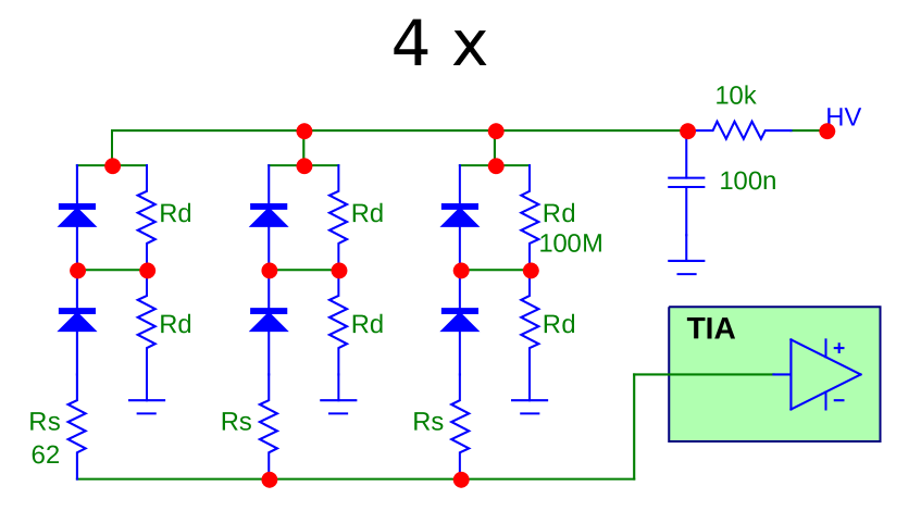
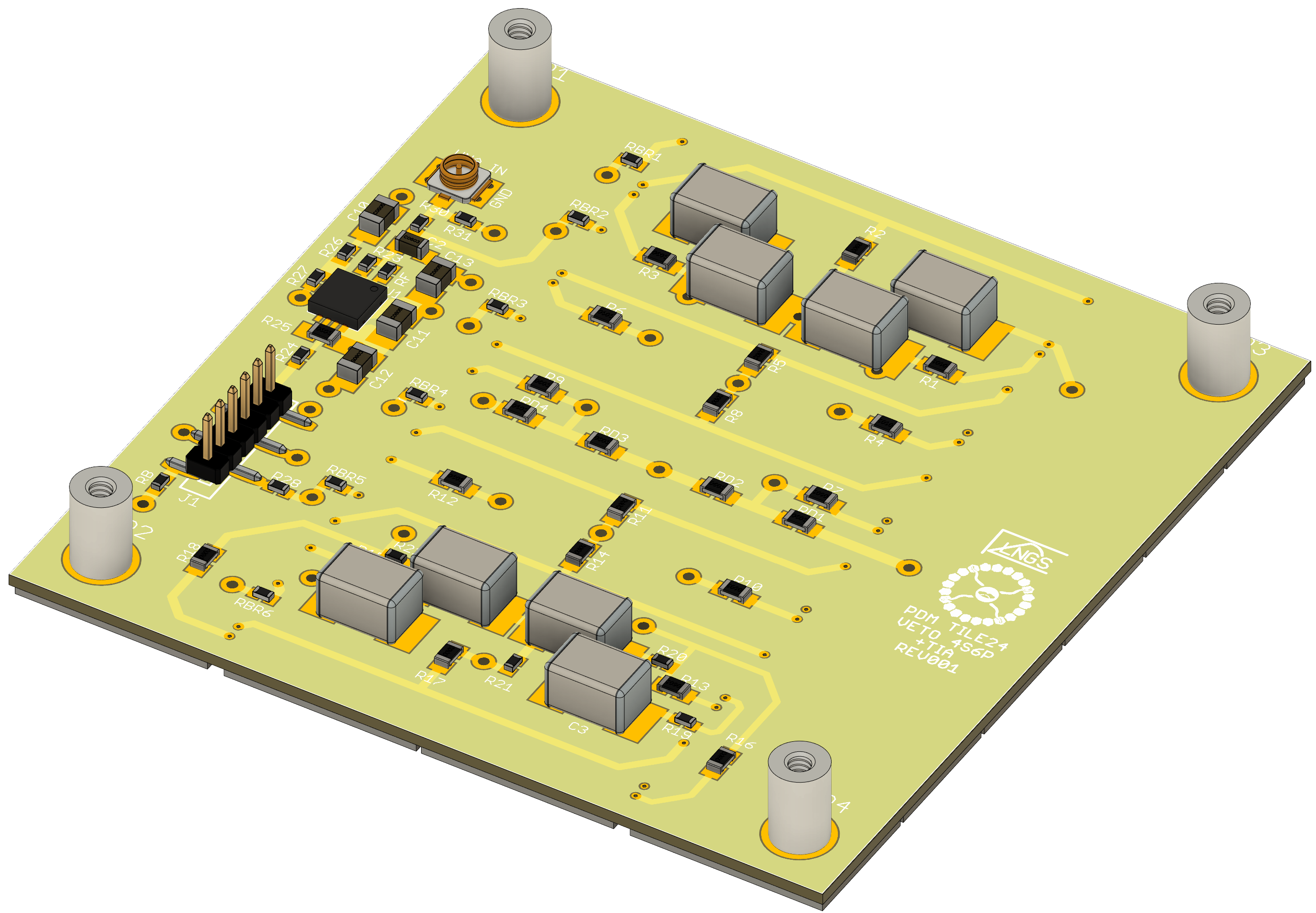
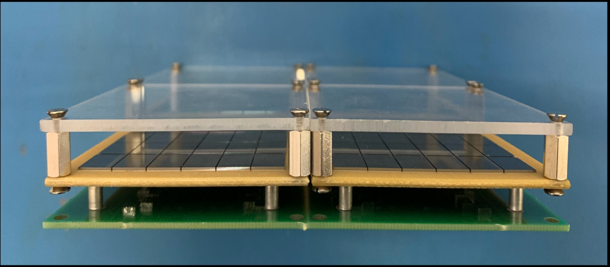
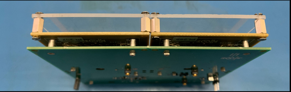
A Tile+ is a single unit including 24 SiPMs (top layer) and the required readout electronics (bottom layer). The 4s6p ganging scheme described earlier is used, therefore only one TIA is needed. Figure 4 depict the Tile+. The signal output, the HV bias, the ground and the low voltages () are routed on pin strip connector (M50-3630642 from Harwin).
Four threaded spacers (97730506330R from Wurth) are soldered to the PCB during the automatic population of bottom components in the first stage of the assembly. A low temperature Tin-Bismuth alloy is used to avoid damaging the PEN capacitors which, after reflow at high temperatures, tend to produce leakage in cryogenic environment.
After the validation of the electrical circuit in liquid nitrogen, the SiPMs are placed on the PCB using a Westbond 7200CR manual die bonder. We use an Indium-Tin solder (Indium Corp Indalloy#1E), dispensed automatically in six dots by an Auger valve installed on a fluid dispenser robot [12]. As final step, the tile is processed again in the reflow oven with a thermal profile compatible with the bottom components. The PCB finish and the SiPM backside are in gold. This provides good adhesion and avoids the formation of weak inter-metallic compounds with indium.
The dimension of the PCB is with a fill factor of . The PCB is realized in Arlon 55NT that exhibits low thermal shrinkage . This is necessary to avoid stress on the silicon that has a shrinkage of about [13].
In liquid nitrogen the Tile+ dissipates a power of with an output swing of (before back-termination), corresponding to about photo-electrons at . The performances in terms of SNR, signal shape and pulse spectrum remain unaltered with respect to what is shown in the previous section.
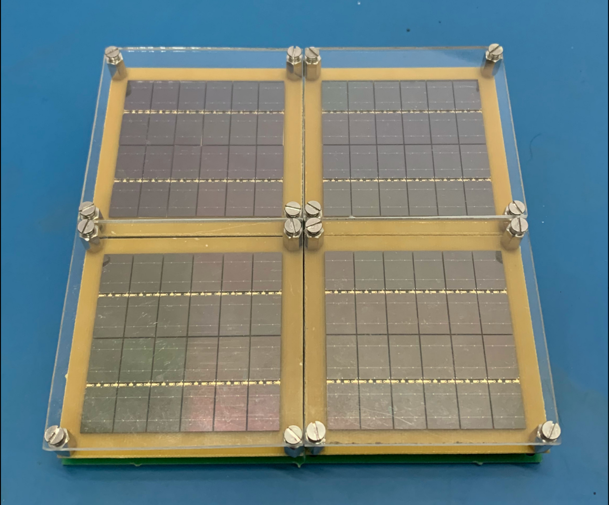
5 MB¼
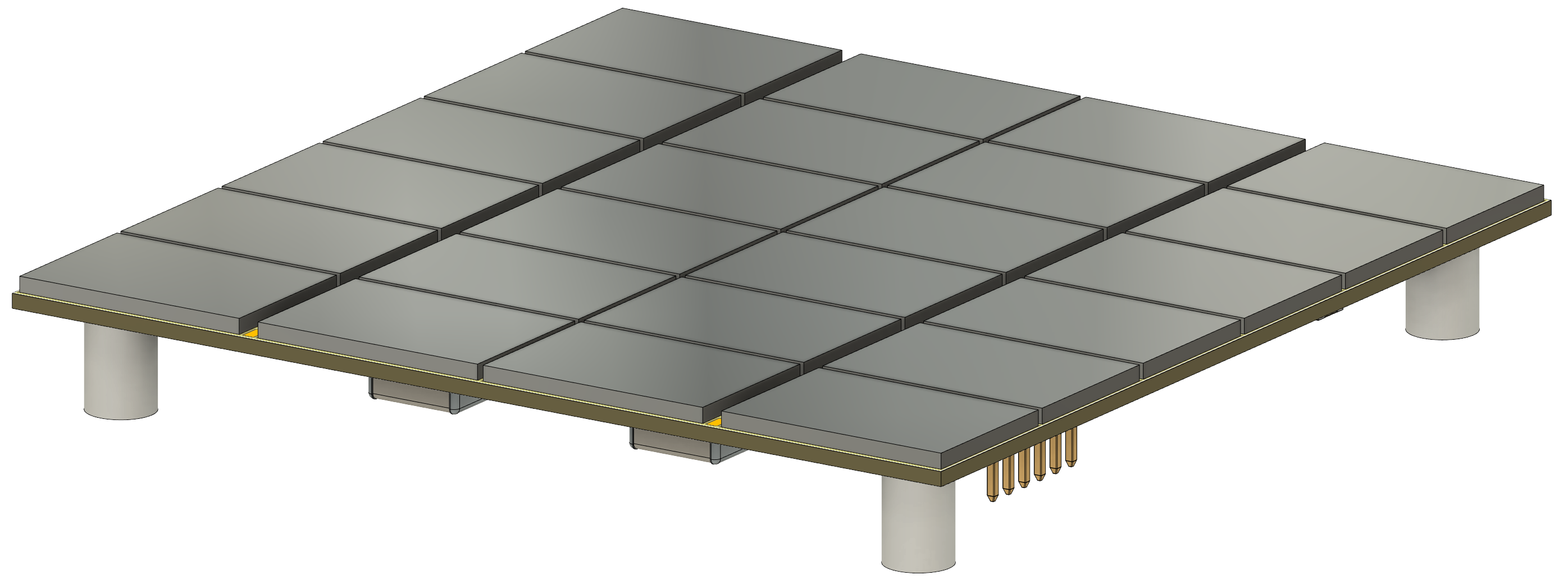
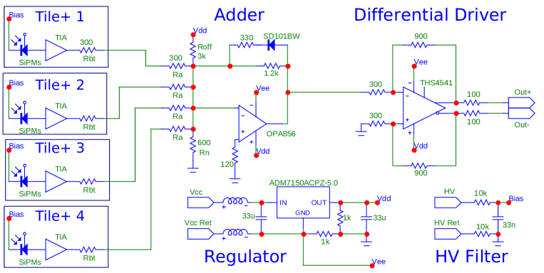
Given the very high SNR for the Tile+, it is possible to aggregate four tiles in a single analog photo-detector with a total surface of . The schematics of such device, called MB¼, is shown in Figure 5. The finished unit is shown in Figure 7 and in Figure 9.
5.1 Adder
The aggregation of the four Tile+ is performed by an analog adder with double gain. This circuit is based on a OPA856 from Texas Instruments, capable of working in liquid nitrogen with a gain bandwidth product of about , with a dissipation of on a power rail of . At cryogenic temperature the peak to peak output swing is limited to : to maximise the dynamic range for unipolar (positive) pulses, the output is biased at by the resistor, leaving a useful swing of . The small signals gain is , as defined by . The optional Schottky diode (SD101BW) provides a second gain of for large pulses. In liquid nitrogen and assuming an over-voltage of , without the diode the dynamic range is about 300 photo-electrons, that becomes 500 for the configuration with double gain, see Figure 6(a). The bandwidth of the adder at exceeds and therefore does not affect the pulse shape (the TIA is limited to ). Figure 6(b) reports the input noise equivalent for the adder: the comparison term is the output noise of the TIA, Figure 2(b), incremented by .
5.2 Differential Driver
A high dynamic range cryogenic fully differential transmitter has been developed to facilitate scaling up to many photo-detectors in a ground isolated environment (see later). The differential transmitter is based on a THS4541 from Texas Instruments. In liquid nitrogen, the chip is capable of driving low impedances ( transmission lines) with a large output swing (about differential) with a supply of and a power consumption of . To match the output swing of the adder (), a gain of per branch is used. Considering the loss of the single-ended to differential conversion (a factor ½), the amplitude of the single photo-electron becomes before the backside termination ( on the cable), which is well above the typical noise of a differential line for the bandwidth. Since the rise-time () of the transmitter with of cable is below and its input noise density is in the order of , the effects on the signal quality are negligible.
5.3 Voltage regulator
In the Tile+ and in the MB¼, the op-amps are configured as inverting amplifiers. Therefore, all the currents (input and output) sum to zero. As a consequence, it is feasible to create a local ground with a simple voltage divider (and proper bypass capacitors). The main advantage of this design due to the differential transmission, is that it keeps the local ground isolated from the receiver electronics and from the cryostat, which reduces ground loops and noise injection. To further reduce noise and ripple from the power supply, a low drop voltage regulator (LDO) to the system is added. The ADM7150ACPZ-5.0 from Analog Devices provides a protection from the accidental fluctuations of the power supply up to , works in liquid nitrogen with noise density in the range of and a drop of the order of . Therefore, the minimum power consumption of the fully instrumented MB¼ is x .
5.4 Connections
The MB¼ can be connected with standard unshielded RJ45/U. Categories above 5e satify the bandwidth and the FEP jacket is compatible with cryogenic environment. At room temperature, two isolated power supplies are required. A Keysight 3649A for the low voltage, and a Keithley 2450 SMU for the HV bias have been used for this purpose. The HV is internally filtered in the MB¼ with a circuit, that protects the local ground from noise injection.
The signal is delivered to a simple differential receiver implemented with a LMH6552 from Texas Instruments that matches the high dynamic range and low noise requirements. To limit the power dissipation due to the of baseline on the termination, an AC coupling on the receiver is required. Standard ceramic capacitors with the termination resistor provide a pole well outside the region of interest.
5.5 Performances
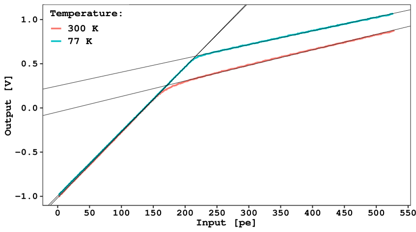
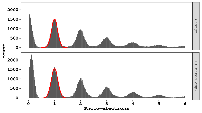
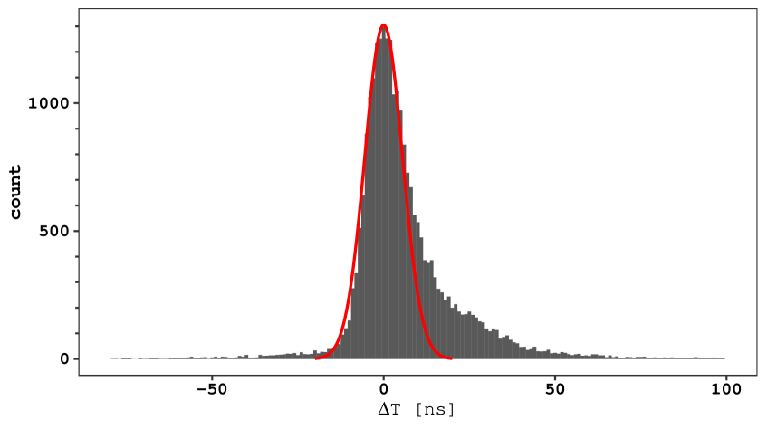
Figure 8(a) reports the pulse spectrum of the charge (in a 3 window) and of the filtered amplitude. The latter is based on matched filtering, that is the cross-correlation of raw waveform for the average signal, Figure 3(a). The result is a cusp-like signal (similar to ) whose maximum amplitude is used to populate the histogram of Figure 8(a). The location of the maximum provides accurate timing information as shown in Figure 8(b). The SNR for both charge and filtered signal is above and the resolution of the first photo-electron is around , dominated by the spread of the breakdown voltage, the disuniformities of the recharge time and the tolerance of the divider.
6 Conclusions
In this work, the design and the implementation of a very large SiPM array for cryogenic application has been documented. An SNR larger than with a resolution of the first photo-electron was demonstrated. This is for a photo-detector that includes x SiPMs. The timing resolution of this array is , a value better than several PMTs of the same size. The dynamic range exceeds photo-electrons with a power dissipation of . The operation of this unit requires standard laboratory power supplies and simple differential receiver.
Acknowledgements
We acknowledge support from the Istituto Nazionale di Fisica Nucleare (Italy) and Laboratori Nazionali del Gran Sasso (Italy) of INFN, from NSF (US, Grant PHY-1314507 for Princeton University), from the Royal Society UK and the Science and Technology Facilities Council (STFC), part of the United Kingdom Research.
References
- [1] DUNE collaboration, Prospects for beyond the Standard Model physics searches at the Deep Underground Neutrino Experiment, Eur. Phys. J. C 81 (2021) 322.
- [2] C.E. Aalseth et al., Darkside-20k: A 20 tonne two-phase lar tpc for direct dark matter detection at lngs, Eur. Phys. J. Plus 133 (2018) .
- [3] E. Aprile et al., Projected WIMP sensitivity of the XENONnT dark matter experiment, JCAP 11 (2020) 031.
- [4] DARWIN collaboration, DARWIN: towards the ultimate dark matter detector, JCAP 11 (2016) 017.
- [5] M. D’Incecco, C. Galbiati, G.K. Giovanetti, G. Korga, X. Li, A. Mandarano et al., Development of a novel single-channel, 24 cm2, sipm-based, cryogenic photodetector, IEEE Trans. Nucl. Sci. 65 (2018) 591.
- [6] F. Acerbi, S. Davini, A. Ferri, C. Galbiati, G.K. Giovanetti, A. Gola et al., Cryogenic Characterization of FBK HD Near-UV Sensitive SiPMs, IEEE Trans. Elec. Dev. 64 (2017) 521.
- [7] M. D’Incecco, C. Galbiati, G.K. Giovanetti, G. Korga, X. Li, A. Mandarano et al., Development of a Very Low-Noise Cryogenic Preamplifier for Large-Area SiPM Devices, IEEE Trans. Nucl. Sci. 65 (2018) 1005.
- [8] A. Gola, F. Acerbi, M. Capasso, M. Marcante, A. Mazzi, G. Paternoster et al., Nuv-sensitive silicon photomultiplier technologies developed at fondazione bruno kessler, Sensors 19 (2019) .
- [9] Boulay, M. G., Camillo, V., Canci, N., Choudhary, S., Consiglio, L., Flammini, A. et al., Direct comparison of pen and tpb wavelength shifters in a liquid argon detector, Eur. Phys. J. C 81 (2021) 1099.
- [10] M.G. Boulay, V. Camillo, N. Canci, S. Choudhary, L. Consiglio, A. Flammini et al., Sipm cross-talk in liquid argon detectors, 2021, [2201.01632].
- [11] D. Marano, M. Belluso, G. Bonanno, S. Billotta, A. Grillo, S. Garozzo et al., Silicon photomultipliers electrical model extensive analytical analysis, IEEE Transactions on Nuclear Science 61 (2014) 23.
- [12] I. Kochanek, Packaging strategies for large sipm-based cryogenic photo-detectors, Nucl. Instrum. Methods Phys. Res. A 980 (2020) 164487.
- [13] I. Kochanek, SiPMs for cryogenic temperature, Nuovo Cim. C 42 (2019) 62.