Relaxing graphene plasmon excitation constraints through the use of an epsilon-near-zero substrate
Abstract
Graphene plasmons have attracted significant attention due to their tunability, potentially long propagation lengths and ultracompact wavelengths. However, the latter characteristic imposes challenges to light-plasmon coupling in practical applications, generally requiring sophisticated coupling setups, extremely high doping levels and/or graphene nanostructuting close to the resolution limit of current lithography techniques. Here, we propose and theoretically demonstrate a method for alleviating such a technological strain through the use of a practical substrate whose low and negative dielectric function naturally enlarges the graphene polariton wavelength to more manageable levels. We consider silicon carbide (SiC), as it exhibits a dielectric function whose real part is between -1 and 0, while its imaginary part remains lower than 0.05, in the 951 to 970 cm-1 mid-infrared spectral range. Our calculations show hybridization with the substrate’s phonon polariton, resulting in a polariton wavelenth that is an order of magnitude longer than obtained with a silicon dioxide substrate, while the propagation length increases by the same amount.
pacs:
Valid PACS appear hereI Introduction
Plasmons, the collective oscillation of free electrons in a conductive material, have attracted great attention in the field of nanophotonics due to its high confinement of electromagnetic energy, achieving subdifractional spatial extensionsabajoch ; maier , which allows for the construction of photonic devices at the nanometer scale. The applications range from biosensingbio1 ; bio2 ; bio3 to enhanced spectroscopy techniques such as SERSsers1 ; sers2 ; sers3 , TERSters1 ; ters2 ; ters3 ; ters4 and SNOMsnom1 ; snom2 ; snom3 ; snom5 ; snom5 ; snom6 .
Graphene, a two-dimensional material consisting of a single layer of carbon atoms in a hexagonal latticegeim-nov-2004 , has emerged as a promising material for plasmonic applications due to its high electronic mobility and null bandgap, which allows for high Fermi level tunability and significant changes on the optical conductivitykoppens ; pol-2d . Since the plasmon dispersion is dependent on the electronic density, graphene plasmons can be actively controlled more easily than those in conventional conductorsfang . Also, graphene can be transfered to a range of dielectric surfaces, allowing for the integration of graphene-based plasmonic devices with photonic devices, such as silicon-based waveguideslivro-nuno .
The plasmon wavevector in graphene tends to be up to 2 orders of magnitude larger than that of free space radiation in the mid-infrared range. However, efficient radiation-plasmon coupling, for the excitation of surface plasmon polaritons (SPPs), requires circumventing the large wavevector mismatch. For bridging such a high mismatch, finding a suitable high-index dielectric material for prism couplingotto ; kre becomes impractical, while diffraction grating coupling has required structures with periodicity of tens of nanometersgrating1 ; grating2 ; grating3 , posing a strain on the device fabrication step. Alternatively, localized surface plasmons (LSPs) have been excited in graphene patterned into nanostructures such as nanoribbons or nanodisksju ; Rodrigo ; fang2 . Again, due to the large wavevector mismatch, the features in these structures need to be in the tens to hundreds of nanometers range, for operation in the mid-infraredRodrigo ; fang ; vasic . Even though such structures have been fabricated and used to excite graphene plasmons, the fabrication of such devices is challenging due to their size being close to the spatial resolution limit of current nanofabrication techniquesnikitin .
The plasmon dispersion in graphene is dependent on the dielectric function of the adjacent media. Therefore, the choice of the substrate plays a key role in the wavevector matching for plasmon excitation. In particular a decrease in the magnitude of the plasmon wavevector is expected for a substrate with a low permittivityabajoch ; livro-nuno . The plasmon wavevector is proportional to the sum of the dielectric functions of the substrate and superstrate. If we consider the latter to be air, meaning a dielectric function equal to 1, the optimal choice of substrate would be one with dielectric function of -1. However, a common drawback of materials with a negative dielectric function is that the imaginary part of the dielectric function cannot be neglected, leading to plasmon losses.
Epsilon-near-zero (ENZ) materials have received considerable recent attention for a number of interesting properties, including increased nonlinear optical susceptibilitiesAlam , which can be used to enhance nonlinear effects such as second harmonic generationpilar , and wavelength enlargement, which allows light tunneling through narrow channelssilveirinha . As in plasmonics, ENZ applications also require a low imaginary dielectric function component at the spectral range where the real dielectric function is low. As a consequence, ENZ materials are also good candidates for plasmonic applications. Indeed, they have been studied in the field of plasmonics for being capable of directly coupling SPPs to free-space lighttraviss .
Silicon carbide is an ENZ material in the mid-infrared due to its optical phononstiwald ; engheta1 ; engheta2 . The range between the transverse optical phonon (TO), at 797 cm-1, and the longitudinal optical phonon (LO), at 970 cm-1, called the Reststrahlen band, exhibits a real negative dielectric function, with the function crossing zero at both these wavenumbers.caldwell ; koch . In particular, a low imaginary part of epsilon is obtained near the LO phonon wavenumber. Within the Reststrahlen band, the material also supports surface phonon polaritons (SPhP)koch ; huber ; sic1 ; sic2 . It has been shown that when graphene plasmons are excited within the Reststrahlen band of a SiC substrate, hybrid plasmon-phonon modes arise, which maintain the characteristics of both excitations, exhibiting a longer wavelength than a pure SPP and keeping losses lowhy1 ; hy2 ; hy3 ; sic3 ; sic4 . The use of SiC is also convenient since graphene can be epitaxially grown directly onto this substrateepi1 ; epi2 ; epi3 ; epi4 ; epi5 . Other polar dielectrics have also been studied as substrates for graphene plasmonics due to their ENZ naturehy1 ; hy2 ; hy3 , however, ENZ substrates have not been used for increasing the graphene plasmon wavelength with the purpose of reducing the wavevector mismatch for optical excitation. In this work, we propose the use of SiC as a graphene substrate for mitigating this mismatch in the mid-infrared. Our results show an increase from hundreds of nanometers to a few micrometers in polariton wavelength on SiC when compared with a SiO2 substrate. This simplifies the polaritonic excitation while keeping the polariton modal volume 3 orders of magnitude smaller than that of free-space radiation. Although there is a loss of confinement, these polaritonic waves become easier to excite, and the fabrication of polariton-based devices becomes easier. The conditions for this trade-off can be adjusted by tailoring the size of the structures used for excitation and controlling the graphene doping.
II Methods
To obtain the graphene plasmon dispersion, we used the condition for SPP formationabajoch :
| (1) |
where is the plasmon wavenumber, is the free-space radiation wavenumber, is the graphene optical conductivity, , are the dielectric functions of the superstrate, substrate, respectively, and is the vacuum permittivity.
We assume graphene to be on the interface between air ( = 1) and either SiC or SiO2. We use the Drude model for the graphene conductivityabajoch ; livro-nuno :
| (2) |
where is the electron charge, is the Fermi energy and is the relaxation rate. This is a good approximation when the temperature is low and electronic density is high. Also, non-local effects are neglected. These are considered important only for small nanostructures and when graphene is near metallic surfacesnature-nuno . The value of the relaxation time is assumed to be such that meVfei1 . The dielectric function for SiO2 was taken to be given bykarimi .
| (3) |
with = 2.3 and using the parameters shown in Table 1. The dielectric function of SiC was taken to be given bydong
| (4) |
with , = 120.5 meV, = 98403 meV and = 5.9 meV.
| (meV) | (meV2) | (meV) |
|---|---|---|
| 142 | 812 | 7.4 |
| 133 | 7832 | 5.4 |
| 100 | 537 | 4 |
| 57 | 3226 | 6.2 |
| 47 | 1069 | 24.5 |
We numerically solved equation 1 for obtaining the in-plane wavevector , from which we can calculate both the polariton wavelength () and the effective propagation length (). To better understand the plasmon-phonon interaction, we also calculated the loss function, given by the imaginary part of the p-polarized reflectivity rplivro-nuno :
| (5) |
where and are the wavevectors of light propagating in air and the substrate, respectively.
We have also calculated the reflectance and absorbance spectra for an array of graphene ribbons in order to determine the corresponding LSP resonance condition. Since the conductivity of a regular array of graphene nanoribbons is spatially periodic (, where is the periodicity), the reflected and transmitted fields can be expressed by a Fourier-Floquet series. Matching the boundary conditions at the interface, we arrive at the linear system of equations: livro-nuno
| (6) |
where , , and . The Kronecker delta signals that the incident field only appears for the diffraction order . The Fourier coefficients of the conductivity are calculated assuming that the width of the graphene nanoribbon in the unit cell is , and has the same conductivity of a graphene sheet (). Once, the fields are obtained the reflectance, transmittance and absorbance are respectively calculated as:
| (7) | |||
| (8) | |||
| (9) |
III Results and discussion
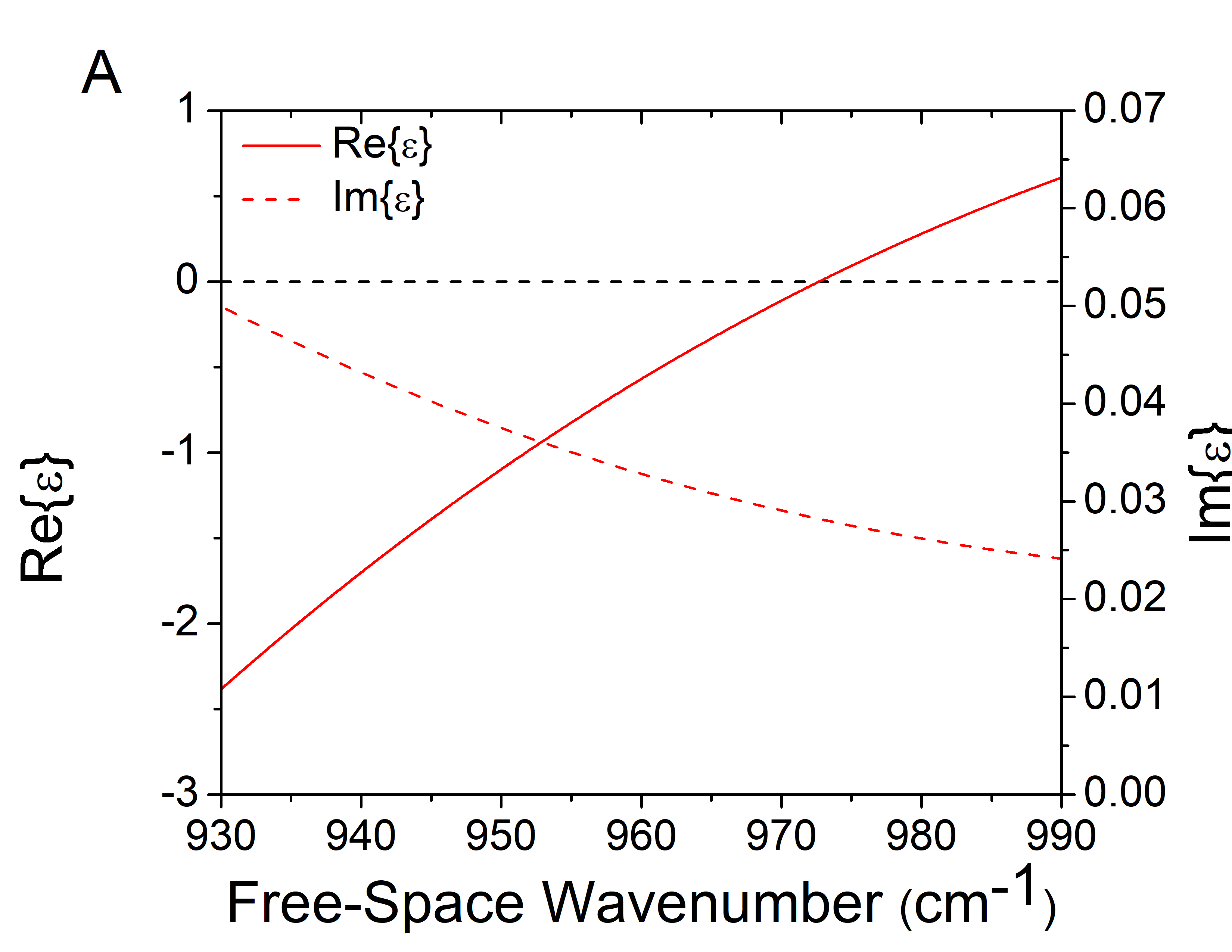
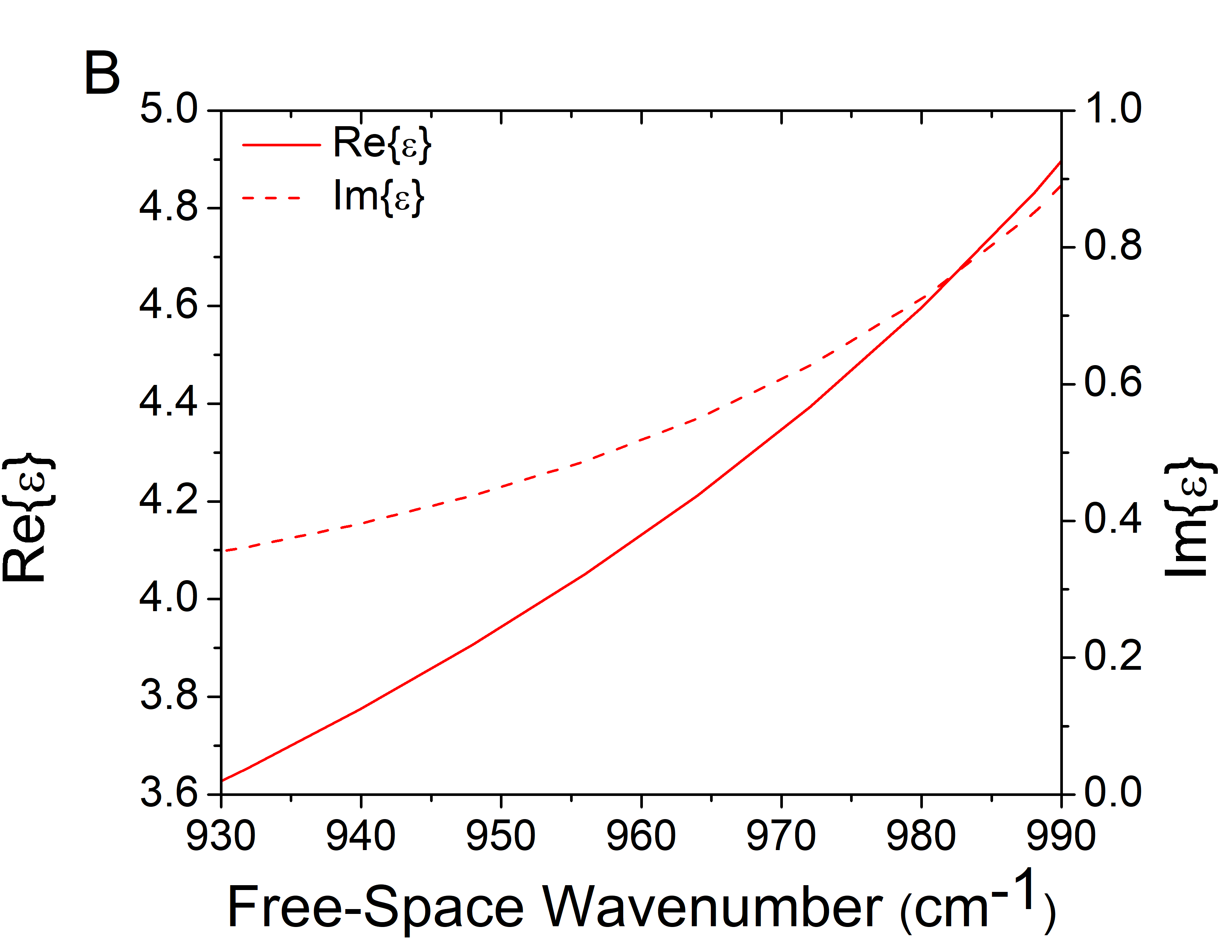
Figures 1A and B show the dielectric functions of SiC and SiO2, respectively. For silicon carbide the real part of the dielectric function is equal to zero at 970 cm-1. At 951 cm-1 the real dielectric function is -1 and the corresponding imaginary part is , meaning that polaritonic losses are expected to be low. In the same spectral region, SiO2 has a real dielectric function of 4 to 5, with a much higher immaginary part of around 0.4 to 0.8, meaning that the graphene plasmon wavelength is expected to be shorter and propagation losses are expected to be higher.
Figures 2A and B respectively show the polariton wavelength and effective propagation length as functions of free-space wavenumber calculated by solving eq. 1 for an air/SiC interface with and without graphene with a Fermi energy of 0.4 eV. We focus this analysis in the spectral region where the real dielectric function of the substrate is between 0 and -1. Without graphene this system should not, in principle, exhibit surface phonon polaritons for an excitation wavenumber beyond 951 cm-1, as , not allowing for polaritons. However, because of the imaginary part of , a mode arises with very high losses between 951 and 970 cm-1, where the sum of the real dielectric functions is close to zero. The addition of graphene to the interface allows for the excitation of lower loss plasmon-phonon polaritons above 951 cm-1, which is expressed by a shorter wavelength and a longer propagation length. For lower wavenumbers, within the Reststrahlen band, graphene imposes only a minor change to the wavelength, which suggests that in that region the polariton would exhibit a dominant SPhP character.
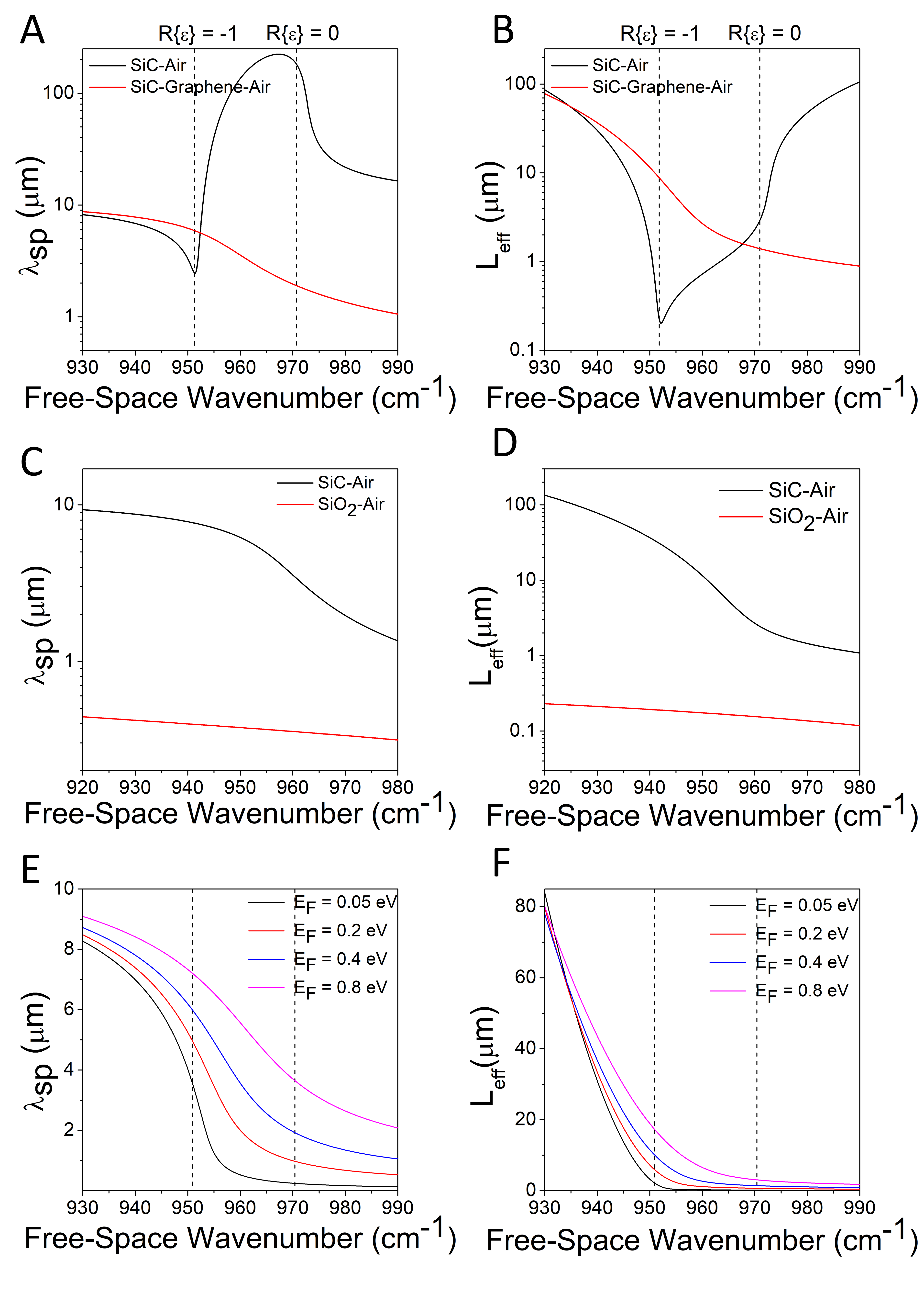
Figures 2C and D show a comparison of the polariton wavelength and propagation length using SiC and SiO2 as the substrate. At the spectral range where the real dielectric function of SiC lies between -1 and 0, an order of magnitude increase in polariton wavelength is obtained. At 951 cm-1, for example, the plasmon wavelength is 0.4 m on SiO2 and 5.8 m on SiC. As for propagation length, it is 0.2 m for SiO2 and 9 m for SiC. Note that for SiO2, the propagation length is shorter than the polariton wavelentgh, while for SiC, the propagation length is longer. The combination of longer wavelength and propagation lengths makes polaritonic devices based on graphene on SiC simultaneously easier to fabricate and more efficient. Note that despite the polariton wavelength increase, it remains about half the light wavelength at the same frequency, allowing for subdiffractional devices to be designed. The optimal wavelength for a polaritonic device can be tailored by changing the free-space wavenumber or adjusting graphene’s Fermi level.
Figures 2E and F respectively show the polariton wavelength and propagation length for various graphene Fermi energies, ranging from 0.05 eV to 0.8 eV. As expected, increases with EF. At 951 cm-1, for example, Fermi energies of 0.2, 0.4 and 0.8 eV result in plasmon wavelengths of approximately 4.9, 6 and 7.2 m, respectively. Once again we notice that the propagation length also increases. For the same Fermi energies, we get propagation lengths of 5.8, 10 and 17.3 m. Even for a low graphene doping such as 0.2 eV we get a much longer polariton wavelength and propagation length, on the order of micrometers, than with a SiO2 substrate, which results in wavelengths of hundreds of nanometers, with much higher losses.
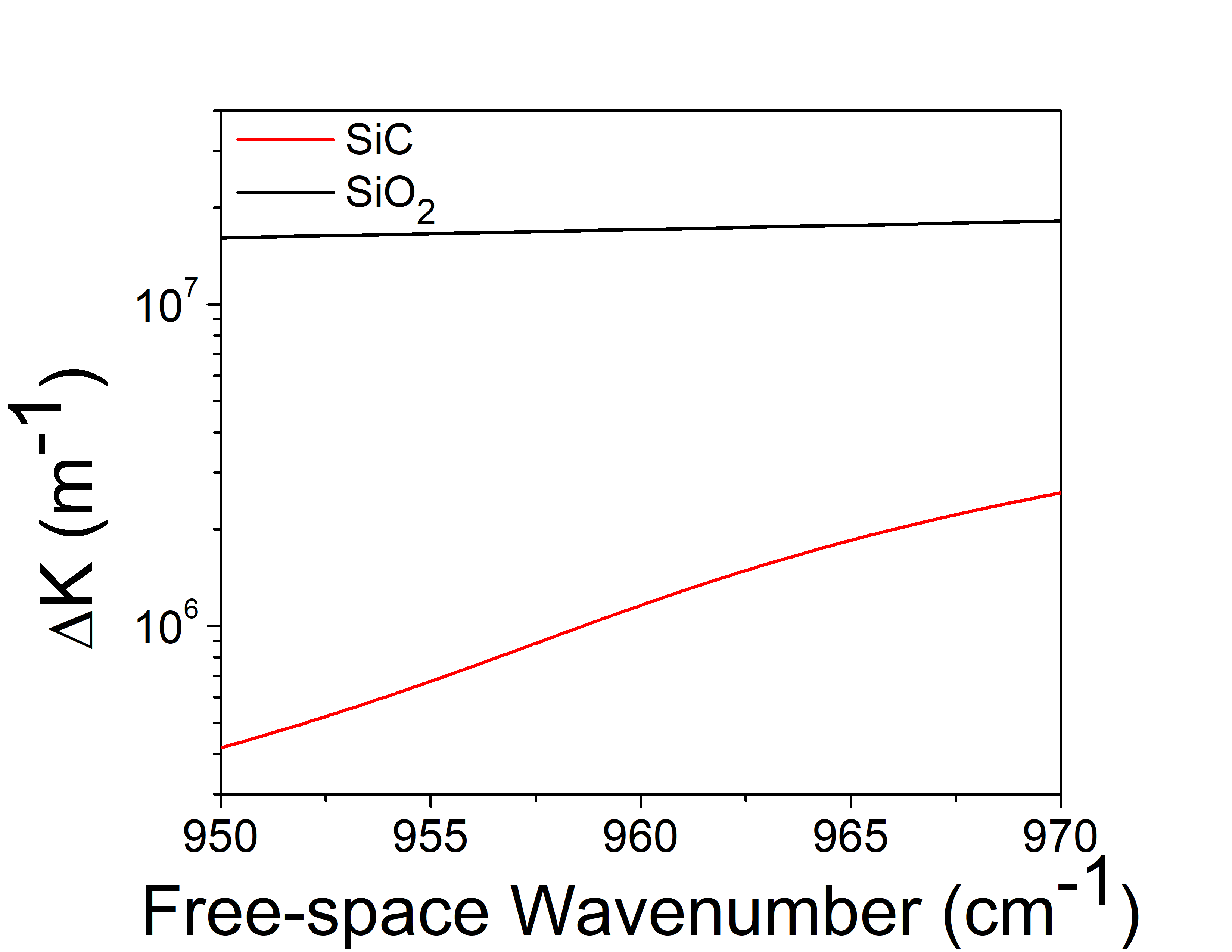
In order to easily visualize the wavevector mismatch between free-space radiation and the polariton wave in graphene on the two different substrates, we plot, in Figure 3, , where is the free-space light wavelength, for both SiC and SiO2 as substrates. We consider a graphene with 0.4 eV Fermi energy. A decrease of more than an order of magnitude in K is obtained by using SiC. The lower wavevector mismatch between polariton and free-space radiation makes the fabrication of polaritonic devices simple. Even if we consider a graphene with a low doping of 0.2 eV, as our results show, the polariton wavelength is 4.9 m, meaning an excitation grating, for example, with a periodicity of 2.45 m (considering it to be half the wavelength). Such a feature size is easily fabricated with simple photolitography, rather than electron beam lithography, commonly used for conventional graphene plasmonic devices.
.
Since patterned graphene is one of the most convenient ways to build plasmonic devices, we now analyze the case of localized surface plasmons in microstructured graphene. We consider ribbon widths, , from 0.5 to 2 µm, and fix the ribbon array periodicity at . Figures 4A and B show the reflectance and absorbance spectra for various ribbon widths with a 0.4 eV Fermi energy. Since silicon carbide has a negative dielectric function below 970 cm-1, for lower wavenumbers the material has a high reflectance, which is seen as a step in reflectance spectra. The polaritonic resonance is observed as a localized dip in reflectance and as peaks in absorbance. The resonance point can be tuned by adjusting the ribbon width and for excitation at 951 cm-1 2 m ribbons are required. With and 0.5 m the polariton resonance is at 951 and 964 cm-1, respectively. Figures 4C and D show the same calculations for different Fermi energies considering 1 m wide ribbons. Fermi energies of 0.2, 0.4 and 0.8 eV present polaritonic resonances at 952, 954 and 961 cm-1 respectively. Our calculations, therefore, show that the resonances in this spectral region can be excited using structures on the scale of micrometers, which alleviate the strain on fabrication. The absorbance peak that remains still () while the doping level and period of the graphene array are modified is produced by bulk evanescent waves in the substrate (SiC). It is important to notice that this peak is present even without the excitation of the surface polaritons.C8NR01706A
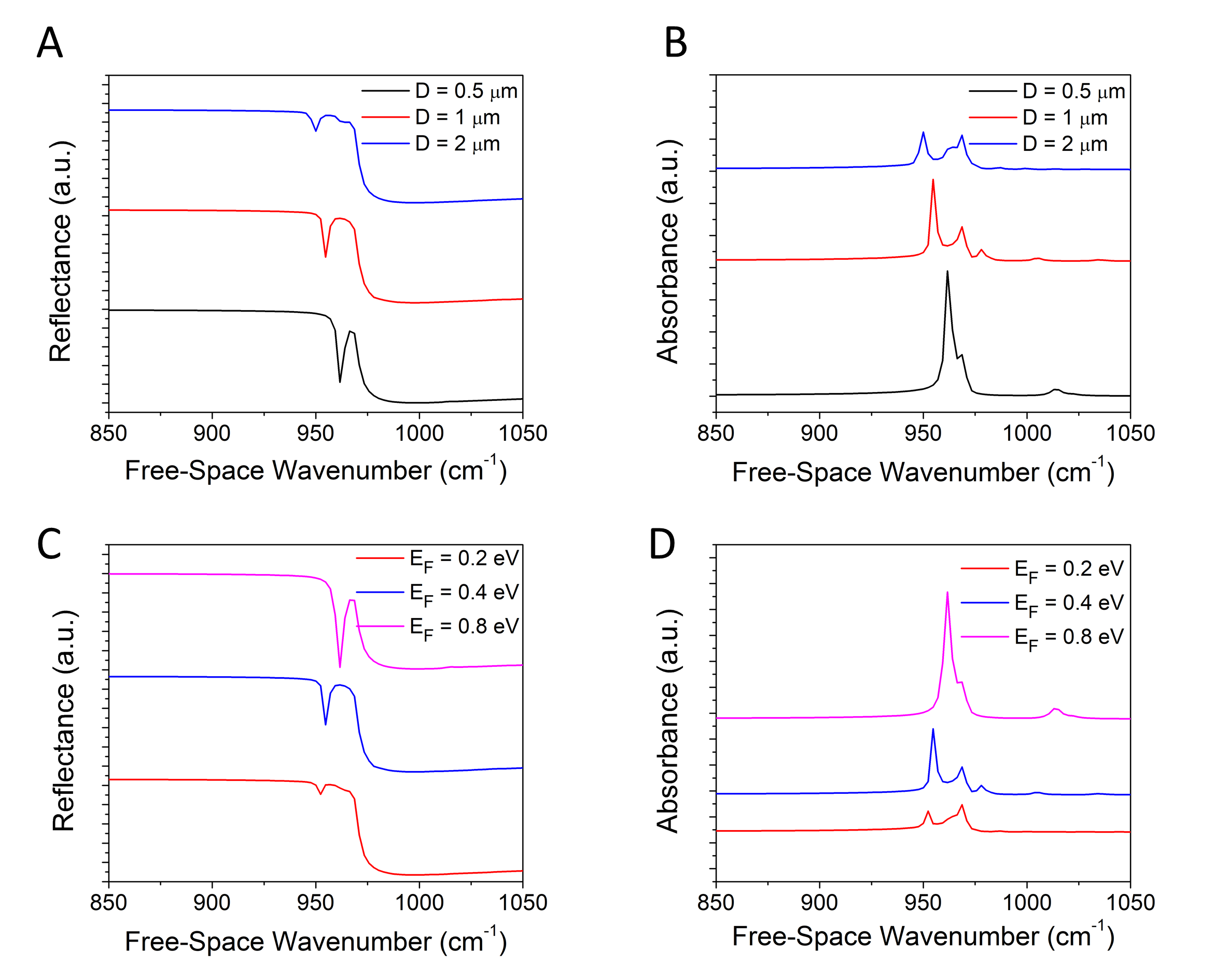
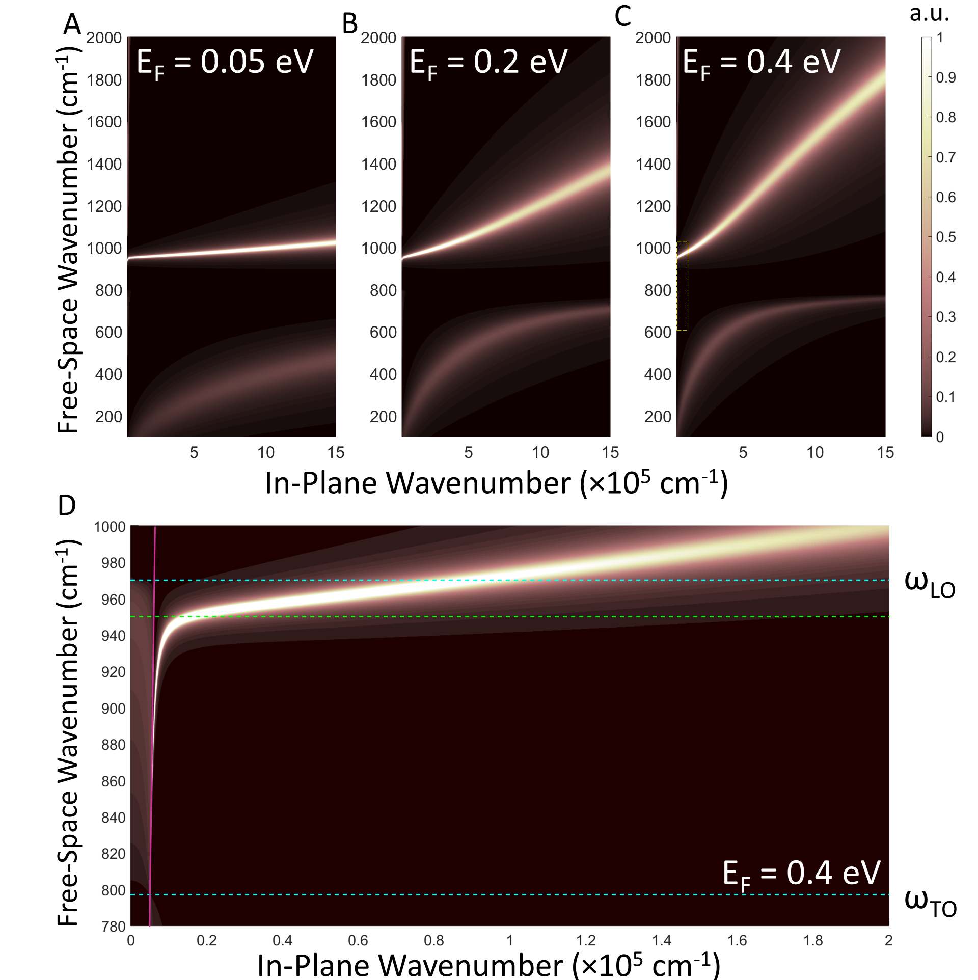
Figure 5 shows the calculated loss function for graphene at an air-SiC interface at various doping levels, through which the polariton dispersion relation can be visualized as bright yellow/white lines. Figures 5A-C show the polariton dispersion for graphene with a Fermi energy of 0.05, 0.2 and 0.4 eV, respectively. If there was no graphene at the interface, the only polariton solution would correspont to a straight horizontal line at the SiC’s SPhP frequency (represented by the dashed green line at 5D). When graphene is added to the interface, plasmon-phonon polariton hibridization takes place upon an anti-crossing of the dispersion relations, yielding 2 polariton branches, which shift towards higher free-space wavenumbers as the graphene Fermi level increases. As a general rule, the hybridized modes behave more like an SPP for low free-space wavenumbers and more like an SPhP for higher free-space wavenumberslivro-nuno . Figure 5D shows a zoom of Figure 5C at the area indicated by the yellow rectangle. The dashed cyan lines represent the wavenumbers of the LO and TO SiC phonons, the dashed green line represents the point where Re = -1, which is also the point where SPhP would appear for SiC without graphene and the magenta line represents light propagation through silicon carbide. The long polariton wavelengths reported here correspond to the upper hibrid polariton branch.
It should be noted that similar hybridization takes place near the optical phonon wavenumbers of other polar dielectrics used as substrates. In fact, the same effect can be observed in SiO2 at 1184 cm-1, where its dielectric function equals -1. However, we calculate that the polariton wavelength reaches a more moderate value of 1.2 m, with a corresponding sub-wavelength propagation length of 0.9 m. When compared with SiC, the shorter polariton wavelength and propagation lengths are a consequence of SiO2’s imaginary dielectric function, which remains high, 0.6 at the 1184 cm-1, at the epsilon near zero point. Therefore we can conclude that, although polariton wavelength increase can be achieved for other polar dielectrics, SiC is a more efficient substrate due to its lower losses.
IV Conclusions
We have demonstrated a method for increasing the wavelength of graphene polaritons in order to relax the conditions for matching their wavevector with that of free-space radiation. For this purpose, we choose a substrate with a real dielectric function between -1 and 0 in the mid-infrared region: silicon carbide. In the 951 to 970 cm-1 spectral range, we observe an order of magnitude polariton wavalength increase relative to SiO2 as a substrate, which is accompanied by an order of magnitude increase in propagation length. Due to the Reststrahlen band formed by phonons in the crystal, graphene plasmons hybridize with SiC phonons, allowing for the wavelength increase, which makes the excitation of polaritons with launching gratings easier. Along the same lines graphene structures of up to 2 m can be used for localized surface plasmon excitation. These result confirm SiC as a convenient substrate for graphene plasmonics, allowing for simple and large scale microfabrication methods to be employed, which can contribute to the more widespread use of graphene-based subdifractional photonics in real world applications.
V Acknowledgements
This work was funded by FAPESP (grant nos. 2015/11779-4, 2018/07276-5 and 2018/25339-4), the Brazilian Nanocarbon Institute of Science and Technology (INCT/Nanocarbon), CAPES-PRINT (grant no. 88887.310281/2018-00) and CAPES-PROSUC. NMRP acknowledges support by the Portuguese Foundation for Science and Technology (FCT) in the framework of the Strategic Funding UIDB/04650/2020, support from the European Commission through the project “Graphene-Driven Revolutions in ICT and Beyond” (Ref. No. 881603, CORE 3), COMPETE 2020, PORTUGAL 2020, FEDER and the FCT through project POCI-01-0145-FEDER-028114.
References
- [1] F. Javier García de Abajo. Graphene plasmonics: Challenges and opportunities. ACS Photonics, 1(3):135–152, 2014.
- [2] SA Maier. Plasmonics: Fundamentals And Applications, page 245. 01 2007.
- [3] Chengjun Huang, Jian Ye, Shuo Wang, Tim Stakenborg, and Liesbet Lagae. Gold nanoring as a sensitive plasmonic biosensor for on-chip dna detection. Applied Physics Letters, 100(17):173114, 2012.
- [4] Lin Wu, Hong-Son Chu, Wee Shing Koh, and Er-Ping Li. Highly sensitive graphene biosensors based on surface plasmon resonance. Optics express, 18:14395–400, 07 2010.
- [5] Shuwen Zeng, Kandammathe Valiyaveedu Sreekanth, Jingzhi Shang, Ting Yu, Chih-Kuang Chen, Feng Yin, Dominique Baillargeat, Philippe Coquet, Ho-Pui Ho, Andrei V. Kabashin, and Ken-Tye Yong. Graphene–gold metasurface architectures for ultrasensitive plasmonic biosensing. Advanced Materials, 27(40):6163–6169, 2015.
- [6] Kyle C. Bantz, Audrey F. Meyer, Nathan J. Wittenberg, Hyungsoon Im, Özge Kurtuluş, Si Hoon Lee, Nathan C. Lindquist, Sang-Hyun Oh, and Christy L. Haynes. Recent progress in sers biosensing. Phys. Chem. Chem. Phys., 13:11551–11567, 2011.
- [7] Shan Cong, Zhen Wang, Wenbin Gong, Zhigang Chen, Weibang Lu, John Lombardi, and Zhigang Zhao. Electrochromic semiconductors as colorimetric sers substrates with high reproducibility and renewability. Nature Communications, 10, 02 2019.
- [8] Hiang Kwee Lee, Yih Hong Lee, Charlynn Sher Lin Koh, Gia Chuong Phan-Quang, Xuemei Han, Chee Leng Lay, Howard Yi Fan Sim, Ya-Chuan Kao, Qi An, and Xing Yi Ling. Designing surface-enhanced raman scattering (sers) platforms beyond hotspot engineering: emerging opportunities in analyte manipulations and hybrid materials. Chem. Soc. Rev., 48:731–756, 2019.
- [9] Alyssa B. Zrimsek, Naihao Chiang, Michael Mattei, Stephanie Zaleski, Michael O. McAnally, Craig T. Chapman, Anne-Isabelle Henry, George C. Schatz, and Richard P. Van Duyne. Single-molecule chemistry with surface- and tip-enhanced raman spectroscopy. Chemical Reviews, 117(11):7583–7613, 2017. PMID: 28610424.
- [10] Prabhat Verma. Tip-enhanced raman spectroscopy: Technique and recent advances. Chemical Reviews, 117(9):6447–6466, 2017. PMID: 28459149.
- [11] Elena Bailo and Volker Deckert. Tip-enhanced raman scattering. Chem. Soc. Rev., 37:921–930, 2008.
- [12] Weitao Su, Naresh Kumar, Andrey Krayev, and Marc Chaigneau. In situ topographical chemical and electrical imaging of carboxyl graphene oxide at the nanoscale. Nature Communications, 9, 12 2018.
- [13] Peter Hermann, Bernd Kästner, Arne Hoehl, Vyacheslavs Kashcheyevs, Piotr Patoka, Georg Ulrich, Jörg Feikes, Markus Ries, Tobias Tydecks, Burkhard Beckhoff, Eckart Rühl, and Gerhard Ulm. Enhancing the sensitivity of nano-ftir spectroscopy. Opt. Express, 25(14):16574–16588, Jul 2017.
- [14] Sergiu Amarie, Paul Zaslansky, Yusuke Kajihara, Griesshaber Erika, Wolfgang Schmahl, and Fritz Keilmann. Nano-ftir chemical mapping of minerals in biological materials. Beilstein journal of nanotechnology, 3:312–23, 04 2012.
- [15] Alexandre Dazzi and Craig B. Prater. Afm-ir: Technology and applications in nanoscale infrared spectroscopy and chemical imaging. Chemical Reviews, 117(7):5146–5173, 2017. PMID: 27958707.
- [16] Hans A. Bechtel, Eric A. Muller, Robert L. Olmon, Michael C. Martin, and Markus B. Raschke. Ultrabroadband infrared nanospectroscopic imaging. Proceedings of the National Academy of Sciences, 111(20):7191–7196, 2014.
- [17] Ingrid D. Barcelos, Hans A. Bechtel, Christiano J. S. de Matos, Dario A. Bahamon, Bernd Kaestner, Francisco C. B. Maia, and Raul O. Freitas. Probing polaritons in 2d materials with synchrotron infrared nanospectroscopy. Advanced Optical Materials, 8(5):1901091, 2020.
- [18] K. S. Novoselov, A. K. Geim, S. V. Morozov, D. Jiang, Y. Zhang, S. V. Dubonos, I. V. Grigorieva, and A. A. Firsov. Electric field effect in atomically thin carbon films. Science, 306(5696):666–669, 2004.
- [19] Frank H. L. Koppens, Darrick E. Chang, and F. Javier García de Abajo. Graphene plasmonics: A platform for strong light–matter interactions. Nano Letters, 11(8):3370–3377, 2011. PMID: 21766812.
- [20] D. N. Basov, M. M. Fogler, and F. J. Garcia de Abajo. Polaritons in van der waals materials. Science, 354(6309), 2016.
- [21] Zheyu Fang, Sukosin Thongrattanasiri, Andrea Schlather, Zheng Liu, Lulu Ma, Yumin Wang, Pulickel M. Ajayan, Peter Nordlander, Naomi J. Halas, and F. Javier García de Abajo. Gated tunability and hybridization of localized plasmons in nanostructured graphene. ACS Nano, 7(3):2388–2395, 2013. PMID: 23390960.
- [22] Paulo André Gonçalves and Nuno Peres. An Introduction to Graphene Plasmonics. 06 2016.
- [23] Andreas Otto. Excitation of nonradiative surface plasma waves in silver by the method of frustrated total reflection. Zeitschrift für Physik A Hadrons and nuclei, 216(4):398–410, Aug 1968.
- [24] E. Kretschmann and H. Raether. Notizen: Radiative Decay of Non Radiative Surface Plasmons Excited by Light. Zeitschrift Naturforschung Teil A, 23:2135–2136, December 1968.
- [25] Xiaolong Zhu, Wei Yan, Peter Uhd Jepsen, Ole Hansen, N. Asger Mortensen, and Sanshui Xiao. Experimental observation of plasmons in a graphene monolayer resting on a two-dimensional subwavelength silicon grating. Applied Physics Letters, 102(13):131101, 2013.
- [26] Tatiana L. Zinenko, Akira Matsushima, and Alexander I. Nosich. Surface-plasmon, grating-mode, and slab-mode resonances in the h- and e-polarized thz wave scattering by a graphene strip grating embedded into a dielectric slab. IEEE Journal of Selected Topics in Quantum Electronics, 23(4):1–9, 2017.
- [27] Weiwei Luo, Wei Cai, Yinxiao Xiang, Lei Wang, Mengxin Ren, Xinzheng Zhang, and Jingjun Xu. Flexible modulation of plasmon-induced transparency in a strongly coupled graphene grating-sheet system. Opt. Express, 24(6):5784–5793, Mar 2016.
- [28] Long Ju, Baisong Geng, Jason Horng, Caglar Girit, Michael Martin, Zhao Hao, Hans Bechtel, Xiaogan Liang, Alex Zettl, Y Shen, and Feng Wang. Graphene plasmonics for tunable terahertz metamaterials. Nature nanotechnology, 6:630–4, 09 2011.
- [29] Daniel Rodrigo, Odeta Limaj, Davide Janner, Dordaneh Etezadi, F. Javier Garcia de Abajo, Valerio Pruneri, and Hatice Altug. Mid-infrared plasmonic biosensing with graphene. Science, 349(6244):165–168, 2015.
- [30] Zheyu Fang, Yumin Wang, Andrea E. Schlather, Zheng Liu, Pulickel M. Ajayan, F. Javier García de Abajo, Peter Nordlander, Xing Zhu, and Naomi J. Halas. Active tunable absorption enhancement with graphene nanodisk arrays. Nano Letters, 14(1):299–304, 2014. PMID: 24320874.
- [31] Borislav Vasić, Goran Isić, and Radoš Gajić. Localized surface plasmon resonances in graphene ribbon arrays for sensing of dielectric environment at infrared frequencies. Journal of Applied Physics, 113(1):013110, 2013.
- [32] A. Yu. Nikitin, P. Alonso-González, and R. Hillenbrand. Efficient coupling of light to graphene plasmons by compressing surface polaritons with tapered bulk materials. Nano Letters, 14(5):2896–2901, 2014. PMID: 24773123.
- [33] M. Zahirul Alam, Israel De Leon, and Robert W. Boyd. Large optical nonlinearity of indium tin oxide in its epsilon-near-zero region. Science, 352(6287):795–797, 2016.
- [34] Pilar G. Vianna, Aline dos S. Almeida, Rodrigo M. Gerosa, Dario A. Bahamon, and Christiano J. S. de Matos. Second-harmonic generation enhancement in monolayer transition-metal dichalcogenides by using an epsilon-near-zero substrate. Nanoscale Adv., 3:272–278, 2021.
- [35] Mario Silveirinha and Nader Engheta. Tunneling of electromagnetic energy through subwavelength channels and bends using -near-zero materials. Phys. Rev. Lett., 97:157403, Oct 2006.
- [36] Daniel Traviss, Roman Bruck, Ben Mills, Martina Abb, and Otto L. Muskens. Ultrafast plasmonics using transparent conductive oxide hybrids in the epsilon-near-zero regime. Applied Physics Letters, 102(12):121112, 2013.
- [37] Thomas E. Tiwald, John A. Woollam, Stefan Zollner, Jim Christiansen, R. B. Gregory, T. Wetteroth, S. R. Wilson, and Adrian R. Powell. Carrier concentration and lattice absorption in bulk and epitaxial silicon carbide determined using infrared ellipsometry. Phys. Rev. B, 60:11464–11474, Oct 1999.
- [38] Jongbum Kim, Aveek Dutta, Gururaj V. Naik, Alexander J. Giles, Francisco J. Bezares, Chase T. Ellis, Joseph G. Tischler, Ahmed M. Mahmoud, Humeyra Caglayan, Orest J. Glembocki, Alexander V. Kildishev, Joshua D. Caldwell, Alexandra Boltasseva, and Nader Engheta. Role of epsilon-near-zero substrates in the optical response of plasmonic antennas. Optica, 3(3):339–346, Mar 2016.
- [39] I. Liberal and Nader Engheta. Near-zero refractive index photonics. Nature Photonics, 11:149–158, 03 2017.
- [40] Joshua D. Caldwell, Orest J. Glembocki, Yan Francescato, Nicholas Sharac, Vincenzo Giannini, Francisco J. Bezares, James P. Long, Jeffrey C. Owrutsky, Igor Vurgaftman, Joseph G. Tischler, Virginia D. Wheeler, Nabil D. Bassim, Loretta M. Shirey, Richard Kasica, and Stefan A. Maier. Low-loss, extreme subdiffraction photon confinement via silicon carbide localized surface phonon polariton resonators. Nano Letters, 13(8):3690–3697, 2013. PMID: 23815389.
- [41] R. J. Koch, Th. Seyller, and J. A. Schaefer. Strong phonon-plasmon coupled modes in the graphene/silicon carbide heterosystem. Phys. Rev. B, 82:201413, Nov 2010.
- [42] A. Huber, N. Ocelic, D. Kazantsev, and R. Hillenbrand. Near-field imaging of mid-infrared surface phonon polariton propagation. Applied Physics Letters, 87(8):081103, 2005.
- [43] Miles V. Klein, B. N. Ganguly, and Priscilla J. Colwell. Theoretical and experimental study of raman scattering from coupled lo-phonon-plasmon modes in silicon carbide. Phys. Rev. B, 6:2380–2388, Sep 1972.
- [44] M. Chafai, A. Jaouhari, A. Torres, R. Anton, E. Martin, J. Jimenez, and W. C. Mitchel. Raman scattering from lo phonon-plasmon coupled modes and hall-effect in n-type silicon carbide 4h–sic. Journal of Applied Physics, 90(10):5211–5215, 2001.
- [45] Ke Li, Jamie M. Fitzgerald, Xiaofei Xiao, Joshua D. Caldwell, Cheng Zhang, Stefan A. Maier, Xiaofeng Li, and Vincenzo Giannini. Graphene plasmon cavities made with silicon carbide. ACS Omega, 2(7):3640–3646, 2017.
- [46] Patrick Rufangura, Thomas G Folland, Arti Agrawal, Joshua D Caldwell, and Francesca Iacopi. Towards low- loss on-chip nanophotonics with coupled graphene and silicon carbide: a review. Journal of Physics: Materials, 3(3):032005, jul 2020.
- [47] Yue Li, Iñigo Liberal, and Nader Engheta. Structural dispersion–based reduction of loss in epsilon-near-zero and surface plasmon polariton waves. Science Advances, 5(10), 2019.
- [48] R. J. Koch, S. Fryska, M. Ostler, M. Endlich, F. Speck, T. Hänsel, J. A. Schaefer, and Th. Seyller. Robust phonon-plasmon coupling in quasifreestanding graphene on silicon carbide. Phys. Rev. Lett., 116:106802, Mar 2016.
- [49] Yu Liu and R. F. Willis. Plasmon-phonon strongly coupled mode in epitaxial graphene. Phys. Rev. B, 81:081406, Feb 2010.
- [50] Walt A. de Heer, Claire Berger, Xiaosong Wu, Phillip N. First, Edward H. Conrad, Xuebin Li, Tianbo Li, Michael Sprinkle, Joanna Hass, Marcin L. Sadowski, Marek Potemski, and Gérard Martinez. Epitaxial graphene. Solid State Communications, 143(1):92 – 100, 2007. Exploring graphene.
- [51] Konstantin Emtsev, Aaron Bostwick, Karsten Horn, Johannes Jobst, Gary Kellogg, L. Ley, J. Mcchesney, Taisuke Ohta, Sergey Reshanov, Jonas Röhrl, Eli Rotenberg, Andreas Schmid, Daniel Waldmann, Heiko Weber, and Thomas Seyller. Towards wafer-size graphene layers by atmospheric pressure graphitization of silicon carbide. Nature materials, 8:203–7, 03 2009.
- [52] Zhen-Yu Juang, Chih-Yu Wu, Chien-Wei Lo, Wei-Yu Chen, Chih-Fang Huang, Jenn-Chang Hwang, Fu-Rong Chen, Keh-Chyang Leou, and Chuen-Horng Tsai. Synthesis of graphene on silicon carbide substrates at low temperature. Carbon, 47(8):2026 – 2031, 2009.
- [53] Sergey Kopylov, Alexander Tzalenchuk, Sergey Kubatkin, and Vladimir I. Fal’ko. Charge transfer between epitaxial graphene and silicon carbide. Applied Physics Letters, 97(11):112109, 2010.
- [54] Walt A. de Heer, Claire Berger, Ming Ruan, Mike Sprinkle, Xuebin Li, Yike Hu, Baiqian Zhang, John Hankinson, and Edward Conrad. Large area and structured epitaxial graphene produced by confinement controlled sublimation of silicon carbide. Proceedings of the National Academy of Sciences, 108(41):16900–16905, 2011.
- [55] Jian Dong, J. Zhao, and L. H. Liu. Near-field radiative heat transfer between clusters of dielectric nanoparticles. Journal of Quantitative Spectroscopy and Radiative Transfer, 197:114–122, 08 2017.
- [56] F. Karimi, A. H. Davoody, and I. Knezevic. Dielectric function and plasmons in graphene: A self-consistent-field calculation within a markovian master equation formalism. Phys. Rev. B, 93:205421, May 2016.
- [57] Paulo André Gonçalves, Thomas Christensen, Nuno Peres, Antti-Pekka Jauho, Itai Epstein, Frank Koppens, Marin Soljačić, and N. Mortensen. Quantum surface-response of metals revealed by acoustic graphene plasmons. Nature Communications, 12, 06 2021.
- [58] Zhe Fei, Aleksandr Rodin, G. Andreev, Wenzhong Bao, Alexander McLeod, M Wagner, L Zhang, Z Zhao, M Thiemens, Gerardo Dominguez, Michael Fogler, Antonio Castro Neto, Jeanie Lau, Fritz Keilmann, and D Basov. Gate-tuning of graphene plasmons revealed by infrared nano-imaging. Nature, 487:82–5, 06 2012.
- [59] Dongxue Chen, Jianjie Dong, Jianji Yang, Yilei Hua, Guixin Li, Chuanfei Guo, Changqing Xie, Ming Liu, and Qian Liu. Realization of near-perfect absorption in the whole reststrahlen band of sic. Nanoscale, 10:9450–9454, 2018.