Coexisting two-dimensional electron and hole gases highly confined at the interfaces of undoped KTaO3-sandwiching heterostructures
Abstract
Two-dimensional electron gas (2DEG) in interfaces and surfaces based on perovskite SrTiO3 (STO) has exhibited various interesting phenomena and is used to develop oxide electronics. Recently, KTaO3 (KTO) shows great potential and is believed to host more exciting effects and phenomena toward novel devices. Here, through first-principles investigation and analysis, we find two types of coexisting 2DEG and 2D hole gas (2DHG) highly confined at the interfaces in undoped STO/KTO/BaTiO3 heterostructures, when the KTO thickness reaches a crititcal value. The two interfaces are made by (SrO)0/(TaO2)+ and (KO)-/(TiO2)0 for the A-type, and by (TiO2)0/(KO)- and (TaO2)+/(BO)0 for the B-type. The 2D electron carriers originate from Ta- states at the interface including TaO2 atomic layer, and the hole carriers from O- orbitals at the other interface. The electron and hole effective masses are 0.3 and , respectively, where is mass of free electron, and the 2D carrier concentrations are in the order of cm-2. Our analysis indicates that the interfacial 2DEG and 2DHG are simultaneously formed because of the band bending due to the polar discontinuity at the interfaces and the stress-induced polarization within the KTO layer. These could stimulate more exploration for new phenomena and novel devices.
I Introduction
Since the two-dimensional electron gas (2DEG) at the LaAlO3 (LAO)/SrTiO3 (STO) interfaces was discovered by Ohtomo and Hwangohtomo2004high , great attention has been paid to the study of various oxide interfaces for their useful propertiesnakagawa2006some . Although the 2DEG has been widely observed, it is very much challenging to achieve two-dimensional hole gas (2DHG) because p-type interfaces tend to be insulatingnakagawa2006some . Until recently, the coexistence of 2DEG and 2DHG in epitaxially grown STO/LAO/STO was shown with electrical transport measurementslee2018direct . Coexisting 2DEG and 2DHG in the oxide interfaces enables an exploration of the exciting new physics of confined electron-hole systemslee2018direct , including long-lifetime bilayer excitonsmillis2010electron , Coulomb drag with spin-orbit couplingtse2007coulomb , bilayer electron-hole superconductivity and the Bose-Einstein condensation of excitonseisenstein2004bose . Albeit the 2DEG was usually considered to be confined at the interface, the spatial extent of the electron gas has been found to vary from a depth of a few nanometers to hundreds of micrometersbasletic2008mapping , with the 2DEG in the LAO/STO interface spreading 2.5 nm into in the STO substrateshanavas2016theoretical . These issues can be attributed to many factors, including oxygen vacancy concentrationbasletic2008mapping , temperature of the systemsiemons2007origin , charge density of the electron gaskhalsa2012theory , cationic exchangetakizawa2006 , and ionic relaxation at the interfaceokamoto2006 ; 2009avoiding .
For perovskite KTaO3 (KTO), some excellent properties have been observed, such as high mobilities and signatures of spin-orbit coupling in low-temperature magnetoresistance datazhang2019unusual , spin-charge conversion of 2DEG at KTO surfacevicente2021spin ; zhang2019thermal , spin-polarized 2DEGs at a magnetic EuO/KTO interface2018high , and 2D superconductivity discovered at the KTO-based oxide interfaces2021critical ; 2021two ; chen2021two ; ma2020superconductor ; chen2021electric (see add4 for an overall review). In view of realistic applications, a main challenge is the epitaxial growth of KTO because of very reactive potassium atoms. One must take into account the polar character of KTO layers2012subband ; 2019structure . Annealing in vacuum allows the formation of isolated oxygen vacancies, followed by a complete rearrangement of the top layers resulting in an ordered pattern of KO and TaO2 stripes, leaving approximately half (KO)- coverage on the (TaO2)+ surface2018polarity . Defect-free surfaces were only achieved for samples cleaved below room temperature. As a consequence, it is difficult to obtain a single-terminated surface for the KTO (001) due to its polar nature. However, the polar nature of KTO (001) can recover by a deposited capping layer, and actually the polarization of KTO (001) has been realized by simple deposition of Al metal onto KTO single crystalsvicente2021spin .
Here, we construct a KTO-sandwiching heterostructure by putting an epitaxial KTO layer on STO(001) substrate and capping the KTO surface by a BaTiO3(BTO) layer, making a stoichiometric STO/KTO/BTO heterostructure, and then optimize its structure and investigate its electronic properties through first-principles calculation and analysis. Our study show that there are two pairs of interfaces in the heterostructure due to two different terminations, and accordingly two pairs of 2DEG and 2DHG are formed and highly confined at the interfaces. Furthermore, it is shown that the 2DEG consists of Ta- states and the 2DHG O- states, which can be attributed to intrinsic electric field in the polar KTO layer. More detailed results will be presented in the following.
II COMPUTATIONAL DETAILS
The structural optimization and electronic properties are studied within the density-functional thoery, as implemented in the Vienna Ab initio Simulation Package (VASP)kresse1999ultrasoft ; blochl1994projector . To describe the exchange-correlation functional, we choose the general gradient approximation (GGA) with the Perdew-Burke-Ernkzerhof for solids (PBEsol) parametrizationperdew1996generalized ; perdew2008restoring . The on-site Coulomb interaction in the 5d states of transition-metal ions is corrected by using the DFTU methodanisimov1997first , where U is the Hubbard parameter. The = 3 eV is used for Ta 5d stateZhang2018Strain , and 4.36 eV for Ti 3d statesadd3 , because it is well established that the values are good to describing these strongly-correlated electronic states, in addition to excellent bulk lattice constants, for STO/BTO and KTOadd3 ; Zhang2018Strain . A Monkhorst-Pack k-point grid of () is used for the reciprocal space integration and the plane wave energy cutoff is set to 500 eV. Our convergence standard requires that the Hellmann-Feynman force on each atom is less than 0.01 eV/Å and the absolute total energy difference between two successive loops is smaller than eV. For the k-point grid of KTO bulk calculations, we use for structural optimization, and for electric polarization.
III RESULTS AND DISCUSSION
III.1 Structures and optimization
We investigate stoichiometric STO/KTO/BTO sandwich heterostructure to model a BTO-capped epitaxial KTO (001) ultrathin film on STO(001) substrate. The non-periodic STO/KTO/BTO heterostructure is simulated with a periodic sandwich slab model with a vacuum layer (20 Å). To reflect epitaxial KTO growth on STO (001) substrate (and BTO on KTO), the in-plane lattice constant of the heterostructure is constrained to that of the experimental equilibrium bulk (cubic) STO, . The atomic coordinates and out-of-plane lattice constant are fully optimized. We note that the charge states in the KTO are positive for the Ta5+O atomic layer (AL) and negative for the K1+O2- AL, but in the ionic limit the charge states in the STO (BTO) layer are neutral for Sr2+O2- (Ba2+O2-) AL and Ti4+O22- AL. There are two interfaces in the STO/KTO/BTO sandwich heterostructure: STO/KTO and KTO/BTO. Keeping it stoichiometric, we need to make each of the three layers have a thickness in unit cell (uc), respectively. The STO/KTO interface can take one of the two cases, (SrO)0/(TaO2)+ and (TiO2)0/(KO)-. Consequently, the KTO/BTO interface needs to be the corresponding one of (KO)-/(TiO2)0 and (TaO2)+/(BO)0. Therefore, we have two types of the STO/KTO/BTO sandwich heterostructure according to the two pairs of interfaces: (SrO)0/(TaO2)+-(KO)-/(TiO2)0 (A-type) and (TiO2)0/(KO)--(TaO2)+/(BO)0 (B-type).
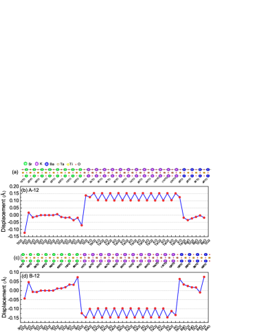
For our computational investigation, we set the thickness of STO layer to 8 uc to effectively simulate the STO substrate, and use 4 uc for the BTO capping layer. In contrast, we vary the thickness of KTO layer ( in uc) to consider different thickness of KTO layer. The structure of the central 3 uc in the STO layer is fixed at the STO bulk to reflect the bulk behavior in the interior of the STO substrate. The 20 Å of vacuum is enough to avoid artificial effects in the slab model. We use A- to denote the A-type STO/KTO()/BTO heterostructure with the thickness uc for the KTO layer, and take B- for the B-type one. At the STO/KTO interface, the STO layer is terminated with SrO AL and the KTO layer with TaO2 AL for the A- heterostructure, the STO layer is terminated with TiO2 AL and the KTO layer with KO AL for the B- heterostructure. Accordingly, the KTO/BTO interface is KO/TiO2 (top BTO surface is a BaO AL), and TaO2/BaO (top BTO surface is a TiO2 AL), respectively. These will make big differences in electronic properties. We have completed structural optimization with = 4, 6, 8, 10, and 12 uc.
The optimized atomic structures for A-12 and B-12 heterostructures are shown in Figs. 1(a) and 1(c), respectively. To show their structural features, we present the AL-resolved out-of-plane cation displacements with respect to the centers of the nearest O anions in Figs. 1(b) and 1(d) for A- and B-12 heterostructures, respectively. In the KTO layer, the value of displacement is positive for A-12 heterostructure, but negative for B-12 heterostructure. We also calculate spontaneous polarization of optimized tetragonal bulk KTO with the in-plane lattice constants set to 3.905Å, obtaining 50 C/cm2 (0.476, where is electron charge), which means a ferroelectric phase for stressed KTOadd5 . These imply that within the KTO layer, the displacement can reflect out-of-plane polarization and the opposite values between the A-12 and B-12 are caused by the two different types of atomic terminations. Moreover, when resolved to ALs in the KTO, the absolute displacement for the KO AL is less than that for the TaO2 AL, . It is noticed that the displacements in KTO thin film is substantially larger than those in STO and BTO layers, which implies that spontaneous polarization is very small in the BTO and STO layers. This is consistent with the intrinsic nonpolar state in STO and the stabilized nonpolarized state of BTO thin film under 5 nmfredrickson2015switchable . On the other hand, there are some noticeable displacements at the STO or BTO side of the interfaces, which can be attributed to interfacial effects, and the displacements of the KTO layer becomes smaller at the interfaces, indicating that the polar discontinuity caused by polar (KTO)/nonpolar (STO, BTO) interface is reduced by the structural distortion. For the other values, we obtain similar structural features.
III.2 Interfacial 2D electron and hole gases
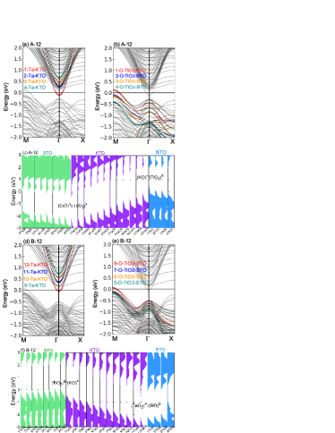
To display the electronic properties of the A-12 and B-12 heterostructures, we plot the orbital-resolved band structures and AL-resolved density of states (DOS) in Fig. 2. The effect of the KTO thickness on electronic bands of the STO/KTO/BTO heterostructure is presented in Fig. S1 and S2 (supporting information). It is clear that there exists an insulator-to-metal transition at for both the A-type and B-type cases. It is insulating for and metallic for and 12. The electronic band structures are calculated along M (, ) (, ) X (0, ) direction, and the DOS plots the sum of orbital contributions from B (B = Ti, Ta) atom and O atom of the BO2 ALs across the systems. We must notice an attractive feature that for the A- and B- heterostructures in metallic states, across the Fermi level are only the valence band maximum (VBM) at the point and the conduction band minimum (CBM) at point, similar to some electronic states in ultrathin KTO films. More interestingly, they are located at the different interfaces in the real space. These remain true for both A-type and B-type heterostructures. This is distinctively different from the STO system, where a multiband electronic structure was obtained for the 2DEG at surfaces or interfaces2014mixed .
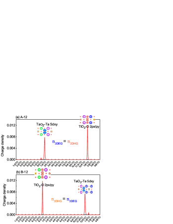
Combining the orbital-resolved band structures with the AL-resolved DOS in Fig. 2, the occupied state in the CBM is from the Ta- orbital of the (SrO)0/(TaO2)+ (STO/KTO) interface for A-type or the (TaO2)+/(BO)0 (KTO/BTO) interface for B-type; and the unoccupied state in the VBM is mostly from the O- orbitals of the TiO2 AL at the (KO)-/(TiO2)0 (KTO/BTO) interface for A-type or the (TiO2)0/(KO)- (STO/KTO) interface for B-type. Concretely, for the A-12 heterostructure, the electrons transferred from the VBM states at the STO/KTO interface are captured by the CBM (creating electron carriers) at the KTO/BTO interface, which results in unoccupied O- VBM states (creating holes) at the KTO/BTO interface. For the B-12 heterostructure, the electron carriers are contributed by the CBM states at the KTO/BTO interface and the hole carriers result from the empty VBM states at the STO/KTO interface. This implies that a pair of 2D electron and hole gases is formed at the two interfaces in the STO/KTO/BTO heterostructures. These are presented in Fig. 3, which indicates that the electron and hole carriers are highly confined to in-plane conduction at the interfaces, making a 2D electron gas (2DEG) and a 2D hole gas (2DHG). The electron carriers are separated from the hole carriers by the KTO layer, and the 2D electron concentration is equal to the 2D hole concentration, keeping the electric neutrality over the heterostructures.
For KTO(001) thin films, there are large Rashba energy splitting due to the spin-orbit coupling (SOC) in Ta-5dxz and 5dyz bands, but the SOC has little effect on Ta-5dxy bandszhang2019unusual ; add2 . Here, the 2DEG consists of Ta-5dxy states and the 2DHG O-2px/py states, and therefore the SOC effect is little on electronic structures of the 2DEG and 2DHG. Effective carrier mass () is an important parameter. It can be evaluated from the band dispersion, xia2018universality ( is Planck’s constant and describes the band). For our cases, the effective electron mass at point is ( is the mass of the free electron). This is in excellent agreement with experimental value for the KTO surface 2DEG measured by ARPES2012subband and nearly half that of a surface 2DEG on STO2011creation . Moreover, the effective hole masse is anisotropic. For A-12, is along the direction and along the direction. For B-12, is along the direction and along the direction. The hole effective masses at point for A-12 and B-12 are similar with the hole effective mass of found for STO/LAO/STO structurelee2018direct . Our calculation shows that the carrier concentration values of the 2DEG and 2DHG are cm-2 (0.059) for A-12, and cm-2 (0.034) for B-12.
III.3 Electrostatic potentials and electric field trend
The monolayer-resolved planar averaged electrostatic potentials of the optimized A-12 and B-12 heterostructures are shown (black solid lines) in Figs. 4(a) and 4(c), respectively. To better elucidate the oscillating curves, they are further averaged along the z directionadd1 , resulting in the smooth curves (red solid lines) in Figs. 4(a) and 4(c). For comparison, we also plot the corresponding curves (blue dash lines) before optimization (without relaxation). The most important feature is the opposite slope inside the KTO layer between the A-12 and B-12 heterostructures. For the A-12 in Fig. 4(a), there exists an ascendent slope in the electrostatic potential across the KTO layer from the (SrO)0/(TaO2)+ (STO/KTO) interface to the (KO)-/(TiO2)0 (KTO/BTO) interface, whereas for the B-12 in Fig. 4(c), a descendent slope in the electrostatic potential across the KTO layer from the (TiO2)0/(KO)- (STO/KTO) interface to the (TaO2)+/(BaO)0 (KTO/BTO) interface. This distinctive feature can be explained by observing that the electrostatic potential always increases from the (TaO2)+ end to the (KO)- end of the polar KTO layer sandwiched in both A-type and B-type heterostructures.
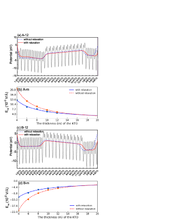
Furthermore, we can estimate an effective electric field by calculating the slope of further-averaged electrostatic potential. In order to elucidate the evolution trend of the electronic structure with the thickness of the KTO layer, we present the intrinsic electric field of the KTO film as a function of the KTO thickness in Figs. 4(b) and 4(d) for the A- and B- heterostructures, respectively, where is determined by the slope of the further-averaged electrostatic potential as a smooth curve and its direction is from the (TaO2)+ to (KO)- end. The calculated results have two distinctive features. On one hand, the structural relaxation makes the absolute value become obviously lower because it modifies the polar discontinuity at the interfaces and the stress-induced polarization within the KTO layer. For the A-12 heterostructure in Fig. 4(a), reduces from V/Å without structural relaxation to V/Å with structural relaxation; and for the B-12 in Fig. 4(b), decreases from V/Å to V/Å accordingly. On the other hand, for both the A- and B-, the absolute value of intrinsic electric field, , decreases with the thickness increasing. This trend can be explained by observing that the larger is, the smaller the polar discontinuity at the interfaces is made by structural relaxation. In detail, for the A- heterostructures in Fig. 4(b), with structural relaxation decreases with , reducing from V/Å for to V/Å for . For the B- in Fig. 4(d), with relaxation decreases from V/Å for to V/Å for , which are all comparable to electric fields detected from KTO films at the stoichiometric KTO/KMF3 (M=Zn, Ni) superlattice2020oxyfluoride .
It is very interesting that the intrinsic electric field () data for , as a function of the thickness of the KTO (), can be well fitted with a simple function with two parameters and ,
| (1) |
for both of the A- and B- STO/KTO/BTO heterostructures. The fitting parameters are summarized in Table 1. It is noticeable that for both of the types the absolute value of for the optimized case, , is smaller than that of the case without relaxation, , and accordingly the exponent is also smaller than . We also extrapolate it to uc in Figs, 4(b) and 4(d). Thus, the expression (1) implies that will become little when is very large. These mean that the intrinsic electric field originates from the interfacial effect, and then the electrostatic potential difference between the two interfaces will be saturated when the KTO thickness is large. These trends imply that the structural optimization (including interfacial relaxation) makes us avoid any divergence (polar catastrophenakagawa2006some ) due to the polarity of the KTO layer.
| Type | ||||
|---|---|---|---|---|
| A | 47.65 | 0.925 | 116.66 | 1.237 |
| B | -39.00 | 0.876 | -123.35 | 1.275 |
III.4 Aligned band diagrams towards applications
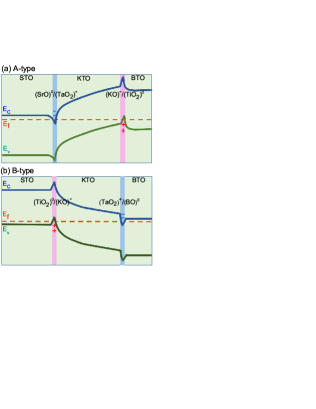
Combining all together, we show the aligned band diagrams of the A-type and B-type STO/KTO/BTO heterostructures in Fig. 5. The most standing-out feature is that there is a substantial energy band bending over the KTO layer and there exists a pair of highly-confined 2DEG and 2DHG at the interfaces for both of the heterostructures. The left-side STO/KTO [the right-side KTO/BTO] interface consists of (SrO)0/(TaO2)+ [ (KO)-/(TiO2)0 ] for the A-type heterostructure, and the interfaces consist of (TiO2)0/(KO)- and (TaO2)+/(BO)0, respectively, for the B-type. It is remarkable that the band bending of the conduction band edge brings the conduction band on the KTO side below the Fermi level and that of the valence band edge brings the valence band on the BTO or STO side above the Fermi level. As we pointed out, the KTO thickness is a key parameter and with uc ( uc as given above) there exist 2DEG and 2DHG at the interfaces for both A-type and B-type STO/KTO/BTO heterostructures. Our analysis indicates that the 2D carrier concentration () increases with monotonously, reaching a saturation value in the order of cm-2 in the large- limit.
The band bending due to the intrinsic electric field can be attributed mainly to two origins, namely the polar discontinuity at the interfaces (the divergence is avoided effectively) nakagawa2006some and the biaxial-stress-induced electric polarization within the KTO layer (the in-plane is set to and the z-axis lattice constant is optimized)Zhang2018Strain . The polar discontinuity at the interface including (TaO2)+ causes a surface charge 0.5 at most, and the polarization within the KTO layer can contribute at most -0.476 at the interface, but actually they are both renormalized by the structural optimization and electron reconstruction. Consequently, for A-12 (B-12) the electron carrier concentration of 2DEG is 0.059 (0.034), in the order of the ’ideal’ value 0.024. It is similar at the corresponding hole-hosting interfaces and in the cases of other thicknesses. Naturally, the band bending can be manipulated by applying a gating field, and such an external field can also modify the critical thickness and the 2D carrier concentrations.
Because there are no dopants in both of the STO/KTO/BTO heterostructures, there is no defect scattering for the effective carriers of the 2DEG and 2DHG. Since the electron carriers of the 2DEG originate from Ta-5dxy and the hole carriers of the 2DHG from O-2px/py, inter-band scattering is also minimized. Furthermore, inter-carrier interaction should be small because the 2D carrier concentrations are in the order of cm-2. Fortunately, these are favorable for enhancing the carrier mobility. It is expected that the 2D carrier concentrations can be controlled by applying a gating field, and thus these pairs of 2DEG and 2DHG could be useful for electronic and optoelectronic device applications such as novel transistors and sensorsadd4 . On the other hand, some spontaneous inter-interface excitons can be formed, with their life-time manipulated by applying a gating field or changing the thickness of the intermediate KTO layer, and interesting Bose-Eistein condensation could be observed in such exciton systems. If the 2DEG and 2DHG are both made superconducting2021two ; chen2021electric , some exciting effects and devices could be realized. Hopefully, these KTO-sandwiching systems could stimulate more exploration for new phenomena and novel devices.
IV Conclusion
In summary, through first-principles investigation and analysis, we have found two types of coexisting 2DEG and 2DHG at the interfaces in undoped STO/KTO/BTO heterostructures, with the surfaces insulating, when the KTO thickness reaches a crititcal value . The two interfaces consist of (SrO)0/(TaO2)+ and (KO)-/(TiO2)0 for the A-type, and (TiO2)0/(KO)- and (TaO2)+/(BO)0 for the B-type. The 2D electron carriers originate from Ta- states at the interface including TaO2 AL, and the hole carriers from O- orbitals at the other interface. The electron effective mass is 0.3, and the hole effective mass ranges from 1.06 to 1.12. The carriers are highly confined at the corresponding interfaces, and the 2D carrier concentrations are in the order of cm-2. The interfacial 2DEG and 2DHG are especially interesting because STO, KTO, and BTO bulks are insulating. Our analysis indicates that the polar discontinuity at the interfaces including the (TaO2)+ and (KO)- causes global structural optimization and partial electron reconstruction over the KTO layer in order to avoid electrostatic divergence, and on the other hand pins the direction of stress-induced electric polarization within the KTO layer, and consequently the 2DEG and 2DHG are simultaneously formed at the interfaces because of the band bending due to the intrinsic electric field effects in the KTO layer. These interfacial 2DEG and 2DHG could stimulate more exploration for more sandwich heterostructures, new phenomena, and novel devices.
Acknowledgements.
This work is supported by the Nature Science Foundation of China (Grant Nos.11974393 and 11574366) and the Strategic Priority Research Program of the Chinese Academy of Sciences (Grant No. XDB33020100). All the numerical calculations were performed in the Milky Way #2 Supercomputer system at the National Supercomputer Center of Guangzhou, Guangzhou, China.References
- (1) A. Ohtomo and H. Y. Hwang, Nature 427, 423 (2004)
- (2) N. Nakagawa, H. Y. Hwang, and D. A. Muller, Nat. Mater. 5, 204 (2006)
- (3) H. Lee, N. Campbell, J. Lee, T. Asel, T. Paudel, H. Zhou, J. Lee, B. Noesges, J. Seo, B. Park, L. J. Brillson, S. H. Oh, E. Y. Tsymbal, M. S. Rzchowski, and C. B. Eom, Nat. Mater. 17, 231 (2018)
- (4) A. J. Millis and D. G. Schlom, Phys. Rev. B 82, 073101 (2010)
- (5) W.-K. Tse and S. Das Sarma, Phys. Rev. B 75, 045333 (2007)
- (6) J. P. Eisenstein and A. H. MacDonald, Nature 432, 691 (2004)
- (7) M. Basletic, J.-L. Maurice, C. Carrétéro, G. Herranz, O. Copie, M. Bibes, É. Jacquet, K. Bouzehouane, S. Fusil, and A. Barthélémy, Nat. Mater. 7, 621 (2008)
- (8) K. V. Shanavas, Phys. Rev. B 93, 045108 (2016)
- (9) W. Siemons, G. Koster, H. Yamamoto, W. A. Harrison, G. Lucovsky, T. H. Geballe, D. H. A. Blank, and M. R. Beasley, Phys. Rev. Lett. 98, 196802 (2007)
- (10) G. Khalsa and A. H. MacDonald, Phys. Rev. B 86, 125121 (2012)
- (11) M. Takizawa, H. Wadati, K. Tanaka, M. Hashimoto, T. Yoshida, A. Fujimori, A. Chikamatsu, H. Kumigashira, M. Oshima, K. Shibuya, T. Ohnishi, M. Lippmaa, M. Kawasaki, H. Koinuma, S. Okamoto, and A. Millis, Phys. Rev. Lett. 97, 057601 (2006)
- (12) S. Okamoto, A. J. Millis, and N. A. Spaldin, Phys. Rev. Lett. 97, 056802 (2006)
- (13) R. Pentcheva and W. E. Pickett, Phys. Rev. Lett. 102, 107602 (2009)
- (14) H. Zhang, X. Yan, X. Zhang, S. Wang, C. Xiong, H. Zhang, S. Qi, J. Zhang, F. Han, N. Wu, B. Liu, Y. Chen, B. Shen, and J. Sun, Acs Nano 13, 609 (2019)
- (15) L. M. Vicente-Arche, J. Bréhin, S. Varotto, M. Cosset-Cheneau, S. Mallik, R. Salazar, P. Noël, D. C. Vaz, F. Trier, S. Bhattacharya, A. Sander, P. Le Févre, F. Bertran, G. Saiz, G. Ménard, N. Bergeal, A. Barthélémy, H. Li, C.-C. Lin, D. E. Nikonov, I. A. Young, J. E. Rault, L. Vila, J.-P. Attané, and M. Bibes, Adv. Mater. 33, 2102102 (2021)
- (16) H. Zhang, Y. Ma, H. Zhang, X. Chen, S. Wang, G. Li, Y. Yun, X. Yan, Y. Chen, F. Hu, J. Cai, B. Shen, W. Han, and J. Sun, Nano Lett. 19, 1605 (2019)
- (17) H. Zhang, Y. Yun, X. Zhang, H. Zhang, Y. Ma, X. Yan, F. Wang, G. Li, R. Li, T. Khan, Y. Chen, W. Liu, F. Hu, B. Liu, B. Shen, W. Han, and J. Sun, Phys. Rev. Lett. 121, 116803 (2018)
- (18) Y. Sun, Y. Liu, S. Hong, Z. Chen, M. Zhang, and Y. Xie, Phys. Rev. Lett. 127, 086804 (2021)
- (19) C. Liu, X. Yan, D. Jin, Y. Ma, H.-W. Hsiao, Y. Lin, T. M. Bretz-Sullivan, X. Zhou, J. Pearson, B. Fisher, J. S. Jiang, W. Han, J.-M. Zuo, J. Wen, D. D. Fong, J. Sun, H. Zhou, and A. Bhattacharya, Science 371, 716 (2021)
- (20) Z. Chen, Z. Liu, Y. Sun, X. Chen, Y. Liu, H. Zhang, H. Li, M. Zhang, S. Hong, T. Ren, C. Zhang, H. Tian, Y. Zhou, J. Sun, and Y. Xie, Phys. Rev. Lett. 126, 026802 (2021)
- (21) Y. Ma, J. Niu, W. Xing, Y. Yao, R. Cai, J. Sun, X. Xie, X. Lin, and W. Han, Chin. Phys. Lett. 37, 117401 (2020)
- (22) Z. Chen, Y. Liu, H. Zhang, Z. Liu, H. Tian, Y. Sun, M. Zhang, Y. Zhou, J. Sun, and Y. Xie, Science 372, 721 (2021)
- (23) A. Gupta, Harsha, A. Kumari, M. Dumen, S. Goyal, R. Tomar, N. Wadehra, P. Ayyub, and S. Chakraverty, Advanced Materials 34, First published on 27 December 2021, https://doi.org/10.1002/adma.202106481 (2022)
- (24) P. D. C. King, R. H. He, T. Eknapakul, P. Buaphet, S.-K. Mo, Y. Kaneko, S. Harashima, Y. Hikita, M. S. Bahramy, C. Bell, Z. Hussain, Y. Tokura, Z.-X. Shen, H. Y. Hwang, F. Baumberger, and W. Meevasana, Phys. Rev. Lett. 108, 117602 (2012)
- (25) X. Zhao and A. Selloni, Phys. Rev. Mater. 3, 015801 (2019)
- (26) M. Setvin, M. Reticcioli, F. Poelzleitner, J. Hulva, M. Schmid, L. A. Boatner, C. Franchini, and U. Diebold, Science 359, 572 (2018)
- (27) G. Kresse and D. Joubert, Phys. Rev. B 59, 1758 (1999)
- (28) P. E. Blöchl, Phys. Rev. B 50, 17953 (1994)
- (29) J. P. Perdew, K. Burke, and M. Ernzerhof, Phys. Rev. Lett 77, 3865 (1996)
- (30) J. P. Perdew, A. Ruzsinszky, G. I. Csonka, O. A. Vydrov, G. E. Scuseria, L. A. Constantin, X. Zhou, and K. Burke, Phys. Rev. Lett 100, 136406 (2008)
- (31) V. I. Anisimov, F. Aryasetiawan, and A. Lichtenstein, J. Phys.: Condens. Matter 9, 767 (1997)
- (32) X.-J. Zhang and B.-G. Liu, Phys. Chem. Chem. Phys. 20, 24257 (2018)
- (33) S. Okamoto, A. J. Millis, and N. A. Spaldin, Phys. Rev. Lett. 97, 056802 (2006)
- (34) H. Uwe, H. Unoki, Y. Fujil, and T. Sakudo, Solid State Commun. 13, 737 (1973)
- (35) K. D. Fredrickson and A. A. Demkov, Phys. Rev. B 91, 115126 (2015)
- (36) N. C. Plumb, M. Salluzzo, E. Razzoli, M. Månsson, M. Falub, J. Krempasky, C. E. Matt, J. Chang, M. Schulte, J. Braun, H. Ebert, J. Minár, B. Delley, K.-J. Zhou, T. Schmitt, M. Shi, J. Mesot, L. Patthey, and M. Radović, Phys. Rev. Lett. 113, 086801 (2014)
- (37) N. Wu, X.-J. Zhang, and B.-G. Liu, RSC Adv. 10, 44088 (2020)
- (38) C. Xia, W. Xiong, J. Du, T. Wang, Y. Peng, and J. Li, Phys. Rev. B 98, 165424 (2018)
- (39) W. Meevasana, P. King, R. He, S. Mo, M. Hashimoto, A. Tamai, P. Songsiriritthigul, F. Baumberger, and Z. Shen, Nat. Mater. 10, 114 (2011)
- (40) A. Baldereschi, S. Baroni, and R. Resta, Phys. Rev. Lett. 61, 734 (1988)
- (41) A. C. Garcia-Castro, P. Ghosez, E. Bousquet, and A. H. Romero, Phys. Rev. B 102, 235140 (2020)