Non-linear Hybrid Surface-defect States In Defective Bi2Se3
Abstract
Surface-states of topological insulators are assumed to be robust against non-magnetic defects in the crystal. However, recent theoretical models and experiments indicate that even non-magnetic defects can perturb these states. Our first-principles calculations demonstrate that the presence of Se vacancies in Bi2Se3, has a greater impact than a mere n-doping of the structure, which would just shift the Fermi level relative to the Dirac point. We observe the emergence of a non-linear band pinned near the Fermi level, while the Dirac cone shifts deeper into the valence band. We attribute these features in the bandstructure to the interaction between the surface and defect states, with the resulting hybridization between these states itself depending on the position and symmetry of the Se vacancy relative to the surfaces. Our results bring us a step closer to understanding the exotic physics emerging from defects in Bi2Se3 that remained unexplored in prior studies.
keywords:
topological insulators, surface states, vacancy defects1 Introduction
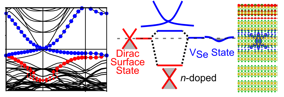
Topological insulators are a new class of materials with a gapped bulk and metallic surfaces (for 3D materials) or edges (for 2D materials) 1, 2. These surface states are topologically non-trivial, and originate from the strong spin-orbit coupling that preserves time-reversal symmetry. They are known to be robust against defects, strain and disorder, assuming that the perturbation is modest enough to preserve the original character of the material. Since these surface states exhibit Dirac fermion behavior (linear dispersion), not only are they being explored for applications in quantum computing and spintronics, but their topological protection allows one to test and explore exotic and fundamental concepts in physics, such as Majorana particles 3 and magnetic monopoles 4. As different proposed applications of topological insulators depend on the assumption of a linear Dirac cone, it is critical to understand if the surface states indeed remain unperturbed, or if they are reshaped by the non-magnetic defects, and to what extent. In fact, a recent theoretical model and experiments 5, 6, 7 indicate that the latter is indeed the case. However, earlier first-principles calculations 8, 9 of these defects did not consider the reshaping of the surface states due to their interactions with defect states.
Amongst the bismuth selenide family of compounds (Bi2Se3, Sb2Te3 and Bi2Te3), Bi2Se3 10, 11 is the most widely studied 3D topological insulator, with a large bulk-band gap of 0.3 eV. Selenium vacancies (VSe) are known to be a common defect in Bi2Se3, and are assumed to be responsible for the n-type doping of the as-grown crystals 12, 13. Due to high volatility of selenium 14, formation of additional vacancies on the surface of cleaved Bi2Se3 slabs is expected. This is possibly responsible for the observed aging of the slabs, as they show changes in electronic properties with time 15, 16. Though a vast literature exists on the formation energy of Se vacancies in Bi2Se3 17, 18, 8, 9, 19, very little is discussed about the nature of the defect states, their placement in the electronic band structure and the effect of their positions on the properties of Bi2Se3 surface states. Furthermore, most theoretical works have either considered very large densities of vacancies, such as a surface termination with all top selenium atoms removed, or symmetric defects on both surfaces that preserve the inversion symmetry of the slab 8. Hence, the effect(s) of lower concentrations of vacancies on Bi2Se3 remain unknown. To address these important questions, we carry out a detailed analysis on the effect of Se vacancies on the Dirac cone of the Bi2Se3 slabs, explore the coupling between the surface and defect bands, and their emergent signature in the band structure and STM images.
2 Computational Details
SIESTA (Spanish Initiative for Electronic Simulations with Thousands of Atoms) package 20, 21 was used to carry out the Density Functional Theoretical (DFT) calculations. A plane wave mesh cutoff of 300 Ry was used for non-spin polarized calculations, whereas a lower cutoff of 150 Ry was used for calculations including spin-orbit interactions. The electron-ion interactions were modeled with fully-relativistic norm-conserving pseudopotentials obtained from PseudoDojo 22, 23, with exchange correlation energy between electrons approximated by the GGA functional parameterized by Perdew-Burke-Ernzerhof (PBE)24. A double zeta polarized basis set was used in our calculations. The Brillouin Zone (BZ) integrations were carried out over a Monkhorst Pack k-point mesh of size 666 for primitive bulk cell and 661 for slab of size 11nQL, where nQL stands for the number of quintuple layers (QL). Defects were created in supercell slabs of sizes 666 QL and 557 QL. Only BZ center integrations were carried out for the defective supercells.
The bulk primitive cell was relaxed (including spin-orbit coupling) till the Hellman-Feynman forces on the atoms were <0.01 eV/Å and the stress components in each direction were <0.001 eV/ Å3. This relaxed bulk structure was used to create 11nQL (nQL = 6, 7) slabs, which was further relaxed (atoms only, with spin-orbit coupling) until the Hellman-Feynman forces on the atoms were <0.01 eV/Å. This slab structure was then periodically repeated in the in-plane lattice directions to generate the 666 QL (1080 atoms) and 557 QL (875 atoms) supercell slabs. To estimate the structural relaxation due to Se vacancy defects, we carried out non-spin polarized calculations on the defective supercell slabs and the atoms were allowed to relax till the Hellman-Feynman forces on the atoms were <0.04 eV/Å. In addition, we kept the Bi atoms fixed in their respective planes (allowed to move in-plane), to fix the interplanar spacing of the layers to that of bulk. Because we exclude the spin-orbit effects in the relaxation calculations, we keep the Bi atoms fixed in their respective planes (allowed to move in-plane) since GGA parameterization overestimates the interplanar spacing (a known drawback). This constraint is reasonable since it mimicks experimental slabs, where the defect concentration is approximately two orders of magnitude lower than in our calculations depending on the quality of the sample, and would not affect the bulk interplanar spacing significantly. A vacuum of 24 Å was included in the non-periodic direction to minimize the interaction between the periodic images.

3 Results & Discussion
3.1 Vacancy configurations
Bulk Bi2Se3 has R-3m (#166) space group symmetry with a) Bi at Wyckoff position 6c (0,0,0.3985), and b) Se with two symmetry inequivalent Wyckoff positions, 3a (0,0,0) and 6c (0,0,0.2115); and lattice constants a = b = 4.19 Å and c = 28.63 Å25. It is a layered material with each layer containing 5 atoms (a formula unit), and therefore known as a quintuple layer (QL). The QLs have -A-B-C- stacking along the ‘z (c)’ direction. The DFT estimates of lattice constants for the 11nQL (nQL = 6 and 7) cell are a = b = 4.21 Å i.e. overestimation by 0.4% from the experimental value. Whereas the estimated bulk lattice parameter, c = 28.92 Å is overestimated from the experimental value by 1%, well within the limits of DFT errors. Due to the difference between the electronic topology of the bulk with respect to vacuum, cleaving the bulk into a slab gives rise to topologically protected Dirac surface states at the Fermi level, assuming the slab is thick enough to reduce interaction between top and bottom surfaces. For slabs with nQL 6, we find that the surface states become almost degenerate (i.e. produce a Dirac cone) at the Fermi level with a negligible gap between the conduction and valence band Dirac cones ( 1 meV.Pertsova et al. 26 have shown that this gap essentially goes to zero for 40 QLs, which is when the top and bottom surface states become decoupled.
We construct 666 QLs and 557 QLs slabs to study the effects of Se vacancy defects on the surface states, with the 2 slabs representing different in-plane defect densities. In the 666 QLs slabs, we create single VSe defects that break the inversion symmetry of the slab, capturing the defect- and substrate-induced asymmetry in experimental samples27. On the other hand, in the 557 QLs slabs, we create pairs of VSe defects that conserve the inversion symmetry of the top and the bottom QL layers, allowing for a direct comparison with the existing literature8. A comparison of results for the 666 QLs and 557 QLs slabs also allows us to highlight and differentiate between the effects of inversion symmetry breaking on the bandstructure and those due to defects themselves. As the overall results for the two structures are qualitatively similar, those for the 557 QLs slab are discussed in the Supporting Information, S2. In both the 666 QLs and 557 QLs slabs, we create Se vacancies at the symmetry-inequivalent Wyckoff positions (3a and 6c) at the surface and in the interior (i.e. bulk) of the slab. Since the surface breaks the symmetry between the two Se atoms at 6c, we distinguish them as Se1 on the surface and Se1' below the surface (interface of topmost and next QL). Se2 is the Se atom at the 3a site which is sandwiched between two BiSe layers (see Figure 1A). We will henceforth refer to vacancies in the surface (bulk) QL with a subscript ‘s’(‘b’). An Se vacancy in a 666 QLs slab corresponds to a defect concentration of 1019 cm-3 (in-plane concentration = 2.6 1013 cm-2), comparable to the values reported in experiments28, 17, which range from 1011 to 1020 cm-3. We note that, previous theory works 8, 9 simulated a single Se vacancy per 33 in-plane supercell, while we use 66 and 55 in-plane supercells. The small supercell size in the earlier works results in stronger interactions between the periodic images of the vacancies, changing the effect of the defect states on the topological surface states of Bi2Se3. The band structure of a pristine 666 QLs slab is shown in Figure 1 B, and shows the Dirac cone at the Fermi level.
3.2 Bulk vacancies

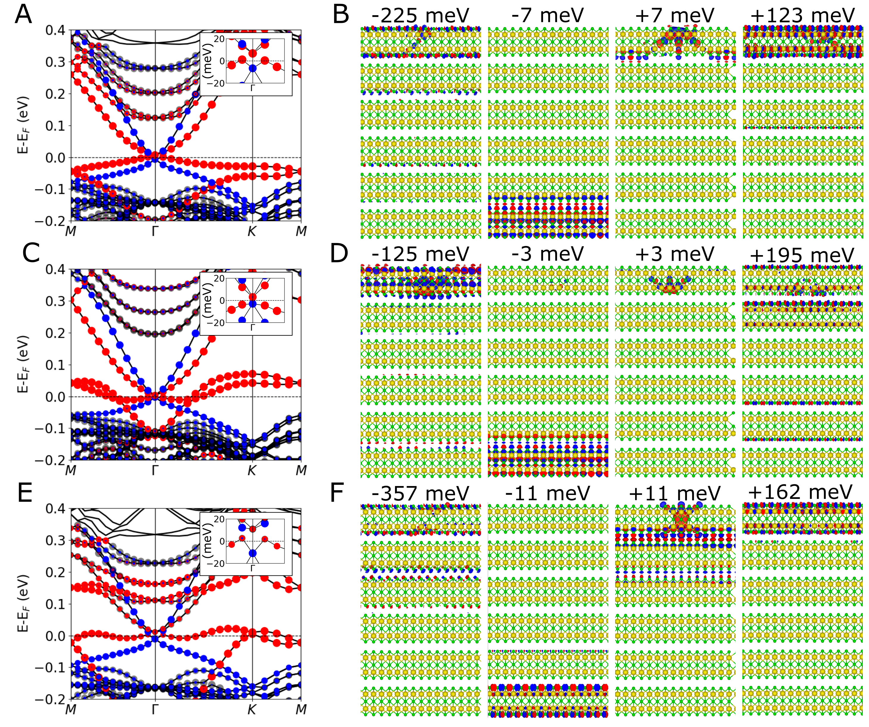
We first explore how the vacancies in the bulk of the Bi2Se3 slab modify its electronic structure properties. The bandstructures for the two inequivalent defects, VSe1b and VSe2b, are plotted in Figures 2 A and C, respectively. The contributions of the top (bottom) surface (QL) to the electronic states are drawn with red (blue) circles; black circles represent the contribution of the bulk. Note that the states at the and M points in the Brillouin Zone (BZ) are doubly degenerate, due to their topological nature. The defect breaks the structure inversion symmetry (SIA) of the slab 29, with the top QL being closer to the defect. This lifts the degeneracy of the surface states localized on the top and bottom surfaces, with the top surface state moving lower in energy due to its larger interaction with the defect.29, 27 The Dirac cones associated with the top surface states are shifted by -42 meV and -133 meV below Fermi level for VSe1b and VSe2b, respectively. In contrast, for the inversion-symmetry conserving VSe2b in 557 QLs slab (see Figure S2 C), both the Dirac cones are degenerate due to conservation of inversion symmetry. The shift of the Dirac point below the Fermi level, which is due to interaction of the surface states with the defect 5, 6, 30, (discussed later in detail) likely depends on the distance of the defect from the surface, and is expected to be reduced for defects that are much farther away from the surfaces in thicker slabs.
Figures 2 B and D show the wavefunctions at the Dirac points (i.e. -point) for the two bulk defects. In the case of VSe1b, we find that the topological character (linear dispersion) for the top and bottom surface states is preserved, with the associated Dirac cones shifted below the Fermi level by about -42 meV and -10 meV (see Figure 2 B, left-most and middle panels). Figure 2 B (right-most panel) also shows that the unoccupied conduction band minimum at . It is about +11 meV above the Fermi level, and is mostly localized around the defect site. Interestingly, the wavefunctions at about -42 meV and a lower isosurface plot of the state at about +11 meV show that they are actually admixtures of the top surface states and defect states, being bonding and anti-bonding states, respectively. In the case of the bulk defect, VSe2b, the top surface state is shifted by -133 meV, whereas the bottom surface state at -27 meV is localized to the bottommost QL. Unlike the hybridization between surface and defect states seen for VSe1b, the defect-state associated with VSe2b is decoupled from the surface states (see Figure 2 D at -133 meV and -27 meV). Anti-crossing of the surface states and the defect band (see Figure 2 C at +0.05 eV) confirms their decoupling. This shows that although the VSe2b defect is at a similar distance from both the surfaces as VSe1b, the Wyckoff position of the Se vacancy in bulk, affects the electronic structure properties of a Bi2Se3-slab differently. In part, these differences might stem from the fact that a VSe2 defect preserves the intra-layer inversion symmetry as opposed to VSe1, which breaks it. We find similar behavior in the 557 QLs slab with VSe2b (see Figure S3).
3.3 Surface vacancies
Unlike bulk Se vacancies, where the interaction between the defect and surface states can be reduced by considering thicker slabs, surface vacancies merely by virtue of their position are inherently coupled to the surface states. For the surface defects VSe1s, VSe1s' and VSe2s, the calculated band structure clearly shows strong interactions with the topological surface states (see Figures 3 A, C and E), and the emergence of a non-linear (almost parabolic) band at the Fermi level (that was missing in for bulk vacancies). In addition, the top QL state shifts much deeper into the valence band as compared to that in the presence of bulk defects (see Figure S6 for band structure plotted for wider energy range). Following the signatures of the top QL contribution to the band structure (colored red in Figure 3, left column) into the valence band, we identify these surface states by plotting the charge densities of their wavefunctions at -point (see left-most column in Figure 3 B, D and F). The surface states of the defective top QL are shifted by -225 meV, -125 meV and -357 meV for VSe1s, VSe1s' and VSe2s, respectively. Not only are they localized to the topmost QL, but they also exhibit linear dispersion in the band structure (see Figure S6), with the same Dirac cone features as in a pristine slab (see Figure 1 B). In each of these Dirac cones that are found much deeper in the valence band, the lower branch of the cone shows the expected upward dispersion, which arises from the term in the Dresselhaus spin-orbit coupling 31. This further confirms the topological protection of surface states in Bi2Se3, even in the presence of a considerably large in-plane concentration of Se vacancies at the surface.
Furthermore, we see a shift of the Dirac cone from the bottom (pristine) layer (see Figure 3, band structure in blue and second panel of the wavefunctions) below the Fermi level by -7, -3 and -11 meV for VSe1s, VSe1s', VSe2s, respectively. The downward shift from the Fermi level is a result of the inter-surface coupling between the defect and bottom QL 29,. This is confirmed from the smaller shift of -5 meV for a single surface vacancy in the 557 QLs slab (see Figure S5, and an equal and opposite shift seen in the hybrid, mostly defect-type, state around -point (Figures 3 B, D and F, third panel). We expect the shift to reduce with increasing slab thickness. Interestingly, we also find that the top part of the surface state cone from the top QL surface has shifted into the conduction band by 123 and 162 meV for VSe1s and VSe2s, respectively (Figures 3 B, D and F, right-most panel). On the other hand, the surface state at 195 meV for VSe1s' shows greater delocalization, with significant contributions from the next QL due to hybridization with the bulk conduction band states. The splitting of the top and bottom part of the surface state Dirac cone agrees with the work of Black-Schraffer et al.32.
3.4 Origin of the defect band
In addition to identifying the Dirac points associated with the top and bottom surface states, we investigate the origin of bands lying between -0.2 eV to 0.2 eV (see Figures 3 A, C and E), focusing on the non-linear bands near the Fermi level in this range. Figure 4 A is a schematic diagram depicting our proposed origin of these bands. The Se vacancy within the top QL introduces SIA,29 which lifts the degeneracy between the top (dashed yellow in Figure 4 A) and bottom QL layer (solid purple) Dirac cones. The Se1 and Se1' positions possess 3m point group symmetry, whereas the Se2 position has -3m symmetry. Here we focus our discussion on the VSe1s defect, but similar explanation is valid for VSe2s and VSe1s' as well. Due to the 3m symmetry of the VSe1s defect, the dangling 'p' orbitals of the Bi atoms (near the vacancy) split as the singly degenerate A1 and doubly degenerate E bands. The A1 defect band is near the Fermi level, whereas the E bands are higher in the conduction band at 0.8 eV (see Figure S9). On closer inspection of the conduction bands (see Figure 3 A, C and E), we find states in the bulk band gap that were absent for the pristine slab (see Figure 1 B). These states are the Quantum Well (QW) states that are induced by the band bending at vacuum and defective QL interface due to the symmetry breaking and doping of the top QL by the defect 27.
In the absence of any interaction between the defect and the surface states, the band structure would resemble Figure 4 A (lower-branch, middle plot). Interaction between the defect/QW and topologically protected top surface states 33, 32 creates hybrid bands (h1h6), shown in Figure 4 A, lower-branch, right-most plot (also see S7 for a numerical model based on 33). Here, the defect band spin-splits into two branches, one of which mixes with the lower part of the Dirac cone of the top QL. The Dirac cone that is deep in the valence band is a hybrid (h1h2) with the lower part (h1) originating from the top QL surface state, and the upper part (h2) from the defect. This mixing is evident in the charge densities of the wavefunctions (see Figures 3 B, D, F at point). h3 is the other spin-split defect band that primarily interacts with the lower part of the Dirac cone. Since the defect forms an integral part of the surface, h1, h2 and h3 also acquire some defect and surface characters, respectively. Similarly, the upper part of the original Dirac cone (of the top QL) mixes with the QW state 27 present above the Fermi level in the bulk gap region and forms, h4, h5 and h6 bands. Here, the non-linear/parabolic band (h4) above the Fermi level, is mostly defect-like in character (see Figure S10). This mixing behavior observed here is quite different from an earlier work by Seixas et al., 33 where a ‘twinning’ of the Dirac cone at the interface of a topological insulator and a trivial insulator was reported. In that case, the mixed states only emerge at the high symmetry points in the BZ. Hence, the hybridization, which results in the non-linear/parabolic band, h4, described in our work is a unique signature characterizing the Se vacancies in Bi2Se3. h1h6 also exhibit helical spin-texture (see Figure S11), being admixtures of the topologically protected surface states and defect states. Lastly, we note the interaction between the defect and the bottom QL. This shifts the defect state and the bottom surface state above and below the Fermi level, respectively. The magnitude of the shift appears to be correlated to: a) how deep the h1h2 band has shifted into the valence band, and b) screening of the vacancy by adjacent layers. The shift is larger for VSe2s in comparison with VSe1s and VSe1s', as the h1h2 hybrid band is also lower (see Figures 3 A, C and E). In the case of VSe1s', though it has similar placement in the QL as VSe1s, the screening effect of the adjacent QL for the VSe1s' makes the splitting negligibly small (see Figure S12). A quantitative analysis of the extent of the defect and surface state splitting (h1, h6 and h3, h4 separation) has been explored in a generalized theoretical model of a strong three-dimensional topological insulator by Black-Schraffer et al. 32, where they show that the magnitude of the shift of the surface states into the conduction and valence bands is dependent on the strength of the defect potential.

The h1h6 bands preserve the topological character of the surface states, i.e. they span the bulk energy gap and connect the bulk valence and conduction bands. They are similar to the so-called ‘topological dangling bond states,’34, 8 which were reported when an entire layer of Se atoms is missing from the top QL. It is important to note that the presence of surface states (h1 and h6) outside the bulk band gap region encourages scattering from the bulk states. Thus, the surface states lose their protection from spin backscattering processes. The dispersion of h2 and h3 for VSe1s' and VSe2s (between energies of -0.05 to 0.05 eV, Figures 3 C and E), gives rise to multiple Fermi surface nestings, which is similar to Bi2Se3 slabs cleaved along different planes 34. This feature allows for spin backscattering processes, previously forbidden in a pristine slab. For energies 0.05 eV, the multiple Fermi-surface nesting disappears and the spin backscattering processes again become forbidden. Thus, by controlling the position of the Fermi level via gating, one can control the surface spin current in defective Bi2Se3. This possibility opens up new applications in spintronics that can replace the existing semiconductor based devices.
It is important to note that even though the parabolic band, h4 (see Figures 3 A, C and E), looks like a 2DEG (2D electron gas) 15, 16 in Bi2Se3, its origin and spin texture reveal the opposite. h4 shows spin-momentum locking with a slight out-of-plane ‘z’ component (due to defects 35, see Figure S11), in contrast with a 2DEG which is spin-degenerate 15, 16. A 2DEG band in the topological insulators is known to originate from band bending induced by defects36 or by change in the van der Waals gap between layers 37, not hybridization. It is also formed well above the Dirac point 36, 15, 16, 37 in the conduction band. These differences lead us to believe that h4 is a previously unreported characteristic of Se vacancies in Bi2Se3. The signature of the defect is also seen as a resonant defect state above the Fermi level in the density of states (see Figure 4 B), consistent with predictions and observations 7, 5, 6, 30 in earlier works.
Our calculations for defect in the 666 QLs also confirm experimental reports of a Rashba-like splitting of the conduction band states,15 (see Figures 2, 3 and S13). This splitting is due to inversion asymmetry introduced by the asymmetric defects in 666 QLs slabs, that is absent in the symmetrically placed defects in 557 QLs slabs (see Figure S2). The exception is the VSe1s' defect, where this splitting is negligible. Although an exact explanation of the latter is outside the scope of this work, different contributing factors might include a countering of the Rashba-like splitting by the effects of local strain (due to the defect) on the bandstructure, or the screening of the defect potential (see Figure S12). Figures 4 C-E are simulated STM images (at constant height and V = +0.3 eV) for surface defects, providing their experimental signatures. We find that our STM images are in reasonable agreement with experimental observations of Dai et al.19. The differences could be due to sampling of a different energy range in our calculations.
4 Conclusions
Our detailed study of Se vacancies in Bi2Se3 shows that a neutral Se vacancy state hybridizes with the bottom part of the surface state Dirac cone and shifts it deeper into the valence band, i.e. it n-dopes the layer. On the other hand, the top part of the Dirac cone also hybridizes with the quantum well (bulk) state. The QW-defect-surface states interaction, in turn, gives rise to a non-linear (parabolic) band with primarily defect character at the Fermi level, while shifting the top Dirac cone into the conduction band. We find that the non-linear bands at the Fermi level originating at the surface prohibit spin-backscattering processes for VSe1s, just like the surface states in pristine Bi2Se3 slabs. Hence, in this structure, the directionality of the spin current at the surface is preserved. The origin, spin texture and position with respect to the Fermi level of this band is unlike the 2DEG observed in Bi2Se3 15, 16, which makes it a unique feature of surface vacancies in this material. For the first time, our DFT results confirm the presence of such a defect band consistent with earlier reports 5, 6. The unique dispersion of this band allows one to switch the spin backscattering processes ‘on/off’ by controlling its occupancy, providing additional tunability to the spin current. Deterministic placement of Se-vacancies can provide an added functionality to topological-insulator based applications in spintronics. This would be a considerable improvement over traditional semiconductor spintronic materials. Studying these defects under stress, strain, electric fields and gas contaminants would be an exciting future scope of this work.
5 Supporting Information
The Supporting Information includes results for symmetric Se vacancies in 557 QLs slab, numerical model to explain the hybridization of defect states with the topological surface states, Rashba splitting in the electronic structure, spin-momentum locking plots, and the convergence studies of the electronic structure with plane wave cutoff, displacement of Bi atoms and Hamiltonian matrix elements.
6 Acknowledgements
We would like to thank Dr. Ivan Naumov for helpful discussions and inputs, and Dr. J. R. Knab for help with copy editing. This work was supported W. M. Keck Research Foundation grant and NSF Grant number DMR-1752840. We acknowledge the computational support provided by the Extreme Science and Engineering Discovery Environment (XSEDE) under Project PHY180014, which is supported by National Science Foundation grant number ACI-1548562, and Maryland Advanced Research Computing Center.
References
- Kane and Mele 2005 Kane, C. L.; Mele, E. J. Phys. Rev. Lett. 2005, 95, 226801
- Bernevig et al. 2006 Bernevig, B. A.; Hughes, T. L.; Zhang, S.-C. Science 2006, 314, 1757–1761
- Grover et al. 2014 Grover, T.; Sheng, D. N.; Vishwanath, A. Science 2014, 344, 280–283
- Qi et al. 2009 Qi, X.-L.; Li, R.; Zang, J.; Zhang, S.-C. Science 2009, 323, 1184–1187
- Miao et al. 2018 Miao, L.; Xu, Y.; Zhang, W.; Older, D.; Breitweiser, S. A.; Kotta, E.; He, H.; Suzuki, T.; Denlinger, J. D.; Biswas, R. R.; Checkelsky, J. G.; Wu, W.; Wray, L. A. npj Quantum Materials 2018, 3, 29
- Zhong et al. 2017 Zhong, M.; Li, S.; Duan, H.-J.; Hu, L.-B.; Yang, M.; Wang, R.-Q. Scientific Reports 2017, 7, 3971
- Teague et al. 2012 Teague, M.; Chu, H.; Xiu, F.-X.; He, L.; Wang, K.-L.; Yeh, N.-C. Solid State Communications 2012, 152, 747–751
- Yan et al. 2013 Yan, B.; Zhang, D.; Felser, C. physica status solidi (RRL) – Rapid Research Letters 2013, 7, 148–150
- Wang and Zhang 2020 Wang, S.; Zhang, P. Physics Letters A 2020, 384, 126281
- Xia et al. 2009 Xia, Y.; Qian, D.; Hsieh, D.; Wray, L.; Pal, A.; Lin, H.; Bansil, A.; Grauer, D.; Hor, Y. S.; Cava, R. J.; Hasan, M. Z. Nature Physics 2009, 5, 398–402
- Zhang et al. 2009 Zhang, H.; Liu, C.-X.; Qi, X.-L.; Dai, X.; Fang, Z.; Zhang, S.-C. Nature Physics 2009, 5, 438–442
- Navrátil et al. 2004 Navrátil, J.; Horák, J.; Plecháček, T.; Kamba, S.; Lošt’ák, P.; Dyck, J.; Chen, W.; Uher, C. Journal of Solid State Chemistry 2004, 177, 1704–1712
- Jafarpisheh et al. 2021 Jafarpisheh, S.; Ju, A.; Janßen, K.; Taniguchi, T.; Watanabe, K.; Stampfer, C.; Beschoten, B. physica status solidi (b) 2021, 258, 2000021
- Kim et al. 2019 Kim, J.; Shin, E.-H.; Sharma, M. K.; Ihm, K.; Dugerjav, O.; Hwang, C.; Lee, H.; Ko, K.-T.; Park, J.-H.; Kim, M.; Kim, H.; Jung, M.-H. Scientific Reports 2019, 9, 1331
- King et al. 2011 King, P. D. C. et al. Phys. Rev. Lett. 2011, 107, 096802
- Bianchi et al. 2010 Bianchi, M.; Guan, D.; Bao, S.; Mi, J.; Iversen, B. B.; King, P. D.; Hofmann, P. Nature Communications 2010, 1, 128
- Stephen et al. 2020 Stephen, G. M.; Naumov, I.; Tyagi, S.; Vail, O. A.; DeMell, J. E.; Dreyer, M.; Butera, R. E.; Hanbicki, A. T.; Taylor, P. J.; Mayergoyz, I.; Dev, P.; Friedman, A. L. The Journal of Physical Chemistry C 2020, 124, 27082–27088
- West et al. 2012 West, D.; Sun, Y. Y.; Wang, H.; Bang, J.; Zhang, S. B. Phys. Rev. B 2012, 86, 121201
- Dai et al. 2016 Dai, J.; West, D.; Wang, X.; Wang, Y.; Kwok, D.; Cheong, S.-W.; Zhang, S. B.; Wu, W. Phys. Rev. Lett. 2016, 117, 106401
- Soler et al. 2002 Soler, J. M.; Artacho, E.; Gale, J. D.; García, A.; Junquera, J.; Ordejón, P.; Sánchez-Portal, D. Journal of Physics: Condensed Matter 2002, 14, 2745–2779
- Cuadrado and Cerdá 2012 Cuadrado, R.; Cerdá, J. I. Journal of Physics: Condensed Matter 2012, 24, 086005
- van Setten et al. 2018 van Setten, M.; Giantomassi, M.; Bousquet, E.; Verstraete, M.; Hamann, D.; Gonze, X.; Rignanese, G.-M. Computer Physics Communications 2018, 226, 39–54
- García et al. 2018 García, A.; Verstraete, M. J.; Pouillon, Y.; Junquera, J. Computer Physics Communications 2018, 227, 51–71
- Perdew et al. 1996 Perdew, J. P.; Burke, K.; Ernzerhof, M. Physical review letters 1996, 77, 3865
- Nakajima 1963 Nakajima, S. Journal of Physics and Chemistry of Solids 1963, 24, 479–485
- Pertsova and Canali 2014 Pertsova, A.; Canali, C. M. New Journal of Physics 2014, 16, 063022
- Park et al. 2013 Park, K.; Beule, C. D.; Partoens, B. New Journal of Physics 2013, 15, 113031
- Walsh et al. 2018 Walsh, L. A. et al. ACS Nano 2018, 12, 6310–6318, PMID: 29874037
- Shan et al. 2010 Shan, W.-Y.; Lu, H.-Z.; Shen, S.-Q. New Journal of Physics 2010, 12, 043048
- Xu et al. 2017 Xu, Y.; Chiu, J.; Miao, L.; He, H.; Alpichshev, Z.; Kapitulnik, A.; Biswas, R. R.; Wray, L. A. Nature Communications 2017, 8, 14081
- Basak et al. 2011 Basak, S.; Lin, H.; Wray, L. A.; Xu, S.-Y.; Fu, L.; Hasan, M. Z.; Bansil, A. Phys. Rev. B 2011, 84, 121401
- Black-Schaffer and Balatsky 2012 Black-Schaffer, A. M.; Balatsky, A. V. Physical Review B 2012, 85, 121103
- Seixas et al. 2015 Seixas, L.; West, D.; Fazzio, A.; Zhang, S. B. Nature Communications 2015, 6, 7630
- Lin et al. 2013 Lin, H.; Das, T.; Okada, Y.; Boyer, M. C.; Wise, W. D.; Tomasik, M.; Zhen, B.; Hudson, E. W.; Zhou, W.; Madhavan, V.; Ren, C.-Y.; Ikuta, H.; Bansil, A. Nano Letters 2013, 13, 1915–1919, PMID: 23614400
- Jin and Jhi 2012 Jin, K.-H.; Jhi, S.-H. Journal of Physics: Condensed Matter 2012, 24, 175001
- Hsieh et al. 2008 Hsieh, D.; Qian, D.; Wray, L.; Xia, Y.; Hor, Y. S.; Cava, R. J.; Hasan, M. Z. Nature 2008, 452, 970–974
- Menshchikova et al. 2011 Menshchikova, T. V.; Eremeev, S. V.; Chulkov, E. V. JETP Letters 2011, 94, 106