Resonant tunneling in disordered borophene nanoribbons with line defects
Abstract
Very recently, borophene has been attracting extensive and ongoing interest as the new wonder material with structural polymorphism and superior attributes, showing that the structural imperfection of line defects (LDs) occurs widely at the interface between () and () boron sheets. Motivated by these experiments, here we present a theoretical study of electron transport through two-terminal disordered borophene nanoribbons (BNRs) with random distribution of LDs. Our results indicate that LDs could strongly affect the electron transport properties of BNRs. In the absence of LDs, both and BNRs exhibit metallic behavior, in agreement with experiments. While in the presence of LDs, the overall electron transport ability is dramatically decreased, but some resonant peaks of conductance quantum can be found in the transmission spectrum of any disordered BNR with arbitrary arrangement of LDs. These disordered BNRs exhibit metal-insulator transition by varying nanoribbon width with tunable transmission gap in the insulating regime. Furthermore, the bond currents present fringe patterns and two evolution phenomena of resonant peaks are revealed for disordered BNRs with different widths. These results may help for understanding structure-property relationships and designing LD-based nanodevices.
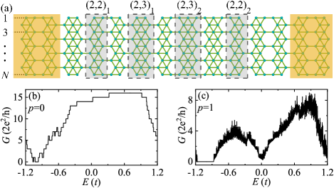
.–Borophene, a monolayer of boron atoms, has attracted extensive attention as a prototype for exploring novel two-dimensional (2D) systems zzes ; ajm2 ; ld1 since its successful synthesis by two independent groups ajm ; bfj following theoretical predictions th1 ; lkc1 ; yx1 ; th2 ; th3 ; pes1 ; wx1 . In contrast to other 2D materials ssd ; mp1 ; bls , multiple borophene polymorphs including freestanding ones have been realized experimentally qzhong ; wli ; rwu ; bki ; nav ; pran ; fb1 , which exhibit in-plane anisotropy and are tunable by ambient growth conditions. Of particular interest are the planar and boron sheets, which consist of (2,2) and (2,3) chains, respectively. Here, the indices and of (,) represent, respectively, the number of atoms in the narrow and wide rows of a single boron chain qzh , as illustrated in Fig. 1(a). These two sheets possess many intriguing attributes, such as excellent mechanical strength and flexibility zz1 ; zzh , conventional superconductivity pes2 ; mga ; zy1 , Dirac fermions bfo ; mez ; bfjs , and ultrahigh thermal conductance ld1 ; zh1 .
On the other hand, line defects (LDs) exist in diverse 2D materials jla ; vdz ; ns1 ; co1 ; lm1 ; pr1 and strongly affect their electronic, magnetic, optical, mechanical, and thermal properties dgu ; lkou ; jts ; hhu ; khp1 ; jbd ; lx1 ; kt1 ; mvk ; hk1 ; wf1 . Very recently, a specific LD at the interface between (2,2) and (2,3) chains has been widely reported in experiments xli ; lx2 ; ywa ; ljk ; lli ; qli ; xli2 , owing to higher structural stability of borophene in the presence of LDs ywa ; sgx2 . Specifically, several distinct phases are synthesized from periodic self-assembly of LDs xli ; lx2 ; ywa , implying that (2,2) and (2,3) chains function as building blocks to construct novel boron sheets. These LDs could considerably modulate the electronic properties of borophene xli ; ljk ; jze and improve its mechanical response sgx2 , thus playing an important role in the discovery of exotic quantum phenomena and in device applications. Notice that the LDs in realistic borophene lack long-range order and structural disorder emerges simultaneously xli ; ywa . Until now, the LD-induced structural disorder has not yet been discussed and understanding this disorder may facilitate the elucidation of structure-property relationships.
In this Letter, we study theoretically the electron transport through two-terminal borophene nanoribbons (BNRs) with random distribution of LDs by connecting to left and right semi-infinite BNRs. These BNRs, termed as disordered BNRs, are assembled from random arrangement of (2,2) and (2,3) chains in the central scattering region (CSR) and leads to LD-induced structural disorder, as shown in Fig. 1(a). We find that both and BNRs exhibit metallic behavior, consistent with experiments pran ; fb1 ; qzh ; xli . Remarkably, although the overall electron transport efficiency is dramatically declined in the presence of LDs, some resonant peaks of conductance quantum appear in the transmission spectra of various disordered BNRs, regardless of nanoribbon length and LD distribution. By changing nanoribbon width, the disordered BNRs could present metal-insulator transition with tunable transmission gap in the insulating regime. Furthermore, two evolution phenomena of resonant peaks are revealed for disordered BNRs with different widths, showing that (i) all of the resonant peaks for odd width overlap perfectly with all those of two narrow BNRs and (ii) a specific resonant peak for width reappears at various BNRs with width and an integer.
Model.–Electron transport through two-terminal disordered BNRs is simulated by the Hamiltonian bfo ; mez : . Here, () creates (annihilates) an electron at site , is the potential energy, and is the nearest-neighbor hopping integral. According to the Landauer-Büttiker formula, the conductance is expressed as . The conductance quantum , the Green’s function , and the linewidth function , with the electron energy, the CSR Hamiltonian, and the retarded self-energy due to the coupling to the left/right semi-infinite BNR mpl1 ; mpl2 .
In the numerical calculations, the parameters are fixed to , (energy unit), and the length counted by all of the chains in the CSR is taken as , unless stated otherwise. We consider the most disordered BNRs with half of the chains being (2,3) ones () and the results are averaged over 2500 disordered samples.
Pure BNRs.–We first study the electron transport through pure BNRs with the CSR being a or BNR, as shown in Figs. 1(b) and 1(c). It clearly appears that both and BNRs exhibit metallic behavior which is consistent with experiments pran ; fb1 ; qzh ; xli , and their conductances are asymmetric about the line of owing to the electron-hole symmetry breaking. For the BNR, its transmission spectrum is characterized by many conductance plateaus quantized at integer multiples of as expected [Fig. 1(b)], because of the translational symmetry. By contrast, when the BNR is replaced by a one, the conductance declines and presents dramatic oscillating behavior instead of quantized plateaus [Fig. 1(c)], in accordance with first-principles calculations jze , because of LD-induced scattering at the CSR-lead interfaces.
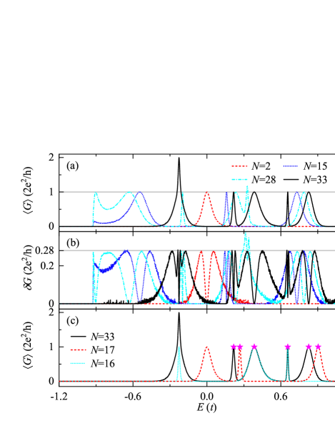
Disordered BNRs.–Figures 2(a) and 2(b) show energy-dependent averaged conductance and standard deviation , respectively, for disordered BNRs with different widths . Here, . One can see that the electron transport through disordered BNRs is strongly suppressed as expected, due to Anderson localization caused by successive scattering from randomly distributed LDs sm . However, it is surprising that some transmission peaks of are found in all these disordered BNRs and the peak number usually increases with [Figs. 2(a) and 4(b)]. In particular, the standard deviation at peak positions satisfies note1 and these peaks are robust against and sm , implying that the transmission peaks could be observed in any disordered BNR with arbitrary arrangement of LDs. This result explains a recent experiment that delocalized states are measured in BNRs with LDs ljk . These transmission peaks originate from resonant tunneling sm , where some resonant energies remain unchanged for BNRs with different and the others change with . Therefore, the electrons with invariant resonant energies cannot be reflected by LDs, as further demonstrated from spatial distributions of bond currents sm , leading to resonant peaks in disordered BNRs.
Besides, one can identify other important features. (i) The transport property of disordered BNRs strongly depends on , ranging from metallic [see the red-dashed line in Fig. 2(a)] to insulating behavior [see the other lines in Fig. 2(a)]. This indicates the width-driven metal-insulator transition in disordered BNRs. And the transmission gap is tunable in the insulating regime by varying , which is similar to graphene nanoribbons em ; syw ; hmy and facilitates band-gap engineering of BNRs. (ii) The resonant peaks, characterized by full width at half maximum (FWHM), are mainly categorized into narrow and wide peaks separated by about FWHM [Figs. 2(a) and 4(b)]. (iii) Each resonant conductance peak corresponds to two peaks in the curve of - [Fig. 2(b)]. Remarkably, the maximum of all these peaks satisfies which is close to reported in disordered graphene nanoribbons ada ; jcce . (iv) Some transmission peaks can even achieve [see the black-solid line in Fig. 2(a)], because of almost perfect superposition of two neighboring resonant peaks, as seen from the four-peak structure around in Fig. 2(b).
Evolution phenomenon (EP) I.–We then focus on the evolution of resonant peaks in disordered BNRs with various . Figure 2(c) shows vs for disordered BNRs with three . It clearly appears that some resonant peaks for are superimposed on all those for , while the remaining ones will overlap with all those for by properly moving peak positions. This phenomenon can also be observed in other disordered BNRs with, e.g., , , , and sm . Therefore, we conclude that all of the resonant peaks of disordered BNRs with odd width could be assembled from the ones with and , namely, EP I.
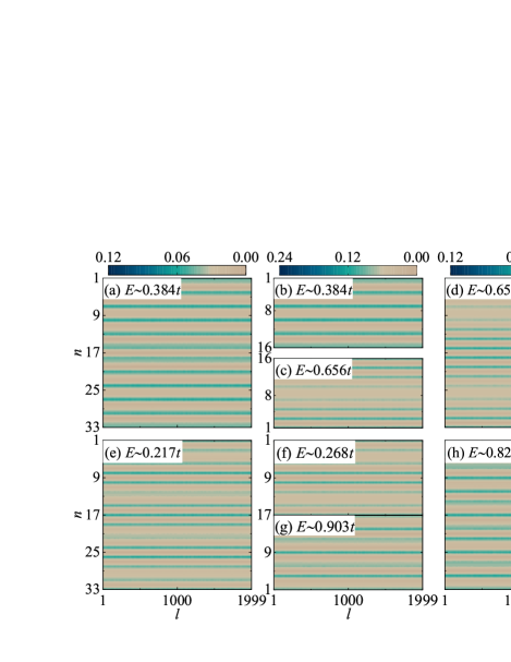
To elucidate the underlying physics of EP I, Fig. 3 plots spatial distributions of averaged interchain currents at typical resonant energies shown in Fig. 2(c). The currents flowing from the th chain to the th one read pjh ; acre ; chle : , where is the interchain lesser Green’s function. It is clear that all of the exhibit rather uniform fringe patterns and are independent of albeit the existence of randomly distributed LDs, manifesting delocalized states in various disordered BNRs. And green fringes denote transmission channels with finite , whose number and location depend on .
Since the spatial inversion symmetry with respect to the row of is preserved for disordered BNRs with odd [Fig. 1(a)], the corresponding possess mirror symmetry [Figs. 3(a) and 3(d)-3(h)] and can be divided into two cases according to the parity of wave functions. (i) The at are zero for [Figs. 3(a) and 3(d)], corresponding to odd wave functions whose electron densities are zero along the symmetric row of . In this situation, the top segment from to 16 and the bottom one from to 33, separated by this symmetric row, are independent of each other. Consequently, the transmission channels of the top/bottom segment for are the same as those for [Figs. 3(a) and 3(b); Figs. 3(c) and 3(d)], giving rise to completely identical resonant peaks at the same of these disordered BNRs. (ii) Contrarily, the are finite at [Figs. 3(e) and 3(h)], which refers to even wave functions with nonzero electron densities along the symmetric row. Interestingly, the transmission channels of the top/bottom segment for are also identical to those for albeit distinct magnitude of at the th row [Figs. 3(e) and 3(f); Figs. 3(g) and 3(h)]. Correspondingly, the disordered BNRs with and 33 possess identical resonant peaks but at different resonant energies, owing to the interference effect at the symmetric row. By contrast, the spatial inversion symmetry is destroyed for disordered BNRs with even and the parity of wave functions disappears simultaneously, leading to the absence of EP I for even .
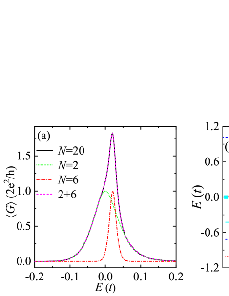
EP II.–Figure 4(a) shows vs around a transmission peak for three disordered BNRs, where the magenta-dashed line represents the sum of for and 6. One can see that the peak at for overlaps perfectly with the superposition of two neighboring peaks for and 6, as seen from the black-solid and magenta-dashed lines in Fig. 4(a). This indicates that a transmission peak of wide disordered BNRs could be evolved from narrow ones.
To further elucidate the above phenomenon, Fig. 4(b) displays a 2D plot of FWHM for all of the peaks as functions of and . It is clear that the number of squares increases with and some disordered BNRs possess peculiar resonant peaks with FWHM exceeding [see the leftmost peak for in Fig. 2(a) and the black squares in Fig. 4(b)]. In particular, completely identical resonant peaks are observed at for , 5, 8, …, at for , 9, 14, …, and at for , 13, … [see the cyan-solid, blue-dashed, and red-dotted lines in Fig. 4(b)]. Therefore, we infer that a resonant peak, firstly emerged in a disordered BNR with , will reappear at the same of various BNRs with , where is an integer and the period. This characteristic is named as EP II, which compensates EP I. Notice that the peak at for deviates from EP II [see the surrounded blue square in Fig. 4(b)], because of finite-size effects. By increasing , this transmission peak is split into two peaks at and [Fig. 4(a)]. Consequently, this surrounded square will be evolved into a cyan (red) square on the cyan-solid (red-dashed) line and EP II holds.
To gain insights into EP II, we consider a disordered BNR with . According to its unique structure, this disordered sample could be divided into basic BNRs with width , where the th BNR includes the rows from to and is separated from the th one by the th row, with and . For instance, the BNR with can be divided into two basic BNRs with , which are separated by the fifth row [Fig. 1(a)]. The Hamiltonian of this disordered BNR with width can then be partitioned as:
| (1) |
where and are the sub-Hamiltonians of the th basic BNR and the th row, respectively, and the hopping matrix from the th row to the th BNR when and from the th BNR to the th row when . Since the th and th BNRs are mirror images about the th row, the eigenstates of and are the same with identical eigenenergies, and the hopping matrices satisfy . Assuming the resonant state of the th basic BNR is described by the Schrödinger equation of , with the wave function and the resonant energy, the wave function of can then be constructed as:
| (2) |
Substituting Eqs. (1) and (2) into the Schrödinger equation, one obtains straightforwardly. Thus, disordered BNRs with possess a completely identical resonant peak for different . These results are further confirmed by the numerical results of bond currents sm .
.–In summary, the electron transport along disordered BNRs with random distribution of LDs is investigated. Our results indicate that although the overall electron transport efficiency is strongly declined, some resonant peaks are observed in the transmission spectra and leads to delocalized states in various disordered BNRs. These disordered BNRs could exhibit metal-insulator transition by varying nanoribbon width with tunable transmission gap in the insulating regime. Besides, the evolution of resonant peaks in disordered BNRs with different widths is explored, which is related to the spatial inversion symmetry.
Pei-Jia Hu thanks Jing-Ting Ding for useful discussions. This work is supported by the National Natural Science Foundation of China (Grants No. 11874428, No. 11874187, and No. 11921005), the National Key Research and Development Program of China (Grant No. 2017YFA0303301), and the High Performance Computing Center of Central South University.
References
- (1) Z. Zhang, E. S. Penev, and B. I. Yakobson, Two-dimensional boron: structures, properties and applications, Chem. Soc. Rev. 46, 6746 (2017).
- (2) A. J. Mannix, Z. Zhang, N. P. Guisinger, B. I. Yakobson and M. C. Hersam, Borophene as a prototype for synthetic 2D materials development, Nat. Nanotechnol. 13, 444 (2018).
- (3) D. Li, J. Gao, P. Cheng, J. He, Y. Yin, Y. Hu, L. Chen, Y. Cheng, and J. Zhao, 2D Boron Sheets: Structure, Growth, and Electronic and Thermal Transport Properties, Adv. Funct. Mater. 30, 1904349 (2020).
- (4) A. J. Mannix, X.-F. Zhou, B. Kiraly, J. D. Wood, D. Alducin, B. D. Myers, X. Liu, B. L. Fisher, U. Santiago, J. R. Guest, M. J. Yacaman, A. Ponce, A. R. Oganov, M. C. Hersam, and N. P. Guisinger, Synthesis of borophenes: Anisotropic, two-dimensional boron polymorphs, Science 350, 1513 (2015).
- (5) B. Feng, J. Zhang, Q. Zhong, W. Li, S. Li, H. Li, P. Cheng, S. Meng, L. Chen, and K. Wu, Experimental realization of two-dimensional boron sheets, Nat. Chem. 8, 563 (2016).
- (6) H. Tang and S. Ismail-Beigi, Novel Precursors for Boron Nanotubes: The Competition of Two-Center and Three-Center Bonding in Boron Sheets, Phys. Rev. Lett. 99, 115501 (2007).
- (7) K. C. Lau and R. Pandey, Stability and Electronic Properties of Atomistically-Engineered 2D Boron Sheets, J. Phys. Chem. C 111, 2906 (2007).
- (8) X. Yang, Y. Ding, and J. Ni, Ab initio prediction of stable boron sheets and boron nanotubes: Structure, stability, and electronic properties, Phys. Rev. B 77, 041402(R) (2008).
- (9) H. Tang and S. Ismail-Beigi, Self-doping in boron sheets from first principles: A route to structural design of metal boride nanostructures, Phys. Rev. B 80, 134113 (2009).
- (10) H. Tang and S. Ismail-Beigi, First-principles study of boron sheets and nanotubes, Phys. Rev. B 82, 115412 (2010).
- (11) E. S. Penev, S. Bhowmick, A. Sadrzadeh, and B. I. Yakobson, Polymorphism of Two-Dimensional Boron, Nano Lett. 12, 2441 (2012).
- (12) X. Wu, J. Dai, Y. Zhao, Z. Zhuo, J. Yang, and X. C. Zeng, Two-Dimensional Boron Monolayer Sheets, ACS Nano 6, 7443 (2012).
- (13) S. Das Sarma, S. Adam, E. H. Hwang, and E. Rossi, Electronic transport in two-dimensional graphene, Rev. Mod. Phys. 83, 407 (2011).
- (14) P. Miró, M. Audiffred, and T. Heine, An atlas of two-dimensional materials, Chem. Soc. Rev. 43, 6537 (2014).
- (15) S. Barraza-Lopez, B. M. Fregoso, J. W. Villanova, S. S. P. Parkin, and K. Chang, Colloquium: Physical properties of group-IV monochalcogenide monolayers, Rev. Mod. Phys. 93, 011001 (2021).
- (16) Q. Zhong, J. Zhang, P. Cheng, B. Feng, W. Li, S. Sheng, H. Li, S. Meng, L. Chen, and K. Wu, Metastable phases of 2D boron sheets on Ag(111), J. Phys.: Condens. Matter 29, 095002 (2017).
- (17) W. Li, L. Kong, C. Chen, J. Gou, S. Sheng, W. Zhang, H. Li, L. Chen, P. Cheng, and K. Wu, Experimental realization of honeycomb borophene, Sci. Bull. 63, 282 (2018).
- (18) R. Wu, I. K. Drozdov, S. Eltinge, P. Zahl, S. Ismail-Beigi, I. Boović, and A. Gozar, Large-area single-crystal sheets of borophene on Cu(111) surfaces, Nat. Nanotechnol. 14, 44 (2019).
- (19) B. Kiraly, X. Liu, L. Wang, Z. Zhang, A. J. Mannix, B. L. Fisher, B. I. Yakobson, M. C. Hersam, and N. P. Guisinger, Borophene Synthesis on Au(111), ACS Nano 13, 3816 (2019).
- (20) N. A. Vinogradov, A. Lyalin, T. Taketsugu, A. S. Vinogradov, and A. Preobrajenski, Single-Phase Borophene on Ir(111): Formation, Structure, and Decoupling from the Support, ACS Nano 13, 14511 (2019).
- (21) P. Ranjan, T. K. Sahu, R. Bhushan, S. S. Yamijala, D. J. Late, P. Kumar, and A. Vinu, Freestanding Borophene and Its Hybrids, Adv. Mater. 31, 1900353 (2019).
- (22) B. Feng, J. Zhang, R.-Y. Liu, T. Iimori, C. Lian, H. Li, L. Chen, K. Wu, S. Meng, F. Komori, and I. Matsuda, Direct evidence of metallic bands in a monolayer boron sheet, Phys. Rev. B 94, 041408(R) (2016).
- (23) Q. Zhong, L. Kong, J. Gou, W. Li, S. Sheng, S. Yang, P. Cheng, H. Li, K. Wu, and L. Chen, Synthesis of borophene nanoribbons on Ag(110) surface, Phys. Rev. Mater. 1, 021001(R) (2017).
- (24) Z. Zhang, A. J. Mannix, Z. Hu, B. Kiraly, N. P. Guisinger, M. C. Hersam, and B. I. Yakobson, Substrate-Induced Nanoscale Undulations of Borophene on Silver, Nano Lett. 16, 6622 (2016).
- (25) Z. Zhang, Y. Yang, E. S. Penev, and B. I. Yakobson, Elasticity, Flexibility, and Ideal Strength of Borophenes, Adv. Funct. Mater. 27, 1605059 (2017).
- (26) E. S. Penev, A. Kutana, and B. I. Yakobson, Can Two-Dimensional Boron Superconduct? Nano Lett. 16, 2522 (2016).
- (27) M. Gao, Q.-Z. Li, X.-W. Yan, and J. Wang, Prediction of phonon-mediated superconductivity in borophene, Phys. Rev. B 95, 024505 (2017).
- (28) Y. Zhao, S. Zeng, C. Lian, Z. Dai, S. Meng, and J. Ni, Multigap anisotropic superconductivity in borophenes, Phys. Rev. B 98, 134514 (2018).
- (29) B. Feng, O. Sugino, R.-Y. Liu, J. Zhang, R. Yukawa, M. Kawamura, T. Iimori, H. Kim, Y. Hasegawa, H. Li, L. Chen, K. Wu, H. Kumigashira, F. Komori, T.-C. Chiang, S. Meng, and I. Matsuda, Dirac Fermions in Borophene, Phys. Rev. Lett. 118, 096401 (2017).
- (30) M. Ezawa, Triplet fermions and Dirac fermions in borophene, Phys. Rev. B 96, 035425 (2017).
- (31) B. Feng, J. Zhang, S. Ito, M. Arita, C. Cheng, L. Chen, K. Wu, F. Komori, O. Sugino, K. Miyamoto, T. Okuda, S. Meng, and I. Matsuda, Discovery of 2D Anisotropic Dirac Cones, Adv. Mater. 30, 1704025 (2018).
- (32) H. Zhou, Y. Cai, G. Zhang, and Y.-W. Zhang, Superior lattice thermal conductance of single-layer borophene, npj 2D Mater. Appl. 1, 14 (2017).
- (33) J. Lahiri, Y. Lin, P. Bozkurt, I. I. Oleynik, and M. Batzill, An extended defect in graphene as a metallic wire, Nat. Nanotechnol. 5, 326 (2010).
- (34) A. M. van der Zande, P. Y. Huang, D. A. Chenet, T. C. Berkelbach, Y. You, G.-H. Lee, T. F. Heinz, D. R. Reichman, D. A. Muller, and J. C. Hone, Grains and grain boundaries in highly crystalline monolayer molybdenum disulphide, Nat. Mater. 12, 554 (2013).
- (35) S. Najmaei, Z. Liu, W. Zhou, X. Zou, G. Shi, S. Lei, B. I. Yakobson, J.-C. Idrobo, P. M. Ajayan, and J. Lou, Vapour phase growth and grain boundary structure of molybdenum disulphide atomic layers, Nat. Mater. 12, 754 (2013).
- (36) O. Cretu, Y.-C. Lin, and K. Suenaga, Evidence for Active Atomic Defects in Monolayer Hexagonal Boron Nitride: A New Mechanism of Plasticity in Two-Dimensional Materials, Nano Lett. 14, 1064 (2014).
- (37) M. Liu, M. Liu, L. She, Z. Zha, J. Pan, S. Li, T. Li, Y. He, Z. Cai, J. Wang, Y. Zheng, X. Qiu, and D. Zhong, Graphene-like nanoribbons periodically embedded with four- and eight-membered rings, Nat. Commun. 8, 14924 (2017).
- (38) R. Pawlak, C. Drechsel, P. D’Astolfo, M. Kisiel, E. Meyer, and J. I. Cerda, Quantitative determination of atomic buckling of silicene by atomic force microscopy, Proc. Natl. Acad. Sci. U.S.A. 117, 228 (2020).
- (39) D. Gunlycke and C. T. White, Graphene Valley Filter Using a Line Defect, Phys. Rev. Lett. 106, 136806 (2011).
- (40) L. Kou, C. Tang, W. Guo, and C. Chen, Tunable Magnetism in Strained Graphene with Topological Line Defect, ACS Nano 5, 1012 (2011).
- (41) J. Song, H. Liu, H. Jiang, Q.-f. Sun, and X. C. Xie, One-dimensional quantum channel in a graphene line defect, Phys. Rev. B 86, 085437 (2012).
- (42) H. Huang, Y. Xu, X. Zou, J. Wu, and W. Duan, Tuning thermal conduction via extended defects in graphene, Phys. Rev. B 87, 205415 (2013).
- (43) H.-P. Komsa, S. Kurasch, O. Lehtinen, U. Kaiser, and A. V. Krasheninnikov, From point to extended defects in two-dimensional MoS2: Evolution of atomic structure under electron irradiation, Phys. Rev. B 88, 035301 (2013).
- (44) J. B. de Oliveira, I. S. S. de Oliveira, J. E. Padilha, and R. H. Miwa, Tunable magnetism and spin-polarized electronic transport in graphene mediated by molecular functionalization of extended defects, Phys. Rev. B 97, 045107 (2018).
- (45) X. Li, S. Zhang, H. Huang, L. Hu, F. Liu, and Q. Wang, Unidirectional Spin-Orbit Interaction Induced by the Line Defect in Monolayer Transition Metal Dichalcogenides for High-Performance Devices, Nano Lett. 19, 6005 (2019).
- (46) T. Kähärä and P. Koskinen, Rippling of two-dimensional materials by line defects, Phys. Rev. B 102, 075433 (2020).
- (47) M. V. Kondrin, Y. B. Lebed, and V. V. Brazhkin, Extended Defects in Graphene and Their Contribution to the Excess Specific Heat at High Temperatures, Phys. Rev. Lett. 126, 165501 (2021).
- (48) K. Hsieh, V. Kochat, T. Biswas, C. S. Tiwary, A. Mishra, G. Ramalingam, A. Jayaraman, K. Chattopadhyay, S. Raghavan, M. Jain, and A. Ghosh, Spontaneous Time-Reversal Symmetry Breaking at Individual Grain Boundaries in Graphene, Phys. Rev. Lett. 126, 206803 (2021).
- (49) F. Wan, X. Wang, Y. Guo, J. Zhang, Z. Wen, and Y. Li, Role of line defect in the bandgap and transport properties of silicene nanoribbons, Phys. Rev. B 104, 195413 (2021).
- (50) X. Liu, Z. Zhang, L. Wang, B. I. Yakobson, and M. C. Hersam, Intermixing and periodic self-assembly of borophene line defects, Nat. Mater. 17, 783 (2018).
- (51) X. Liu, L. Wang, S. Li, M. S. Rahn, B. I. Yakobson, and M. C. Hersam, Geometric imaging of borophene polymorphs with functionalized probes, Nat. Commun. 10, 1642 (2019).
- (52) Y. Wang, L. Kong, C. Chen, P. Cheng, B. Feng, K. Wu, and L. Chen, Realization of Regular-Mixed Quasi-1D Borophene Chains with Long-Range Order, Adv. Mater. 32, 2005128 (2020).
- (53) L. Kong, L. Liu, L. Chen, Q. Zhong, P. Cheng, H. Li, Z. Zhang and K. Wu, One-dimensional nearly free electron states in borophene, Nanoscale 11, 15605 (2019).
- (54) L. Liu, Z. Zhang, X. Liu, X. Xuan, B. I. Yakobson, M. C. Hersam, and W. Guo, Borophene Concentric Superlattices via Self-Assembly of Twin Boundaries, Nano Lett. 20, 1315 (2020).
- (55) Q. Li, V. S. C. Kolluru, M. S. Rahn, E. Schwenker, S. Li, R. G. Hennig, P. Darancet, M. K. Y. Chan, and M. C. Hersam, Synthesis of borophane polymorphs through hydrogenation of borophene, Science 371, 1143 (2021).
- (56) X. Liu, L. Wang, B. I. Yakobson, and M. C. Hersam, Nanoscale Probing of Image-Potential States and Electron Transfer Doping in Borophene Polymorphs, Nano Lett. 21, 1169 (2021).
- (57) S.-G. Xu, C.-C. He, Y.-J. Zhao, H. Xu, and X.-B. Yang, Unconventional line defects engineering in two-dimensional boron monolayers, Phys. Rev. Mater. 5, 044003 (2021).
- (58) J. Zeng and K.-Q. Chen, Charge Transport in Borophene: Role of Intrinsic Line Defects, J. Phys. Chem. C 123, 6270 (2019).
- (59) M. P. Lopez Sancho, J. M. Lopez Sancho, and J. Rubio, Quick iterative scheme for the calculation of transfer matrices: Application to Mo(100), J. Phys. F: Met. Phys. 14, 1205 (1984).
- (60) M. P. Lopez Sancho, J. M. Lopez Sancho, and J. Rubio, Highly convergent schemes for the calculation of bulk and surface Green functions, J. Phys. F: Met. Phys. 15, 851 (1985).
- (61) See Supplemental Material for (i) robustness of transmission peaks against LDs, (ii) physical origin of transmission peaks in disordered BNRs, and (iii) more details of evolution phenomena I and II.
- (62) The standard deviation is nonzero at the resonant energies (i.e., peak positions) of for and of and for , because the conductance contributed only from neighboring resonant peak(s) at these energies fluctuates due to finite-size effects-induced long tails of transmission peaks. We emphasize that at these resonant energies for longer disordered BNRs.
- (63) M. Ezawa, Peculiar width dependence of the electronic properties of carbon nanoribbons, Phys. Rev. B 73, 045432 (2006).
- (64) Y.-W. Son, M. L. Cohen, and S. G. Louie, Energy Gaps in Graphene Nanoribbons, Phys. Rev. Lett. 97, 216803 (2006).
- (65) M. Y. Han, B. Özyilmaz, Y. Zhang, and P. Kim, Energy Band-Gap Engineering of Graphene Nanoribbons, Phys. Rev. Lett. 98, 206805 (2007).
- (66) D. A. Abanin and L. S. Levitov, Quantized Transport in Graphene p-n Junctions in a Magnetic Field, Science 317, 641 (2007).
- (67) J.-C. Chen, H. Zhang, S.-Q. Shen, and Q.-F. Sun, Dephasing effect on transport of a graphene p-n junction in a quantum Hall regime, J. Phys.: Condens. Matter 23, 495301 (2011).
- (68) P.-J. Hu, S.-X. Wang, X.-H. Gao, Y.-Y. Zhang, T.-F. Fang, A.-M. Guo, and Q.-F. Sun, Spin-dependent electron transport along hairpinlike DNA molecules, Phys. Rev. B 102, 195406 (2020).
- (69) A. Cresti, R. Farchioni, G. Grosso, and G. P. Parravicini, Keldysh-Green function formalism for current profiles in mesoscopic systems, Phys. Rev. B 68, 075306 (2003).
- (70) C. H. Lewenkopf and E. R. Mucciolo, The recursive Green’s function method for graphene, J. Comput. Electron. 12, 203 (2013).