Metallization and proximity superconductivity in topological insulator nanowires
Abstract
A heterostructure consisting of a topological insulator (TI) nanowire brought into proximity with a superconducting layer provides a promising route to achieve topological superconductivity and associated Majorana bound states (MBSs). Here, we study effects caused by such a coupling between a thin layer of an -wave superconductor and a TI nanowire. We show that there is a distinct phenomenology arising from the metallization of states in the TI nanowire by the superconductor. In the strong coupling limit, required to induce a large superconducting pairing potential, we find that metallization results in a shift of the TI nanowire subbands ( meV) as well as it leads to a small reduction in the size of the subband gap opened by a magnetic field applied parallel to the nanowire axis. Surprisingly, we find that metallization effects in TI nanowires can also be beneficial. Most notably, coupling to the superconductor induces a potential in the portion of the TI nanowire close to the interface with the superconductor, this breaks inversion symmetry and at finite momentum lifts the spin degeneracy of states within a subband. As such coupling to a superconductor can create or enhance the subband splitting that is key to achieving topological superconductivity. This is in stark contrast to semiconductors, where it has been shown that metallization effects always reduce the equivalent subband-splitting caused by spin-orbit coupling. We also find that in certain geometries metallization effects can reduce the critical magnetic required to enter the topological phase. We conclude that, unlike in semiconductors, the metallization effects that occur in TI nanowires can be relatively easily mitigated, for instance by modifying the geometry of the attached superconductor or by compensation of the TI material.
I Introduction
Topological superconductors can host localized excitations known as Majorana fermions, for instance at their boundaries or within vortices [1, 2]. It has been argued that the non-Abelian statistics and localized nature of Majorana fermions make them promising candidates for quantum computation [3, 4, 5]. One route to achieve topological superconductivity is via the proximity effect in which a trivial -wave superconductor induces a pairing potential in another material. For instance, due to the proximity effect a superconductor coupled to the surface of a topological insulator (TI) can give rise to a superconductivity where Majorana bound states (MBSs) are predicted to appear at the center of vortices [6, 7, 8].
Another proposed platform to achieve MBSs is a thin nanowire of three-dimensional topological insulators with quantum confined surface states [9]. When brought into proximity with a superconductor, as it has been shown theoretically, a topological phase of large extend in the parameter space can be achieved in a TI nanowire, either when the superconducting order parameter possesses a vortex [10] – essentially requiring a full superconducting shell [11] – or without a vortex [12] – requiring the breaking of inversion symmetry by, for example, the application of a gate. Since a full superconducting shell is not experimentally feasible in the near term, we will focus on setups without a vortex in the order parameter.
In the past few years there has been substantial progress in the growth of thin TI nanowire devices [9, 13, 14, 15, 16, 17, 18, 19, 20, 21], including the growth of bulk insulating devices in which the chemical potential can be tuned close to the Dirac point [22, 23]. In TI nanowires several transport signatures of the quantum confinement of surface states have been reported, previously these consisted of conductivity oscillations [24, 25] as a function of magnetic field or gate voltage [13, 14, 15, 16, 17, 18, 19, 20, 21, 22]. Recently, a non-reciprocal transport effect in bulk insulating nanowires provided strong evidence not only for quantum confinement of the surface states but also for the splitting of initially spin-degenerate subbands that is predicted due to the breaking of inversion symmetry by a non-uniform potential through the cross-section of the nanowire [23]. This subband-splitting is a key element required to achieve MBSs without a vortex [12].
Given the substantial recent progress in TI nanowire fabrication, the experimental focus now turns to devices where superconductivity is induced in the TI nanowire via the proximity effect [9, 26, 27, 28, 29, 30, 31, 32, 33]. Such a device is shown in Fig. 1 where the TI nanowire is strongly tunnel coupled to a thin layer ( nm) of superconductor. In semiconductors that possess strong Rashba spin-orbit coupling – which have also been predicted to host MBSs in certain circumstances [34, 35] – the full influence of the tunnel coupling to a superconducting layer has previously been analysed [36, 37, 38, 39, 40, 41] and revealed a significant roadblock to achieving MBSs in semiconductors is the metallization of the semiconductor by the superconductor. Metallization [37, 38] is the process by which, when a large pairing potential is induced in the semiconductor, other properties of the semiconductor are renormalized towards the values of the attached superconducting metal. Namely, it was shown in Ref. 38 that inducing a pairing potential of the order found in the parent superconductor () – referred to as strong coupling – also results in a large subband-shift ( meV), a significant increase in the effective mass (), and a considerable reduction of the -factor and the spin-orbit energy. In other words, a large proximity induced gap also results in a considerable reduction of the material properties that made the semiconductor desirable for achieving MBSs in the first place.
In this paper we consider the impact of tunnel coupling a thin layer of superconductor to a TI nanowire. Since a TI is closer to a metallic state than a semiconductor and the two-dimensional cross-section of a TI nanowire is fundamental to its nature, we can expect a unique impact of the superconductor on the TI nanowire. Indeed, whilst we find that TI nanowires undergo some similar metallization effects to semiconductors in the strong coupling limit, the size of the metallization effects are smaller than in semiconductors, for instance we find a subband-shift meV and a small reduction in the gap induced by orbital effects from a magnetic field parallel to the TI nanowire. Unlike in semiconductors, we find that metallization effects in TI nanowires can actually be beneficial. For instance, in a semiconductor the spin-orbit energy is reduced by the coupling to a superconductor, however, in a TI nanowire the subband splitting energy can actually be created or enhanced in the strong coupling regime since the superconductor provides an inversion symmetry breaking potential similar to that produced by a gate. We also show that the superconducting gap is highly momentum dependent for certain device geometries such that the magnetic field strength required to reach the topological phase can be reduced due to metallization effects. Our findings show that, unlike in semiconductors, metallization effects in TI nanowires can relatively easily be mitigated and do not pose as significant a roadblock to achieving MBSs.
The paper is organized as follows. In Sec. II we discuss the main ingredients that are required to achieve topological superconductivity in TI nanowires, as outlined in Ref. 12. In Sec III we present the tight binding model that we use to investigate the coupling of a superconducting layer to a TI nanowire. Sec. IV investigates the impact metallization effects have on the features of a TI nanowire that are required to achieve MBSs. This is done first without and then including the effects of a non-uniform potential induced by a gate. Sec. V outlines how the metallization in TI nanowires can be experimentally mitigated and also compares these metallization effects to the equivalent effects that occur in semiconductor devices. Finally in Sec. VI we discuss the wider implications of our findings for the prospects of realizing MBSs in TI nanowire devices.
II Topological superconductivity
in TI nanowires
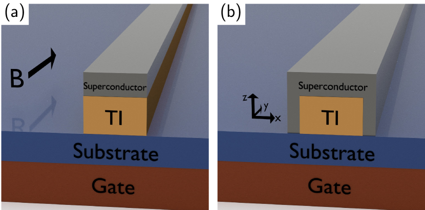
We begin by outlining the main ingredients that are required to achieve topological superconductivity and Majorana bound states in TI nanowires, further details can be found in Ref. 12. The heterostructure we consider is shown in Fig. 1. It consists of a TI nanowire (gold color) that is tunnel coupled to a superconductor (gray color), the chemical potential in the TI nanowire can be adjusted via a gate below the nanowire (red color). The superconductor can either be attached only to the top of the nanowire (Fig. 1a) or to multiple surfaces such as in a horseshoe arrangement (Fig. 1b). MBSs at the ends of the nanowire can be generated in this setup when a magnetic field applied parallel to the nanowire axis results in a topological superconducting phase (see Fig. 2).
We first consider the TI nanowire when there is no tunnel coupling to the superconductor. If, in addition, no gate voltage is applied, the spectrum of the TI nanowire is given by [10, 12]
| (1) |
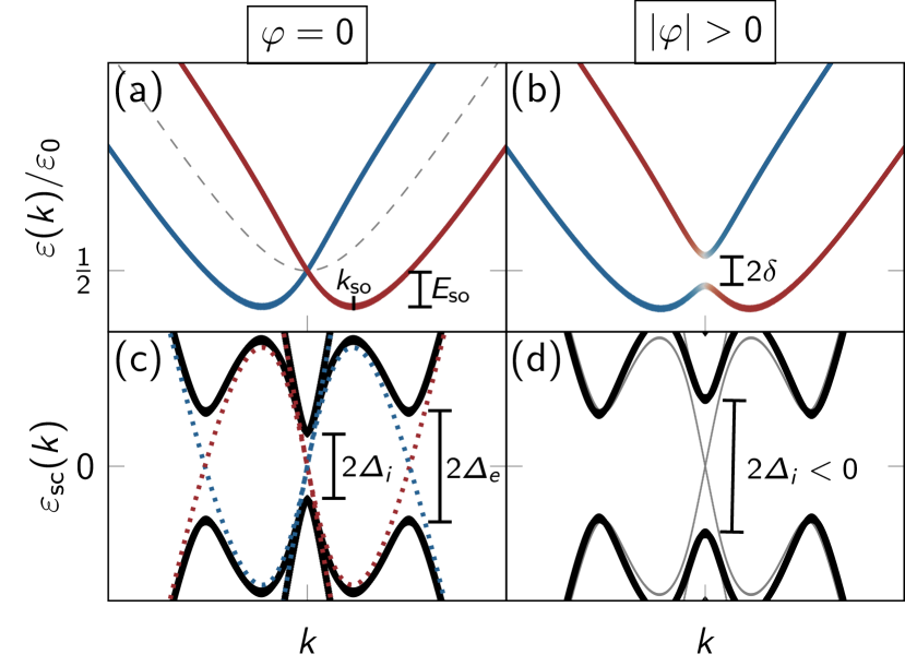
where , is the Fermi velocity, is the momentum along the wire, and and is the perimeter of the nanowire [see dashed gray line in Fig. 2(a)]. The spectrum of Eq. (1) describes doubly degenerate subbands which are equally spaced by as has been shown to hold for many different TI nanowire cross-sections [11]. For instance, the left panel of Fig. 3 shows the spectrum for a rectangular cross-section without coupling to the superconductor (see next section for details). Throughout this study we will consider a rectangular cross-section – such a cross-section is produced, for example, by etching MBE films [23]– although the metallization phenomena we find will be generally applicable to any nanowire cross-section.
Applying a gate voltage, one induces a spatially non-uniform potential in the nanowire cross-section [12], , where is the average of the potential and is the non-uniform component, with the polar angle within the nanowire cross-section. The non-uniform component arises because the gate is located only on one side of the nanowire. This non-uniform potential breaks inversion symmetry and lifts the degeneracy of the subbands at finite momentum along the nanowire [see Fig. 2(a)]. For a non-uniformity with components that are small compared to the subband spacing the spectrum becomes [12]
| (2) |
where we have used the original angular momenta to label the split subband pair. As such the presence of the non-uniform chemical potential results in a subband-splitting with an energy scale [see Fig. 2(a)]. Note that the non-uniform component of the chemical potential does not alter the energy of the states at and they are only shifted by the average of the gate induced potential , this effect is associated with Klein-tunnelling.
A magnetic field, , applied parallel to the nanowire – indicated by the black arrow in Fig. 1 – opens a gap of size at primarily due to orbital effects, where is the magnetic flux (here is the cross-sectional area of the nanowire) in units of the fundamental flux quantum . If the chemical potential lies within this magnetic field induced gap it leaves only a pair of (almost) helical modes [42, 43, 44] at finite Fermi momenta [see Fig. 2(b)].
When the TI nanowire is brought into proximity with an -wave superconductor, a pairing potential is induced in the TI. It should be noted that in general the induced pairing potential is momentum dependent (see Fig. 2). In particular, as a result of a non-uniform potential, the wavefunctions of states close to are more uniformly distributed around the nanowire perimeter than states at large momenta (see below). As a result of these differently localized wavefunctions we can identify two gaps in the spectrum of the resulting energy spectrum: An interior gap at and an exterior gap at large momenta (see Fig. 2c). If in addition to the proximity induced pairing, a magnetic field is applied along the nanowire, then a topological superconducting phase can be achieved when [12]
| (3) |
where is measured from the subband crossing point at . Within this topological phase MBSs appear at the ends of the TI nanowire, due to both the large subband-splitting energy and ease of opening a field induced gap the phase space for MBSs can be exceptionally large ( meV).
The key features of TI nanowires that enable a large topological superconducting phase are the large splitting energy due to a non-uniform potential meV and the field-induced large gap due to orbital effects meV/T (equivalent to a g-factor ). However, in the limit of strong coupling between TI and superconductor it can be expected that metallization effects on the TI nanowire due to the superconductor will modify these desirable properties. In the remainder of this manuscript we will investigate the impact of these metallization effects in the strong coupling regime and the challenge they pose to achieving a topological superconducting phase in the TI nanowire.
III Model
To model the superconducting proximity effect and metallization effects in the setup shown in Fig. 1, we use a tight binding model with translational invariance along the length of the system (-direction in Fig. 1) such that the momentum parallel to the nanowire remains a good quantum number [38]. The total Hamiltonian of the coupled superconductor and TI nanowire can therefore be written as , where for each we define
| (4) |
where is the Hamiltonian of the TI nanowire, is the Hamiltonian of the superconductor, and describes the tunnel coupling between TI nanowire and superconductor.
To model the TI we use the BHZ Hamiltonian [45, 46, 47] on a square lattice with a rectangular cross-section, such that
| (5) |
where . Here, is a 4-vector, where describes the creation of an electron (hole ) with spin on site in the cross-section and with momentum along the nanowire. The influence of a gate will be modelled by the local potential . Throughout we choose the lattice constant Å such that the rectangular cross-section is of width and height with and , which means that the nanowire cross-section is approximately of dimension . Orbital effects due to the magnetic field parallel to the nanowire, which open a gap at , are taken into account through the Peierls phases and . For clarity and simplicity we chose BHZ model parameters that are isotropic along all three axes, but such that they are consistent with Bi2Se3[47], namely meVÅ, meVÅ2, and meV. Note that the finite extent of the wavefunction into the bulk of the nanowire means that the effective perimeter of the TI nanowire spectrum, Eq. (1), is smaller than this. As such we define the subband spacing using the gap between the subbands closest to the charge neutrality point of the BHZ model (see left panel of Fig. 3).
The Hamiltonian of the superconductor is given by [38]
| (6) |
where and are the corresponding creation and annihilation operators for the electrons in the superconductor, respectively, the spin values of the electrons along the quantization axis, and where we choose the lattice constant of the superconductor, Å, to be the same as that used in the BHZ model for the TI (see above). We consider different shapes and heights of superconductors, therefore the sums run over all sites of the superconductor and indicates a sum over nearest neighbour sites. For numerical simplicity we do not model any specific superconductor, however, throughout we use parameters which give reasonable electronic properties compared to those found in, for example, niobium or vanadium. Namely, we choose the hopping eV and set the chemical potential in the superconductor to , this corresponds to an effective mass and Fermi velocity m/s.
Finally, the tunnelling between the TI and superconductor is described by hopping from sites on either side of the interface between the two subsystems, these sites are denoted by . The coupling Hamiltonian between TI and superconductor is therefore given by
| (7) | ||||
where denotes the particle/hole degree of freedom of the BHZ model. As such, the hopping between adjacent sites preserves spin but otherwise the coupling is isotropic between the degrees of freedom of the TI and those of the superconductor.
IV Metallization effects
To begin we consider a setup with the superconductor only on top of the TI nanowire as shown in Fig. 1(a). We will discuss the potential advantages of the horseshoe-shaped superconductor shown in Fig. 1(b) in the next section.
IV.1 Effect of tunnel coupling to superconductor
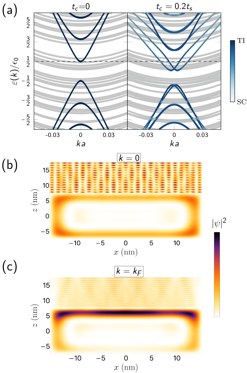
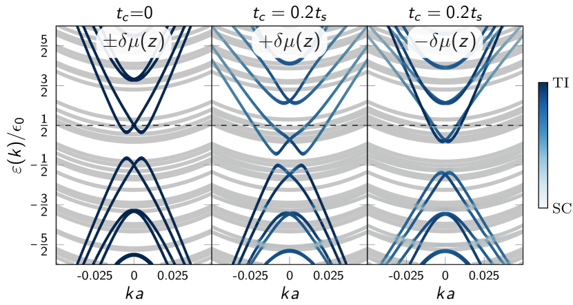
We first consider the impact of coupling the superconductor to the TI nanowire in the absence of non-uniform potential generated by an applied gate voltage. The TI nanowire energy spectrum for a finite coupling is shown in Fig. 3, the most notable features are a subband-shift similar in size to the subband spacing , a subband-splitting at finite momenta, and a renormalization of Fermi velocity.
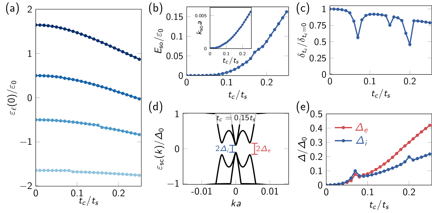
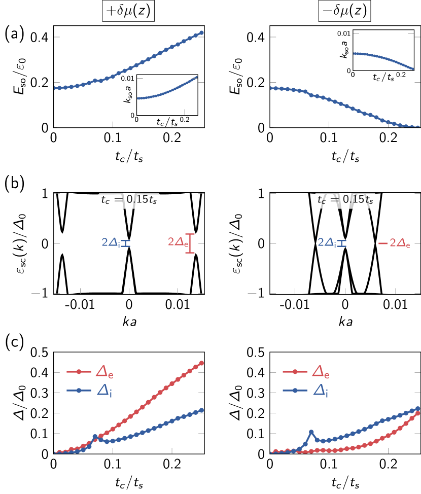
As shown in Fig. 3, there is subband-shift when the superconducting layer is coupled to the TI nanowire, similar to the subband-shift previously investigated in semiconductors. This subband-shift is most easily quantified by considering the change of the subband energy at zero momentum, . The full dependence of this shift in with respect to the tunnel coupling is shown in Fig. 4(a). We find that this shift reaches values of the order of the subband spacing meV for realistic parameters, which is smaller than the effect in semiconductors [38]. We also observe that the shift of the subbands is always -type and is strongly dependent on the subband index .
Possibly the most striking feature of Fig. 3 is the subband-splitting resulting from the coupling to the superconductor. As discussed in Sec. II, a non-uniform potential through the nanowire cross-section can induce such a subband-splitting. Above we considered a non-uniformity created due to gating, however, the potential resulting from a superconductor attached to only one side of the nanowire also results in a sizable non-uniform potential with the effect largest close to the interface. As a result, the coupling to a superconductor by itself results in a subband splitting of size . The evolution of the splitting-energy as a function of increasing coupling strength is shown in Fig. 4(b). Additionally, since for small momenta only the average of the potential induced by the superconductor, , results in a subband-shift, the large non-uniformity of the potential also partially explains why the overall subband-shift (discussed above) is smaller compared to that found in semiconductors.
The size of the field-induced gap at , , is also modified by the tunnel coupling to a superconductor. As shown in Fig. 4(c) it is renormalized down and substantial reductions occur when the crossing point at coincides with the bottom of subband of the superconductor [resulting in the dips shown in Fig. 4(c)]. We find that the size of the gap is directly proportional to the weight of the TI state in the superconductor.
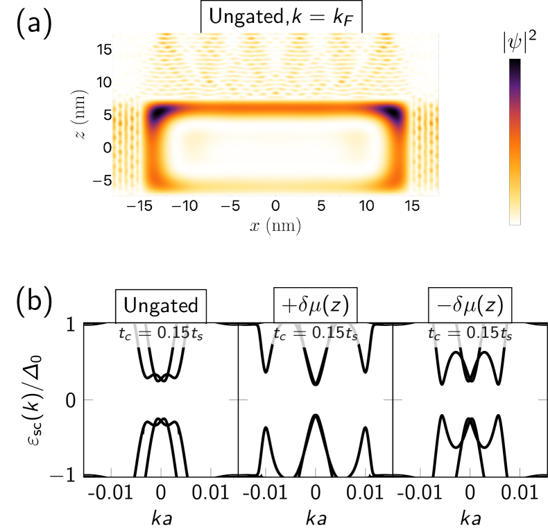
Moving now to the discussion of the size of the proximity-induced pairing potential in the TI nanowire, in Fig. 4(d), we analyze the typical spectra for the chemical potential tuned to the subband crossing point at . We see that the size of the resulting superconducting gap is -dependent leading to an interior gap close to to be of different size compared to the exterior gap . The reason for the momentum-dependent gap stems from the fact that finite momenta states are more localized at the top of the TI compared to the states near (see Fig. 4) and therefore states at large finite momenta couple more efficiently to the superconductor (note that if a gate voltage is applied the opposite effect can occur, see below). When the chemical potential is tuned close to the subband crossing point of the lowest subband, this momentum dependence can reduce the magnetic field strength required to achieve the topological superconducting phase, in accordance with the topological phase transition criterion defined in Eq. (3). This is a useful effect as it helps to reduce the detrimental impact of the magnetic field on the parent superconductor itself.
IV.2 Impact of gating
We now consider the interplay of gating and metallization effects. As discussed in the Sec. II, the application of a gate breaks inversion symmetry which lifts the degeneracy of subbands at finite momenta and results in a splitting of the subbands with individual states localized close to or far from the gate, depending on the sign of the applied gate voltage (see Fig. 5 far left panel).
As discussed above, the induced potential at the interface with the superconductor can result in a similar localization of the states on one surface of the TI nanowire and associated splitting of the TI nanowire subbands. To model this we use a potential which varies in the vertical (-direction) through the TI nanowire cross-section such that with measured from the center of the nanowire. It was previously shown that the induced subband splitting is not strongly dependent on the exact shape of the gate induced non-uniform potential (see Ref. [12]). We find that the interplay between the gate voltage and potential arising from the superconductor can either enhance or reduce the size of the subband splitting, , depending on the relative sign of the induced potentials from the gate and superconductor, see Fig. 5. If the sign of the non-uniform potential induced by the gate and by superconductor on the surface adjacent the superconductor are opposite the total subband-splitting is reduced, however, if the signs are the same the subband-splitting is enhanced. We note that this is in strong contrast with semiconductors, where the equivalent subband-splitting due to spin-orbit coupling is a materials property and is therefore reduced by metallization effects [38]. A plot of this splitting energy as a function of the tunnel coupling strength is shown in Fig. 6(a) for both signs of gate induced potential.
The impact the non-uniform potential, , arising due to gating, on the induced pairing potential, , is shown in Fig. 6(b). Here, the chemical potential is kept at the subband crossing point at of the lowest subband. Whilst the interior gap is similar in magnitude for both signs of gate potential, the exterior gap differs dramatically. Strikingly, a negligibly small exterior gap is present when the gate and superconductor-induced potentials compete [], whereas when the potentials complement each other [] the exterior gap is much larger than the interior gap in the strong coupling regime. Finally, in Fig. 6(c), we demonstrate the evolution of the interior and exterior gaps as a function of the tunnel coupling . When the gate-induced and superconductor-induced non-uniform potentials complement each other, the evolution of the induced gap is similar to that of the ungated nanowire [left panel of Fig. 6(c)], whilst when the potentials compete the exterior gap is negligible up to the tunnelling strengths at which [right panel Fig. 6(c)].
V Experimental considerations and comparison with semiconductors
V.1 Metallization effects
In the previous section we saw that a strong tunnel coupling between a superconducting layer and a TI nanowire leads to a shift and splitting of the TI nanowire subbands as well as a reduction of the size of the possible gap opened by orbital effects when a magnetic field is applied parallel to the nanowire. In this section we will consider the challenges posed by and possible mitigations of these effects possible in experiments. The main criteria for achieving MBSs in TI nanowires are: 1) A large exterior gap . 2) The ability to tune the chemical potential close to the subband crossing. 3) A large splitting energy such that helical modes cross the Fermi-level at large finite momentum. 4) A magnetic field induced gap which can exceed the size of the interior superconducting gap at field strengths lower than the critical field of the superconductor, such that the topological criterion in Eq. (3) can be satisfied.
We first note that our results show that, unlike in semiconductor nanowires, metallization effects in TI nanowires pose a more limited experimental challenge to the ability to fulfil the requirements for topological superconductivity. For instance, in the strong coupling limit , the subband-shift ( meV) found in TI nanowires is smaller than that found in semiconductors ( meV). A shift of this size can relatively easily be mitigated by an applied gate voltage [22] or a change of the compensation of the TI material during growth [48, 49].
Further, as long as one is careful about the sign of the applied gate voltage or uses a horseshoe geometry (see below), in the strong coupling limit a large splitting energy is maintained and even enhanced by metallization effects in TI nanowires. The main reason stems from the fact that the splitting energy in TI nanowires is induced externally and is not a material property. This presents a significant benefit of a TI nanowire compared to a semiconductor with strong Rashba spin orbit coupling since, unlike in TI nanowires, the subband splitting due to spin-orbit coupling in a semiconductor will always be renormalized by the smaller spin-orbit effects of common superconductors. The tunability of the splitting energy in TI nanowires also makes it possible to further mitigate the effects of the superconductor by simply inducing a large or smaller non-uniform potential, this is not possible in semiconductor nanowires. If required, this additional tunability could be achieved by, for example, the addition of a top gate [50, 51] which would provide a more independent tuning of the average chemical potential and the non-uniform potential . Note that such dual gate device could also make it easier to ensure a large exterior gap (see below).
Finally, the reduction of the magnetic field induced gap is also a relatively minor problem in TI nanowires. This is because is primarily created by orbital effects and therefore the size of the effective -factor (before metallization) is huge, for example, the TI nanowires considered here have effective -factor . Further, if desired, the reduction of can be offset relatively easily simply by utilising a nanowire with a larger cross-section. This is in stark contrast to semiconductor nanowires where the -factor (in the Zeeman term) has a very limited tunability if one wants to offset metallization effects.
V.2 Geometry of superconductor
A significantly smaller interior gap than exterior gap – as found when the non-uniform potential from the superconductor and from the gate complement each other – is preferable since it reduces the field required to reach the topological phase as defined in Eq. (3). Nonetheless, in the previous section, we also found that inducing an exterior gap at all momenta is not always possible, see Fig. 6. The main reason for this is that a large superconducting pairing term is only strongly induced for states in the TI nanowire that have a sizable probability density adjacent to the superconductor. This presents a limitation to the versatility of devices with a superconductor on only one side of the TI nanowire [as shown in Fig. 1(a)] since the applied gate voltage must always induce a non-uniform potential that for large momenta localizes the states to the top of the nanowire cross-section, this is only easily achievable for all chemical potentials in a dual gate device [50, 51].
If one wants to ensure that a sizable exterior gap is always present, regardless of the non-uniform potential, it is better to attach the superconductor to more than one side of the TI nanowire. To highlight this, we have also considered a horseshoe superconductor geometry [shown in Fig. 1(b)] where the superconductor is attached to the top and side surfaces of our rectangular TI nanowire cross-section. The potential advantages of a horseshoe geometry are shown in Fig. 7. Namely, as in Fig. 7(a), we see that since the superconductor now couples to the sides of the nanowire and the TI wavefunction at finite momentum is now localized on all three sides of the nanowire cross-section. As a result, a sizable exterior gap is induced regardless of the sign of the applied gate voltage due to the bottom gate [see Fig 7(b)], although it should be noted that a weak momentum dependence of the induced gap is still visible even in this setup.
V.3 Height dependence
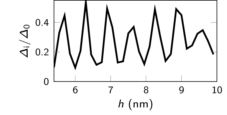
Another important effect arises from the finite height of the superconducting layer. Similar to semiconductor nanowires [38], the relative energy between the subbands within the superconducting layer and the TI nanowire subbands strongly impacts metallization and proximity effects. In particular, properties induced by the superconductor in the TI can be expected to oscillate as a function the layer height . For instance this is shown in Fig. 8 for the interior gap . Such oscillations occur with a period set by the Fermi wavelength of the superconductor (for our parameters nm). Although, due to disorder, one will observe some averaging of this effect, the oscillations of the TI nanowire properties due to small changes of layer thickness will likely make devices with consistent properties difficult to fabricate.
VI Discussion
We have investigated the impact of tunnel coupling a superconducting layer to a TI nanowire. In the strong coupling regime, where the proximity induced pairing potential is of the order of that found in the parent superconductor, we found a distinct phenomenology associated with the metallization effects due to the tunnel coupling. Although we find a subband-shift similar in size to the TI nanowire subband gap meV and a reduction of the magnetic field induced gap , these metallization effects are considerably smaller than the equivalents in semiconductors and can be mitgated relatively easily by gating or compensation. We also found that, in certain scenarios, metallization effects can actually be beneficial for inducing a topological superconducting phase, for instance the subband-splitting associated with the breaking of inversion symmetry by an applied gate voltage can actually be enhanced by a similar potential arising at the interface between the TI nanowire and superconductor.
Whilst metallization effects in TI nanowires do pose some experimental challenges we have shown that these can largely be mitigated during the device fabrication phase and do not present a significant roadblock to realizing MBSs. When compared to semiconductors, the reduced impact of a superconductor on the ability for a TI nanowire to realize topological superconductivity is a significant benefit, especially given recent developments in device fabrication and improvements of superconductor-TI interfaces [9].
The main remaining experimental challenge to achieve topological superconductivity and associated MBSs in TI nanowires is disorder. For instance it remains an open experimental question whether disorder, in particular, charged impurities in the bulk of TI nanowires [52, 53, 54, 55, 56, 57], will allow current TI nanowires to produce devices that can reliably and reproducibly realize MBSs. That said, the presence of a superconductor should help screen charged impurities and the large topological phase space for MBSs reduces constraints imposed by disorder. Nonetheless, the reduced metallization effects studied here and the large scope for further improvements of TI materials makes TI nanowires a very competitive platform to realize MBSs in the near term.
Acknowledgements.
We acknowledge useful discussions with Y. Ando, O. Breunig, and M. Rößler. This work was supported by the Georg H. Endress Foundation and the Swiss National Science Foundation and NCCR QSIT. This project received funding from the European Union’s Horizon 2020 research and innovation program (ERC Starting Grant, Grant No 757725).References
- Volovik [1999] G. Volovik, JETP Lett. 70, 609 (1999).
- Read and Green [2000] N. Read and D. Green, Phys. Rev. B 61, 10267 (2000).
- Kitaev [2001] A. Y. Kitaev, Phys. Usp. 44, 131 (2001).
- Ivanov [2001] D. A. Ivanov, Phys. Rev. Lett. 86, 268 (2001).
- Kitaev [2003] A. Y. Kitaev, Ann Phys 303, 2 (2003).
- Fu and Kane [2008] L. Fu and C. L. Kane, Phys. Rev. Lett. 100, 096407 (2008).
- Hasan and Kane [2010] M. Z. Hasan and C. L. Kane, Rev. Mod. Phys. 82, 3045 (2010).
- Sato and Ando [2017] M. Sato and Y. Ando, Rep. Prog. Phys. 80, 076501 (2017).
- Breunig and Ando [2021] O. Breunig and Y. Ando, Nature Reviews Physics (2021).
- Cook and Franz [2011] A. Cook and M. Franz, Phys. Rev. B 84, 201105(R) (2011).
- de Juan et al. [2019] F. de Juan, J. H. Bardarson, and R. Ilan, SciPost Phys. 6, 60 (2019).
- Legg et al. [2021a] H. F. Legg, D. Loss, and J. Klinovaja, Phys. Rev. B 104, 165405 (2021a).
- Peng et al. [2010] H. Peng, K. Lai, D. Kong, S. Meister, Y. Chen, X.-L. Qi, S.-C. Zhang, Z.-X. Shen, and Y. Cui, Nature Materials 9, 225 (2010).
- Hong et al. [2012] S. S. Hong, J. J. Cha, D. Kong, and Y. Cui, Nat. Commun. 3, 1 (2012).
- Hamdou et al. [2013] B. Hamdou, J. Gooth, A. Dorn, E. Pippel, and K. Nielsch, App. Phys. Lett. 103, 193107 (2013).
- Cho et al. [2015] S. Cho, B. Dellabetta, R. Zhong, J. Schneeloch, T. Liu, G. Gu, M. J. Gilbert, and N. Mason, Nat. Commun. 6, 1 (2015).
- Jauregui et al. [2015] L. A. Jauregui, M. T. Pettes, L. P. Rokhinson, L. Shi, and Y. P. Chen, Scientific Reports 5, 8452 (2015).
- Jauregui et al. [2016] L. A. Jauregui, M. T. Pettes, L. P. Rokhinson, L. Shi, and Y. P. Chen, Nat. Nano. 11, 345 (2016).
- Ziegler et al. [2018] J. Ziegler, R. Kozlovsky, C. Gorini, M.-H. Liu, S. Weishäupl, H. Maier, R. Fischer, D. A. Kozlov, Z. D. Kvon, N. Mikhailov, S. A. Dvoretsky, K. Richter, and D. Weiss, Phys. Rev. B 97, 035157 (2018).
- Rosenbach et al. [2020] D. Rosenbach, N. Oellers, A. R. Jalil, M. Mikulics, J. Kölzer, E. Zimmermann, G. Mussler, S. Bunte, D. Grützmacher, H. Lüth, and T. Schäpers, Advanced Electronic Materials 6, 2000205 (2020).
- Rosenbach et al. [2021a] D. Rosenbach, K. Moors, A. R. Jalil, J. Kölzer, E. Zimmermann, J. Schubert, S. Karimzadah, G. Mussler, P. Schüffelgen, D. Grützmacher, H. Lüth, and T. Schäpers, (2021a), arXiv:2104.03373 [cond-mat.mes-hall] .
- Münning et al. [2021] F. Münning, O. Breunig, H. F. Legg, S. Roitsch, D. Fan, M. Rößler, A. Rosch, and Y. Ando, Nature Communications 12, 1038 (2021).
- Legg et al. [2021b] H. F. Legg, M. Rößler, F. Münning, D. Fan, O. Breunig, A. Bliesener, G. Lippertz, A. Uday, A. A. Taskin, D. Loss, J. Klinovaja, and Y. Ando, (2021b), arXiv:2109.05188 [cond-mat.mes-hall] .
- Zhang and Vishwanath [2010] Y. Zhang and A. Vishwanath, Phys. Rev. Lett. 105, 206601 (2010).
- Bardarson et al. [2010] J. H. Bardarson, P. Brouwer, and J. Moore, Phys. Rev. Lett. 105, 156803 (2010).
- Chen et al. [2018] A. Q. Chen, M. J. Park, S. T. Gill, Y. Xiao, D. Reig-i Plessis, G. J. MacDougall, M. J. Gilbert, and N. Mason, Nature Communications 9, 3478 (2018).
- Jauregui et al. [2018] L. A. Jauregui, M. Kayyalha, A. Kazakov, I. Miotkowski, L. P. Rokhinson, and Y. P. Chen, Applied Physics Letters 112, 093105 (2018).
- Schüffelgen et al. [2019] P. Schüffelgen, D. Rosenbach, C. Li, T. W. Schmitt, M. Schleenvoigt, A. R. Jalil, S. Schmitt, J. Kölzer, M. Wang, B. Bennemann, U. Parlak, L. Kibkalo, S. Trellenkamp, T. Grap, D. Meertens, M. Luysberg, G. Mussler, E. Berenschot, N. Tas, A. A. Golubov, A. Brinkman, T. Schäpers, and D. Grützmacher, Nature Nanotechnology 14, 825 (2019).
- Kayyalha et al. [2019] M. Kayyalha, M. Kargarian, A. Kazakov, I. Miotkowski, V. M. Galitski, V. M. Yakovenko, L. P. Rokhinson, and Y. P. Chen, Phys. Rev. Lett. 122, 047003 (2019).
- Bai et al. [2020] M. Bai, F. Yang, M. Luysberg, J. Feng, A. Bliesener, G. Lippertz, A. A. Taskin, J. Mayer, and Y. Ando, Phys. Rev. Materials 4, 094801 (2020).
- Rosenbach et al. [2021b] D. Rosenbach, T. W. Schmitt, P. Schüffelgen, M. P. Stehno, C. Li, M. Schleenvoigt, A. R. Jalil, G. Mussler, E. Neumann, S. Trellenkamp, A. A. Golubov, A. Brinkman, D. Grützmacher, and T. Schäpers, Science Advances 7, eabf1854 (2021b).
- Bai et al. [2021] M. Bai, X.-K. Wei, J. Feng, M. Luysberg, A. Bliesener, G. Lippertz, A. Uday, A. A. Taskin, J. Mayer, and Y. Ando, (2021), arXiv:2108.08559 [cond-mat.mes-hall] .
- Fischer et al. [2021] R. Fischer, J. Picó-Cortés, W. Himmler, G. Platero, M. Grifoni, D. A. Kozlov, N. N. Mikhailov, S. A. Dvoretsky, C. Strunk, and D. Weiss, (2021), arXiv:2110.05143 [cond-mat.mes-hall] .
- Prada et al. [2020] E. Prada, P. San-Jose, M. W. de Moor, A. Geresdi, E. J. Lee, J. Klinovaja, D. Loss, J. Nygård, R. Aguado, and L. P. Kouwenhoven, Nat. Rev. Phys. 2, 575 (2020).
- Laubscher and Klinovaja [2021] K. Laubscher and J. Klinovaja, Journal of Applied Physics 130, 081101 (2021).
- Reeg and Maslov [2017] C. Reeg and D. L. Maslov, Phys. Rev. B 95, 205439 (2017).
- Reeg et al. [2017] C. Reeg, D. Loss, and J. Klinovaja, Phys. Rev. B 96, 125426 (2017).
- Reeg et al. [2018] C. Reeg, D. Loss, and J. Klinovaja, Phys. Rev. B 97, 165425 (2018).
- Antipov et al. [2018] A. E. Antipov, A. Bargerbos, G. W. Winkler, B. Bauer, E. Rossi, and R. M. Lutchyn, Phys. Rev. X 8, 031041 (2018).
- Woods et al. [2018] B. D. Woods, T. D. Stanescu, and S. Das Sarma, Phys. Rev. B 98, 035428 (2018).
- Mikkelsen et al. [2018] A. E. G. Mikkelsen, P. Kotetes, P. Krogstrup, and K. Flensberg, Phys. Rev. X 8, 031040 (2018).
- Středa and Šeba [2003] P. Středa and P. Šeba, Phys. Rev. Lett. 90, 256601 (2003).
- Klinovaja et al. [2012] J. Klinovaja, S. Gangadharaiah, and D. Loss, Phys. Rev. Lett. 108, 196804 (2012).
- Klinovaja and Loss [2013] J. Klinovaja and D. Loss, Phys. Rev. X 3, 011008 (2013).
- Bernevig et al. [2006] B. A. Bernevig, T. L. Hughes, and S.-C. Zhang, Science 314, 1757 (2006).
- Zhang et al. [2009] H. Zhang, C.-X. Liu, X.-L. Qi, X. Dai, Z. Fang, and S.-C. Zhang, Nat. Phys. physics 5, 438 (2009).
- Liu et al. [2010] C.-X. Liu, X.-L. Qi, H. Zhang, X. Dai, Z. Fang, and S.-C. Zhang, Phys. Rev. B 82, 045122 (2010).
- Ren et al. [2011] Z. Ren, A. A. Taskin, S. Sasaki, K. Segawa, and Y. Ando, Phys. Rev. B 84, 165311 (2011).
- Zhang et al. [2011] J. Zhang, C.-Z. Chang, Z. Zhang, J. Wen, X. Feng, K. Li, M. Liu, K. He, L. Wang, X. Chen, et al., Nat. Commun. 2, 1 (2011).
- Yang et al. [2015] F. Yang, A. A. Taskin, S. Sasaki, K. Segawa, Y. Ohno, K. Matsumoto, and Y. Ando, ACS Nano 9, 4050 (2015).
- Taskin et al. [2017] A. A. Taskin, H. F. Legg, F. Yang, S. Sasaki, Y. Kanai, K. Matsumoto, A. Rosch, and Y. Ando, Nature Communications 8, 1340 (2017).
- Skinner et al. [2013] B. Skinner, T. Chen, and B. Shklovskii, JETP 117, 579 (2013).
- Skinner and Shklovskii [2013] B. Skinner and B. I. Shklovskii, Phys. Rev. B 87, 075454 (2013).
- Borgwardt et al. [2016] N. Borgwardt, J. Lux, I. Vergara, Z. Wang, A. A. Taskin, K. Segawa, P. H. M. van Loosdrecht, Y. Ando, A. Rosch, and M. Grüninger, Phys. Rev. B 93, 245149 (2016).
- Knispel et al. [2017] T. Knispel, W. Jolie, N. Borgwardt, J. Lux, Z. Wang, Y. Ando, A. Rosch, T. Michely, and M. Grüninger, Phys. Rev. B 96, 195135 (2017).
- Bömerich et al. [2017] T. Bömerich, J. Lux, Q. T. Feng, and A. Rosch, Phys. Rev. B 96, 075204 (2017).
- Huang and Shklovskii [2021] Y. Huang and B. I. Shklovskii, Phys. Rev. B 104, 054205 (2021).