Compilation and scaling strategies for a silicon quantum processor
with sparse two-dimensional connectivity
Abstract
Inspired by the challenge of scaling up existing silicon quantum hardware, we investigate compilation strategies for sparsely-connected 2d qubit arrangements and propose a spin-qubit architecture with minimal compilation overhead. Our architecture is based on silicon nanowire split-gate transistors which can form finite 1d chains of spin-qubits and allow the execution of two-qubit operations such as Swap gates among neighbors. Adding to this, we describe a novel silicon junction which can couple up to four nanowires into 2d arrangements via spin shuttling and Swap operations. Given these hardware elements, we propose a modular sparse 2d spin-qubit architecture with unit cells consisting of diagonally-oriented squares with nanowires along the edges and junctions on the corners. We show that this architecture allows for compilation strategies which outperform the best-in-class compilation strategy for 1d chains, not only asymptotically, but also down to the minimal structure of a single square. The proposed architecture exhibits favorable scaling properties which allow for balancing the trade-off between compilation overhead and colocation of classical control electronics within each square by adjusting the length of the nanowires. An appealing feature of the proposed architecture is its manufacturability using complementary-metal-oxide-semiconductor (CMOS) fabrication processes. Finally, we note that our compilation strategies, while being inspired by spin-qubits, are equally valid for any other quantum processor with sparse 2d connectivity.
I Introduction
Qubit connectivity is a primary feature of any quantum computing technology. It represents the architectural arrangement of the qubits within the quantum processor and indicates the number of qubits with which any other qubit can interact. Highly-connected structures are favorable since two-qubit gates between arbitrary qubits require a smaller gate count and hence more complex problems can be solved with lower circuit depth. On the other hand, high qubit connectivity comes at the expense of technological complexity. Therefore, scaling while maintaining high-connectivity is a challenge being faced by many quantum computing technologies. All-to-all connectivity has been demonstrated by photonic Zhong2020 as well as ion-trap Linke2017 ; Pino:2021aa qubits, but the distributed nature of these technologies puts serious challenges on the path to scaling. On the other hand, solid-state systems, such as superconducting Arute2019 and quantum-dot spin qubits xue2021a , can exhibit 2d hardware topologies, which could be compactly integrated on a chip. This allows for colocating classical support electronics and offers an alternative path to scaling.
Implementations of 2d grids with nearest neighbor connectivity are desirable as this would allow for fault-tolerant quantum computing via the surface code Fowler2012 without additional gate overhead. However, scaling 2d nearest neighbor grids in solid-state systems poses substantial contact routing challenges and complicates the integration of classical support electronics in the qubit plane Charbon2016 ; Gonzalez-Zalba2020 . Quantum-classical integration would require levels of 3d integration unseen to date Veldhorst2017 . Therefore, solid-state platforms explore scaling with sparse 2d connectivity Vandersypen2017 ; Buonacorsi2019 ; Nation2021 and several works have explored optimized methods for running quantum algorithms on sparsely-connected hardware graphs Kivlichan2018 ; Guerreschi2018 ; Holmes2020 .
Particularly for the spin qubits, progress has been made in the last few years demonstrating high-fidelity gates Yoneda2017 ; Yang2019 and readout HarveyCollard2018 ; Urdampilleta2019 beyond the fault-tolerance threshold xue2021a ; noiri2021 ; mills2021 . Further, the first few qubit processors Zajac2017 ; Hendrickx2021 and blueprints Vandersypen2017 ; Veldhorst2017 ; Li2018 ; Boter2021 are beginning to emerge. Next steps will be focused towards scale-up, for which the use of industrial complementary metal-oxide-semiconductor (CMOS) processes is expected to play an important role Veldhorst2017 ; Gonzalez-Zalba2020 . In particular, modules containing industry-manufactured bilinear arrays of quantum dots (QDs) using split-gate nanowire transistor technology are readily manufactured and their qubit properties are widely being tested in experiments Betz2016 ; Hutin2019 ; Ansaloni2020 ; Chanrion2020 . These modules should provide a platform to demonstrate a 1d quantum processor in silicon which should allow for running early noisy intermediate-scale quantum (NISQ) algorithms Kivlichan2018 ; Cai2020 , Shor’s algorithm Fowler2004 or demonstrating logical qubits Jones2018 . How best scale this technology to allow for optimized operation of quantum algorithms with minimal compilation overhead is therefore an important question.
Here, we present a concept to utilize and scale QD chains of 1d split-gate transistors by combining them into 2d arrays with sparse connectivity. For this purpose, we introduce a new hardware junction which enables coupling between horizontally and vertically oriented arrays of split-gate transistors via spin shuttling Yoneda2021 . Given these hardware elements, we propose a modular 2d spin-qubit architecture with unit cells consisting of diagonally-oriented squares where nanowires form the edges and junctions the corners of a square. We then investigate compilation strategies for the proposed 2d architecture and demonstrate a square-root scaling of the compilation overhead, which outperforms the linear overhead of 1d devices, not only asymptotically, but also down to its smallest building block which is likely to be investigated first in future experiments. This allows for balancing the trade-off between compilation overhead and creating space in between the qubit modules which can be beneficial for colocation of classical control and readout electronics Vandersypen2017 ; Boter2019 ; Ruffino2021a and alleviating contact routing issues Veldhorst2017 ; Li2018 ; Schaal2019 ; Pauka2021 . Overall, this proposal should provide a compelling path to scaling, which could be manufactured with industrial CMOS processes.
II Results
II.1 Topology of the proposed architecture
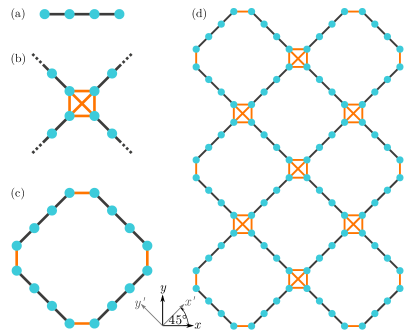
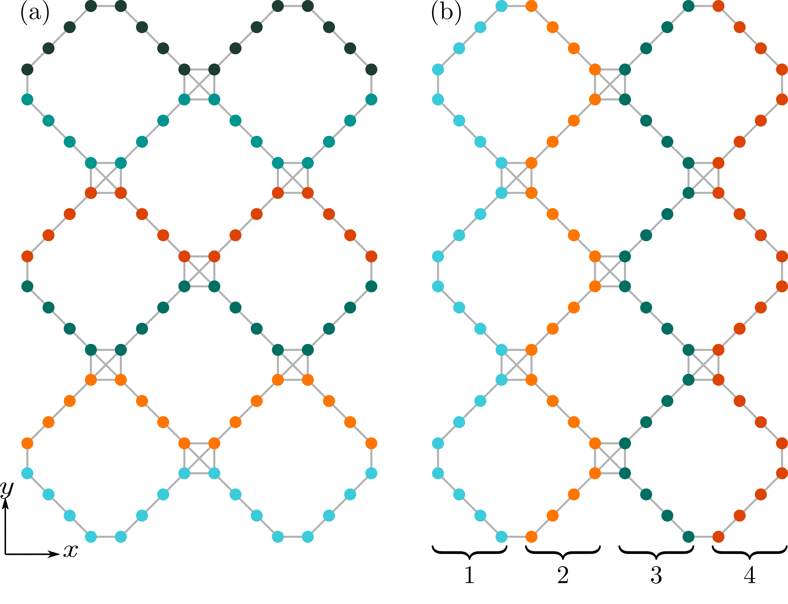
We start by introducing the hardware topology of the proposed architecture, before describing the detailed embodiment in silicon and discussing compilation strategies in subsequent sections. The core element of the architecture is a bilinear array of QDs using CMOS split-gate nanowire transistors. This gives rise to a 1d arrangement of qubits along a line, in which neighboring qubits can be involved in two-qubit operations as visualized in Fig. 1(a), where the dots indicate qubits and the black lines indicate possible two-qubit operations among neighbors. An additional building block is provided by a junction element which can join up to four linear segments in a perpendicular manner, as depicted in Fig. 1(b). In principle, a two-qubit operation can be executed between any two qubits involved in the junction as indicated by an orange line connecting the qubits. As explained in more detail in the following section, each two-qubit operation across the junction requires 6 additional spin shuttling steps. We consider the regime in which these coherent shuttling steps are fast, invoking negligible overhead as compared to the two-qubit operation. We note that each qubit can only be involved in a single two-qubit operation at a time.
The unit cell of the proposed architecture is then provided by squares, with linear segments along the edges and junctions at the corners of each square, as in Fig. 1(c). To form the complete architecture, we join squares in one direction and in the perpendicular direction. For convenience, we define the two directions as and . The complete architecture and and directions are show in Fig. 1(d). Since each square contains qubits and the device consists of squares, each device contains
| (1) |
qubits. We note that a crucial feature of the proposed architecture is the tilted orientation of squares at an angle of 45∘ in each unit cell, which minimizes the compilation overhead as will be explained later on.
II.2 Architecture embodiment in silicon
In the following, we introduce the embodiment of the proposed architecture in silicon and the corresponding control schemes in more detail. We focus on an implementation based on electron spins hosted in gate-defined QDs, but note that a similar proposal can be described for hole spin qubits. Readers interested only in the compilation techniques are advised to skip ahead.

Split-gate submodules
The principal building block of our proposal is the split-gate transistor Roche2012 ; Lundberg2020 ; Ansaloni2020 ; CirianoTejel2021 . It consists of an undoped silicon-on-insulator nanowire of height and width (typically 10 nm and 60 nm, respectively). The central part of the nanowire is gated by two metallic surface electrodes of length (typically 40-60 nm) which are isolated from the channel by the gate oxide (SiO2) of thickness (typically 6 nm); see Fig. 2(a). The gate stack is typically formed by 5 nm of TiN followed by 50 nm of polycrystalline silicon. The rectangular cross-section of the channel, as seen in Fig. 2(b), is covered by the pair of split gates which are separated by a face-to-face distance ( 30 nm) and enable local electrostatic control of the nanowire. At deep cryogenic temperatures, when positive voltages are applied to the gates, few-electron QDs form in the top-most corners of the device due to the corner effect Voisin2014 ; Ibberson2018 ; Ibberson2021 , as shown in Fig. 2(b). Charges can be drawn into the QDs from charge reservoirs formed of highly-doped silicon located at each side of the split gate.
The qubit that we consider here is the spin of a single electron (or hole) confined to one of the two corner dots in each split-gate transistor. The other spin is used as an ancilla for readout as described later on. To define the spin quantization axis, the structure is placed in a magnetic field. The architecture can be scaled-up by fabricating a series of split-gate transistors placed along the axis of the silicon nanowire, as depicted in Fig. 2(c). The split-gate edge-to-edge separation ( 40-60 nm) is set to enable sizable exchange coupling between spins, which we use to generate two-qubit interactions. Overall, the module results in a bilinear array of QDs. Given that the two QDs of each split-gate transistor encode one qubit – one dot contains a qubit spin and the other an ancilla spin for readout – the structure embodies a one-dimensional chain of silicon spin qubits of length , as described in the previous section.
Next, we explain control, readout and initialization of the 1d modules in detail. We base our explanation on the energy spectrum of the coupled two-spin system in the single spin basis as a function of the QD energy detuning, , and a finite magnetic field; see Fig 2(d). At large positive detuning with respect to the (11)-(20) charge hybridization point, the ground state of the system corresponds to the intradot singlet, . Here the () notation refers to the charge distribution among the two QDs, i.e. dots are occupied with and charges, respectively. At negative detuning, the ground state of the system is the (11) charge configuration whose spin degeneracy is broken by the external magnetic field. We consider the QDs have a tunnel coupling energy and present different -factors due to the variability of the Si/SiO2 interface Huang2017 , which further breaks the degeneracy of the and states. Here, the first spin refers to the spin with the lower -factor (see the Hamiltonian in Appendix A). Although not strictly necessary for the operation of the processor, we consider that larger Zeeman energy differences exist across the nanowire than along the nanowire, which could be achieved by creating an asymmetry in the gate structure. Using magnetic materials on the gate stack on one side of the split or placing the splits offset with respect to the nanowire axis Ibberson2021 may produce a difference in the Meissner effect at the location of the QDs. We use the energy spectrum to describe processes involving QDs within a split-gate and QDs on the same corner of the nanowire in different splits.
Initialization
We start with the 1d module loaded with one charge in each QD. Charges can be drawn in from reservoirs at the periphery following established methods Volk2019 . To initialize to a known spin state, QDs in each split gate are positively detuned until the system relaxes to the state (Fig. 2(e)). Then, the system is pulsed towards negative detuning adiabatically with respect to the - coupling, to initialize the QDs in the splits in the state (Fig. 2(f)).
Single-qubit operations
Electron spins in isotopically purified silicon present long coherence times ( s and ms) Veldhorst2014 . This enables high control fidelity via electron spin resonance (ESR) techniques Pla2013 ; Veldhorst2015 . Manipulation occurs for QDs on the same side of the nanowire which are now initialized to the state. Individual spin transitions can be addressed with an oscillatory magnetic field at frequency if in resonance with the Zeeman energy of the relevant spin transition (Fig. 2(g)). Typical Rabi frequencies achieved with this method are of the order of 1 MHz with fidelities in excess of % Yang2019 . The ESR implementation for the proposed architecture requires placing the structure inside a broadband 3D microwave cavity Vahapoglu2021 ; vahapoglu2021b .
The excitation is applied globally, and the qubits would be tuned in and out of resonance making use of the Stark shift using local voltage pulses at the qubit gate Laucht2015 . ESR allows two axis control (X and Y gates) by controlling the duration of the gate voltage pulses and the phase of the microwave excitation. Implementing the proposed architecture with hole-spin qubits, on the other hand, would result in shorter coherence times ( ns) Maurand2016 ; Camenzind2021 . However, the fact that holes exhibit larger spin-orbit coupling when compared to electron spins would allow for all-electrical control via the QD gates at relatively fast Rabi frequencies of up to 150 MHz via electric-dipole spin resonance (EDSR) Bosco2021 . We note that full control over the Bloch sphere of hole spins via X and Y rotations has been recently demonstrated with fidelities in excess of 99% Camenzind2021 .
Two-qubit operations
We propose engineering two-qubit gates between spins on the same corner of the nanowire by means of the spin-spin exchange interaction (Fig. 2(h)). The exchange interaction can be modulated electrostatically by applying a differential mode voltage on the two relevant neighboring gates that brings the system close to ; see Fig 2(d) and Fig 2(h). In the limit where the differential mode voltage pulse increases the exchange coupling beyond the Zeeman energy difference between spins, a or Swap gate can be implemented by timing the duration and depth of the interaction pulse Maune2012 ; He2019 . Alternatively, when the size of the modulation is smaller, such that the exchange coupling strength remains below the Zeeman energy difference, a CPhase gate could be implemented Veldhorst2015 with fidelity above fault-tolerant thresholds xue2021a ; noiri2021 ; mills2021 . In this article, we focus on the former gate but note that the Swap gate can be synthesized from a combination of CPhase and single qubit gates.
Readout
Spin readout is based on spin-dependent tunneling from the (11) to the (20) charge configurations, i.e. Pauli spin blockade Ono2002 . More particularly, the state is allowed to tunnel to the state, whereas all remaining two particle spins states are blocked Veldhorst2017 ; Zhao2019 ; see Fig 2(d) and (i). To detect this tunneling process, we suggest using dispersive readout GonzalezZalba2015 . One of the split gates is connected to a lumped-element electrical resonator which is driven at its natural frequency, . At , cyclic tunneling between the and , driven by the oscillatory resonator voltage, manifests in an additional quantum capacitance that loads the resonator producing a spin-dependent frequency shift that can be readily detected with standard methods Mizuta2017 ; Pakkiam2018 ; West2019 ; Zheng2019 ; Crippa2019 .
Junctions
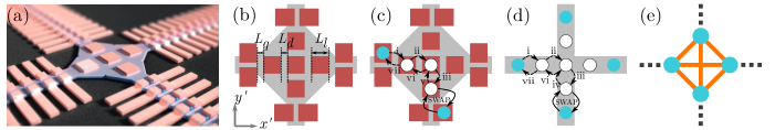
Next, we propose a new hardware junction which allows for coupling 1d submodules of split-gate transistors. The junction consists of etched silicon-on-insulator in quadrangular form, as can be seen in the central region of Fig. 3(a). The exact shape of the junction can vary to accommodate different levels of interconnection. Here, we present a square junction that enables connecting up to four submodules at an angle of 90∘, 180∘, or 270∘. On top of the junction, we place a series of metallic gates with the same gate stack as the split-gate transistors. We propose a five-gate structure arranged in cross geometry – one central square gate flanked by four square gates of the same footprint. The characteristic dimensions of the junction are indicated in Fig. 3(b), with submodule-to-edge-gate separation in () directions ( nm), the gate length in the () directions ( nm), and a junction gate-to-gate separation ( nm). The junction is invariant under rotations by 90∘.
The purpose of the junction is to create a shuttling path for electrons Mills2019 ; Yoneda2021 at the edges of the 1d submodules to be moved around the junction in the and directions on demand using the appropriate gate voltages sequence. These electrons can be moved to be in exchange coupling proximity with the electrons at the edge of another submodule where a two-qubit gate will be performed. We illustrate the operation of the junction using an coupling example in Fig. 3(c): (i) Shuttle the electron under the top-rightmost gate in the left module , to the left gate in the junction by applying a differential voltage between the two gates Yoneda2021 . (ii) Shuttle from the left gate to the central gate of the junction. (iii) Shuttle from the central gate to the bottom gate of the junction. (iv) Implement a two-qubit gate between the electron under the bottom gate in the junction and the electron under the left-topmost gate in the module, as described above. (v-vii) Shuttle the electron back following the reverse process. Finally, the abstracted hardware topology and the same shuttling sequence are presented in Fig. 3(d). Although in this work we consider two-qubit interactions between spins confined to different types of QDs (a corner QD in a submodule and a planar QD in the junction), the shuttling process above can be modified to produce two-qubit interactions between planar QDs which have been demonstrated Maune2012 ; Veldhorst2015 ; xue2021a ; noiri2021 . We consider the regime in which spin shuttling operations are performed coherently and much faster than the two-qubit operation in step (iv). In this case, the overhead is negligible and we use the simplified hardware topology given in Fig. 3(e). See Appendix B for a discussion of the different overhead regimes.
II.3 Compilation methods
We now present compilation methods for deploying quantum algorithms on the proposed architecture, following standard approaches. We assume that algorithms are given by a quantum circuit which consists of initialization, followed by a sequence of one- and two-qubit operations, and readout, suitable for execution on a fully-connected device. While most of these operations are readily available on the proposed architecture, the sparse connectivity will prohibit execution of two-qubit gates between arbitrary pairs of qubits that are not directly connected by an edge of the hardware graph. To address this issue, compilation methods re-express a given quantum circuit through an equivalent circuit readily amenable to the sparse hardware topology. More specifically, before executing a given two-qubit gate, one generally applies a sequence of Swap gates to shuttle the relevant qubits along the hardware graph until they reach neighboring positions. Once neighboring positions are reached, the two-qubit gate is executed and the sequence of Swap gates is reverted to promote the relevant qubits back to their original position. In applying this compilation strategy, the resulting quantum circuit accumulates a compilation overhead characterized by the number of additional Swap gates, , and the increased circuit depth, . Both quantities represent important quality metrics for the compilation which should be minimized to avoid additional decoherence and infidelities introduced through the additional Swap gates. We note that the proposed architecture uses two gates to implement the Swap operation.
In what follows, we focus on two major compilation scenarios: (I) The case of moving two arbitrary qubits together along the hardware graph. This covers the general case where each two-qubit operation is addressed individually and usually gives reasonable estimates for the compilation overhead. (II) The case of rearranging qubits in an arbitrary permutation. This compilation method is useful for variational algorithms Cerezo:2021aa from chemistry Peruzzo:2014aa ; fedorov2021vqe and finance ORUS which repeatedly execute some number of up to two-qubit operations in parallel. For such algorithms, the compilation must efficiently permute qubits into configurations which allow for executing the relevant two-qubit operations in parallel, even on the sparse hardware topology. To implement such permutations efficiently, one repeatedly applies a layer of Swap operations during which up to Swap gates are executed in parallel. Ultimately, this results in significantly lower circuit depth and reduced gate count than simply addressing each two-qubit operation individually.
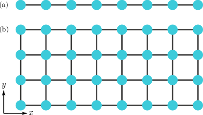
Finally, we compare our compilation methods to two important limiting cases – a 1d device which could be fabricated by joining nanowire submodules along one dimension, as depicted in Fig. 4(a), and a 2d rectangular device consisting of by qubits with nearest-neighbor connectivity, as depicted in Fig. 4(b).
II.3.1 Case I – Moving two qubits together along the shortest path

Algorithm
The compilation method for case I requires iterating over all two-qubit operations of a given input circuit and, for each pair of qubits involved in a two-qubit operation, (a) determining the shortest path connecting the two qubits and subsequently (b) executing Swap gates to connect the qubits along the shortest path, executing the two-qubit operation and shuttling qubits back to their original position. Finding the shortest path, i.e, the distance, between a pair of qubits can efficiently be implemented in polynomial time using, e.g., Dijkstra’s algorithm Cor2009 .
Overhead
The compilation overhead of this algorithm is determined by the length of the shortest path, , connecting the pair of qubits involved in each two-qubit operation along the hardware graph. In particular, the overhead of Swap gates accumulated per two-qubit gate is given by while the increased circuit depth per two-qubit operation will be given by , assuming that Swap gates on different pairs of qubits can be applied simultaneously.
Device specific overhead
To compare further the compilation overhead for different devices, we compute the average () and maximal () distances between qubit pairs in a given topology. For the linear layout with qubits, we have
| (2) |
For a rectangular grid of by qubits, we find that and and specifically for the square grid with we have
| (3) |
Finally, considering the proposed architecture for , the average and maximal qubit distances are
| (4) | ||||
For details of the derivation, see Appendix C.
We visualize the aforementioned compilation overheads expressed via mean and maximal qubit distances in Figs. 5(a) and 5(b) as a function of increasing qubit number. These figures illustrate several important properties, which we comment on in the following. The linear configuration (labeled 1D) clearly exhibits a linear scaling of the compilation overhead, while the rectangular device with nearest neighbor connectivity (labeled 2D) exhibits a square-root scaling. The compilation overhead of the proposed architecture inherits the favourable square-root scaling of 2d hardware topologies, making the proposed architecture favorable over 1d devices. Interestingly, the compilation overhead of the proposed device never exceeds the compilation overhead of the linear architecture, even for the smallest devices . This is useful as first experimental realizations of the proposed architecture would start from small prototypes. Finally, for increasing sparsity , the compilation overhead of the proposed architecture does increase; however, it never exceeds the overhead of the linear device. This allows for balancing the trade-off between compilation overhead and creating space in between the qubit modules which can be beneficial for colocation of classical support electronics.
II.3.2 Case II – Rearranging qubits in arbitrary permutations
We now consider the cost of permuting all qubits at once, making use of sorting networks hirata2011efficient ; Beals_2013 . We begin by recalling qubit permutations on linear and rectangular devices Steiger_2019 ; brierley2015efficient as these underlie the compilation method for the proposed sparse architecture.
Parallel neighbor sort for 1d
We first consider permutations on 1d linear devices with qubits using parallel neighbor sort habermann1972parallel , as depicted in Fig. 6(a). First, each node of the hardware graph is assigned an index in ascending order, and each qubit is labeled by its final position. Consecutive layers of Swap operations are then applied in up to steps. For odd steps , qubits on node pairs are compared and a Swap operation is applied if the final destination of qubit is larger than the final destination of qubit . For even steps , the same process occurs for qubits in node pairs . With this method, any permutation can be implemented in a maximum of layers leading to an increase in the circuit depth of
| (5) |
The maximum number of Swap operations needed is
| (6) |
An alternative is to use bubble sort or insertion sort, but the maximum depth increases to hirata2011efficient ; Beals_2013 .
Qubit permutation for the rectangular device
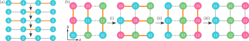
Next, we consider permutations on a rectangular device of qubits with nearest neighbor connectivity. We follow the algorithm of Ref. Steiger_2019 , which consists of the following three steps: (i) Rearrange the qubits in each column using parallel neighbor sort such that each row contains exactly one qubit with final destination in each column . (ii) Rearrange the qubits in each row using parallel neighbor sort such that all qubits are in the correct column. (iii) Rearrange the qubits in each column using parallel neighbor sort such that each qubit is in the correct final location. We note that column and row can also be interchanged in the above steps. An example visualizing the method is shown in Fig. 6(b).
Once step (i) provides an arrangement such that each row contains exactly one qubit with final destination in column , an implementation of steps (ii) and (iii) using parallel neighbor sort is simple. The challenge is to see that an efficient implementation of step (i) is always possible. This was shown in Refs. brierley2015efficient ; Steiger_2019 using Hall’s matching theorem hall1935representatives and will be discussed in more detail in its adaption to the proposed architecture with sparse 2d connectivity below. The overhead of the discussed method originates from consecutively using parallel neighbor sort on (i) columns (ii) rows and (iii) columns. This results in a maximum of
| (7) |
layers of Swap gates and
| (8) |
total Swap gates. Specifically, for the square , this gives
| (9) |
and
| (10) |
Generalized rows and columns
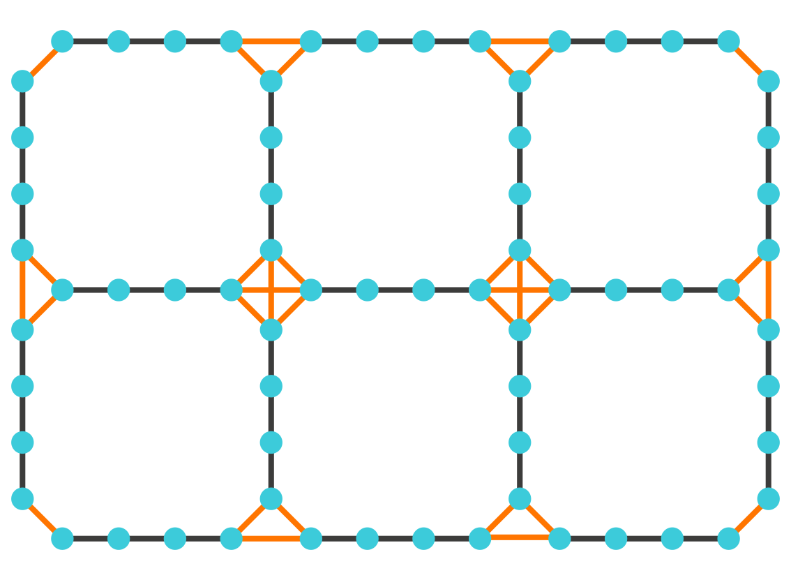
We now extend the method of Ref. Steiger_2019 to the proposed architecture with sparse 2d connectivity. Our method is based on the definition of generalized rows and columns as depicted in Figs. 7(a) and 7(b) respectively. In essence, this results in rows and columns with and qubits respectively, where any given row and column share qubits. Having defined these generalized rows and columns, we note that every qubit can conveniently be labeled by a combination of its column index, , and its vertical position, . Equivalently, we could choose to label a qubit by its row index, and its horizontal position, . The coordinates and can be seen in figure 1(d). We note that not all constructions of sparsely-connected devices from the linear segments and junction shown in figures 1(a) and 1(b) respectively would have enabled such simple definitions of generalized rows and columns. We show an alternative device construction in figure 8, for which equivalent generalized rows and columns do not exist. It is also not possible to draw a single line through all the qubits in such a device.
Compilation for the proposed architecture
With generalized rows and columns in place, we describe the corresponding compilation algorithm for implementing qubit permutations. Each qubit, in its initial location, carries a label , indicating its final position. An arbitrary qubit permutation can then be implemented using the following three steps: (i) Rearrange the qubits in each generalized column using parallel neighbor sort such that each set of qubits with fixed coordinate contains exactly one qubit with final destination in each column . (ii) Rearrange the qubits in each generalized row using parallel neighbor sort such that all qubits are moved into the correct column according to their column index . (iii) Rearrange the qubits in each generalized column using parallel neighbor sort such that each qubit is in the correct location along the columns. An example visualizing the method is given in Fig. 9.
Bipartite routing graph
We note again that, once step (i) provides an arrangement such that each set of qubits with vertical position contains exactly one qubit with final destination in column , an implementation of steps (ii) and (iii) using parallel neighbor sort is straightforward. The challenge is again to see that an efficient implementation of step (i) is always possible. The procedure to achieve this is illustrated in Fig. 9(e-g) and shall now be explained in more detail. To begin with, a bipartite graph of nodes is constructed, on the left and nodes on the right. Nodes on the left indicate columns in which a qubit is located initially. Nodes on the right indicate columns to which a qubit should be routed. To build the graph, one adds an edge to the bipartite graph for each qubit initially located in column and having final destination in column . An example is given in Fig. 9(e). We note that, since we have qubits located in each column initially and since we will have qubits with final destination located in each column, the bipartite graph has edges incident to each node. Since some qubits may originate and end up in the same column, the bipartite graph can have multiple edges connecting the same nodes.

Hall’s matchings
Next, to determine how qubits should be arranged along columns in step (i), one extracts perfect matchings with from the bipartite graph. A perfect matching is a set of edges such that each node of the bipartite graph is connected to exactly one edge of the matching. See Fig. 9(g) for examples showing one possible set of perfect matchings for the bipartite graph in Fig. 9(e). Finding perfect matchings for the given type of bipartite graph is always possible due to Hall’s matching theorem hall1935representatives . In the bipartite graphs that arise due to our compilation problem, each node has the same number of incident edges, a sufficient condition for Hall’s matching theorem to hold. Matchings can efficiently be found using the Ford-Fulkerson algorithm Cor2009 . To this end, one attaches virtual nodes and to all nodes on the left and right of the bipartite graph, respectively, and determines a minimal network flow from to ; see Fig. 9(f). Finding a minimal flow configuration reveals one matching at a time. Successively removing edges of a matching from the bipartite graph and repeatedly running the Ford-Fulkerson algorithm will reveal all matchings with , as visualized in Fig. 9(g). Finally, to route qubits in step (i), one selects qubits which move to vertical position by iterating over the edges of the th matching . Here, each edge signifies that in the generalized column a qubit destined for the generalized column should be moved to vertical position . Since edges in each set of matchings point to exactly one final destination per vertical position , the fact that matchings exist ensures that step (i) arranges the qubits in each column so that each row contains exactly qubits with final destination in column .
Compilation overhead
We close this section by evaluating the compilation overhead. Considering the succession of parallel neighbor sorts along (i) generalized columns of length , (ii) generalized rows of length , and (iii) again generalized columns of length , the maximum number of required layers of Swap gates is given by
| (11) |
and the maximum total number of Swap gates by
| (12) |
For the specific case , and using Eq. (1), we have
| (13) |
and
| (14) |
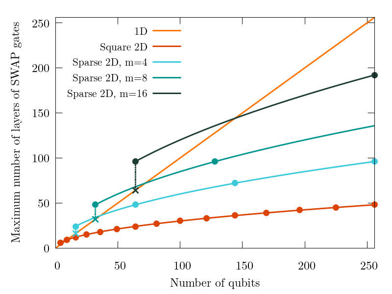
We compare the compilation overhead of the proposed architecture with sparse 2d connectivity to the linear and rectangular hardware graphs in Fig. 10. Again, the linear configuration (labeled 1D) exhibits a linear scaling of the compilation overhead, while the rectangular device with nearest neighbor connectivity (labeled 2D) exhibits a square-root scaling. The compilation overhead of the proposed architecture inherits the favourable square-root scaling of 2d hardware topologies, making the proposed architecture favorable over 1d devices. Interestingly, the compilation overhead of the proposed device never exceeds the compilation overhead of the linear architecture for . For device structures with , the compilation overhead of the proposed architecture can be reduced by recognising that the rearrangement of the sparse device can always be handled with a single parallel neighbor sort, by arranging the qubits along a single line. This ensures that the compilation overhead for the proposed architecture never exceeds the compilation overhead of the 1d architecture even for the smallest devices. This is useful as first experimental realizations of the proposed architecture would start from small prototypes. Finally, for increasing sparsity , the compilation overhead of the proposed architecture does increase; however, it again never exceeds the overhead of the linear device. This allows for balancing between compilation overhead and creating space in between the qubit modules which can be beneficial for colocation of classical support electronics.
III Discussion
Inspired by the challenge of scaling up existing silicon quantum hardware, we investigate compilation strategies for sparsely-connected 2d qubit arrangements and propose a spin-qubit architecture with minimal compilation overhead. Our considerations are inspired by silicon nanowire split-gate transistors which form finite 1d chains of spin-qubits, allowing for the execution of two-qubit operations such as Swap gates among neighbors. Adding to this, we describe a novel silicon junction which can couple up to four nanowires at one end into 1d or 2d arrangements via spin shuttling and Swap operations. Given these hardware elements, we propose a modular 2d spin-qubit architecture with unit cells consisting of diagonally-oriented squares with nanowires along the edges and junctions at the corners.
The junction geometry opens space between modules to route the gate lines and/or to place cryogenic classical electronics in the quantum processor plane Vandersypen2017 ; Boter2019 . Fabricating the qubits and the classical control layer using the same technology is appealing because it will facilitate the integration process, improving feedback speeds in error-correction protocols, and offer potential solutions to wiring and layout challenges Charbon2016 ; Franke2019 ; Xue2021 ; Park2021 ; Prabowo2021 ; Ruffino2021 . Integrating classical and quantum devices monolithically, using CMOS processes, enables the quantum processor to profit from the most mature industrial technology for the fabrication of large-scale circuits Ruffino2021a . We show that this architecture allows for compilation strategies which inherit the favourable square-root scaling of compilation overhead in 2d structure and outperform the best in class compilation strategy of 1d chains, not only asymptotically, but also down to the minimal structure of a single square. This result shows that scaling silicon nanowires into 2d structures will have benefits early on, even in experimental demonstrations of the smallest prototypes, thus encouraging building the proposed junction element and expanding silicon architectures into 2d arrangements. We further note that our compilation strategies, while being inspired by spin-qubits, are equally valid for any other quantum processor with sparse 2d connectivity.
The compilation strategies presented here act to demonstrate the square-root scaling in overhead due to routing for the sparsely-connected device, and the advantage of using this device over one with a 1d structure. Many other architecture-aware compilation methods exist and show good results (e.g., zulehner2018efficient, ; childs2019circuit, ; cowtan2019qubit, ; li2019tackling, ; lao2021timing, ). Circuit re-synthesis gheorghiu2020reducing provides another option. Alternatively, it may be beneficial to consider a compilation method designed with the desired algorithm in mind (e.g., Holmes2020, ; brownecompiler, ). However, the distance between qubits will clearly affect the overhead introduced through such compilation methods, and thus the results presented here provide some indication of their likely performance. Finally, the methods presented in this paper and discussed above are typically for NISQ-era devices; for the fault-tolerant era, it will clearly be important to investigate how best to perform error correction on the device.
III.1 Acknowledgments
We thank Michael A. Fogarty for his careful read of the manuscript. This research has received funding from the European Union’s Horizon 2020 Research and Innovation Programme under grant agreement No 688539 (http://mos-quito.eu) as well as grant agreement No 951852. This research has further received funding through the UKRI Innovate UK grant 48482 (NISQ.OS). MFGZ acknowledges support from UKRI Future Leaders Fellowship [grant number MR/V023284/1].
III.2 Competing Interests
The authors declare that they have no competing financial interests.
III.3 Correspondence
Correspondence and requests for materials should be addressed to O.C. (email: ophelia.crawford@riverlane.com) and M.F.G.Z (email: mg507@cam.ac.uk).
IV Appendix A. Two-spin Hamiltonian in a double quantum dot
To produce the energy spectrum in Fig. 2(d), we use the following Hamiltonian
| (15) |
where stands for the Zeeman energy average and is the Zeeman energy difference . Here is the g-factor of the particle , is the Bohr magneton and is the external magnetic field. We consider negligible coupling between spins states with different total spin number. This Hamiltonian is given in the basis states , assuming .
V Appendix B. Timescale of the shuttling sequence
For silicon electron spin qubits, coherent shuttling has been performed in 8 ns or longer Yoneda2021 . However, the lower end of this demonstration has been limited by the control hardware and hence faster coherent shuttling may be achieved. Considering state leakage due to non-adiabatic tunneling as the mechanism for loss of shuttling fidelity at short timescales, we estimate the minimum duration of the shuttling sequence. We consider the probability of a Landau-Zener transition
| (16) |
where is the driving velocity across the double QD anticrossing. Considering a minimum pulse amplitude of and GHz Yoneda2021 , we obtain a shuttling time, ps for . Considering 6 shuttling steps, the total shuttling time corresponds to ns.
Comparing this figure with the state-of-the-art exchange gate in silicon performed in subnanosecond timescales ( 0.8 ns) He2019 , there may be regimes in which shuttling time may add a sizable overhead. However, slower exchange gates (controlled by reducing the QD exchange coupling) or synthesized , from single qubit gates and a CPhase gate ( ns xue2021a ; noiri2021 ) may substantially increase the control fidelity. In that regime, shuttling time becomes negligible.
We note that the number of shuttling steps could be reduced to 4 by shuttling simultaneously two electrons and performing the SWAP gate when one electron is located under the central gate of the junction and the other under one of the neighboring gates.
VI Appendix C. Distance averaging
In this section, we will calculate the average distance between two qubits in different layouts by summing over all pairs of qubits and dividing by the total number of pairs of qubits. The average distance, , is therefore
| (17) |
where is the total distance between all pairs of qubits. We will make use of the standard sums, which are
| (18) | ||||
| (19) | ||||
| (20) | ||||
| (21) | ||||
| (22) |
VI.1 Sparsely-connected two-dimensional layout
We will find it useful to define the qubits by the particular square they are in, specified by an co-ordinate with possible values from 1 to and a co-ordinate with possible values from 1 to . We will use for these co-ordinates, and further use when considering two qubits simultaneously. We will then split the possible pairs of qubits into two – those with and those with .
In the calculations that follow, we will assume . A device can be rotated to ensure this is true.
VI.1.1 Pairs of qubits with
When considering these pairs of qubits, we split them again into those with and those with . We first consider the former. In this case, the shortest distance between any two vertices of the two chosen squares is . The shortest path between any one qubit in one square and any other qubit in the other square includes this shortest path between vertices. We will therefore begin by summing over the distances between the nearest vertices of the squares before later including the additional distance to the qubits.
We find that the total sum of distances between pairs of squares is given by
| (23) |
We now consider qubits with . In this case, the shortest distance between any two vertices of the two chosen squares is . Again, the shortest path between any one qubit in one square and any other qubit in the other square includes this shortest path between vertices. We will therefore now sum over the distances between the nearest vertices of the squares before later including the additional distance to the qubits. We find this total distance is given by
| (24) |
where
| (25) | ||||
| (26) | ||||
| (27) |
Evaluating these in turn, we find
| (28) |
| (29) |
| (30) |
We now have the total distance between all squares for which . As each square contains qubits, we first need to multiply these distances between the squares by . We also need to add the additional distance due to the fact the qubits are some distance from the vertex involved in the shortest distance between vertices. For each pair of squares, we therefore need to add the distance
| (31) |
The total number of pairs of squares is
| (32) |
The total number of pairs of squares with is
| (33) | ||||
| (34) | ||||
| (35) | ||||
| (36) |
Therefore, the total number of pairs of squares with is
| (37) |
The total distance between qubits for which is finally given by
| (38) |
VI.1.2 Pairs of qubits with
We now consider pairs of qubits with . In this case, there is not a unique pair of nearest vertices in the two squares and so we must consider different pairs of qubits in different manners.
We will consider squares with a particular value of in turn, giving us a line of diagonally oriented squares. For the moment, we assume that we have a set of such squares; we will sum over the different values of later. We first consider summing over the distances between all pairs of qubits down the sides of the squares, given by
| (39) |
We now consider pairs of qubits on opposite sides of the line of squares; however, to avoid double counting, we do not include pairs of qubits on opposite sides of the same square. This distance sum is given by
| (40) | ||||
| (41) | ||||
| (42) |
We next consider pairs of qubits where one of the pair is on one of the sides of the line of squares and the other is on an edge at right angles to this, on a ‘rung’ of the line of squares. Again, to avoid double counting, we exclude some pairs of qubits here. This sum of distances is given by
| (43) |
We finally consider pairs of qubits where both qubits are on a ‘rung’ of the line of squares. Here, the total distance between pairs of qubits is given by
| (44) |
Taking the sum , we find
| (45) |
We now need to sum over the different values of . There are four lines of squares for each and squares with . Therefore, the total distance between qubits with is
| (46) |
VI.1.3 Mean distance
The mean distance between two randomly selected qubits is given by
| (47) |
where we recall
| (48) |
VI.2 Linear layout
Given qubits laid out linearly, the average distance between a pair of qubits is
| (49) | ||||
| (50) | ||||
| (51) |
VI.3 Rectangular two-dimensional layout
Given a rectangle of qubits, the average distance between a pair of qubits is given by
| (52) |
and are the coordinates of two points. We sum over all possible and , and, to avoid double counting, sum over the distance between the point and any points on the same row and to the right, or on a higher row. The first term inside the brackets sums over those points to the right and on the same row or a higher row, whilst the second term sums over those points in the same column or to the left on a higher row. Rearranging terms, we find
| (53) |
and so
| (54) |
References
- (1) Zhong, H.-S. et al. Quantum computational advantage using photons. Science 370, 1460–1463 (2020).
- (2) Linke, N. M. et al. Experimental comparison of two quantum computing architectures. Proceedings of the National Academy of Sciences 114, 3305–3310 (2017).
- (3) Pino, J. M. et al. Demonstration of the trapped-ion quantum CCD computer architecture. Nature 592, 209–213 (2021).
- (4) Arute, F. et al. Quantum supremacy using a programmable superconducting processor. Nature 574, 505–510 (2019).
- (5) Xue, X. et al. Computing with spin qubits at the surface code error threshold. Preprint at https://arxiv.org/abs/2107.00628 (2021).
- (6) Fowler, A. G., Mariantoni, M., Martinis, J. M. & Cleland, A. N. Surface codes: Towards practical large-scale quantum computation. Phys. Rev. A 86, 32324 (2012).
- (7) Charbon, E. et al. Cryo-CMOS for quantum computing. In 2016 IEEE International Electron Devices Meeting (IEDM), 13.5.1–13.5.4 (2016).
- (8) Gonzalez-Zalba, M. F. et al. Scaling silicon-based quantum computing using cmos technology. Nature Electronics 4, 872–884 (2021). URL https://doi.org/10.1038/s41928-021-00681-y.
- (9) Veldhorst, M., Eenink, H. G. J., Yang, C. H. & Dzurak, A. S. Silicon CMOS architecture for a spin-based quantum computer. Nature Communications 8, 1766 (2017).
- (10) Vandersypen, L. M. K. et al. Interfacing spin qubits in quantum dots and donors–hot, dense, and coherent. npj Quantum Information 3, 34 (2017).
- (11) Buonacorsi, B. et al. Network architecture for a topological quantum computer in silicon. Quantum Science and Technology 4, 025003 (2019).
- (12) Nation, P., Paik, H., Cross, A. & Nazario, Z. The IBM Quantum heavy hex lattice. https://research.ibm.com/blog/heavy-hex-lattice (2021).
- (13) Kivlichan, I. D. et al. Quantum simulation of electronic structure with linear depth and connectivity. Phys. Rev. Lett. 120, 110501 (2018).
- (14) Guerreschi, G. G. & Park, J. Two-step approach to scheduling quantum circuits. Quantum Science and Technology 3, 045003 (2018).
- (15) Holmes, A., Johri, S., Guerreschi, G. G., Clarke, J. S. & Matsuura, A. Y. Impact of qubit connectivity on quantum algorithm performance. Quantum Science and Technology 5, 025009 (2020).
- (16) Yoneda, J. et al. A quantum-dot spin qubit with coherence limited by charge noise and fidelity higher than 99.9%. Nature Nanotechnology 13, 102–106 (2017).
- (17) Yang, C. H. et al. Silicon qubit fidelities approaching incoherent noise limits via pulse engineering. Nature Electronics 2, 151–158 (2019).
- (18) Harvey-Collard, P. et al. High-fidelity single-shot readout for a spin qubit via an enhanced latching mechanism. Phys. Rev. X 8, 021046 (2018).
- (19) Urdampilleta, M. et al. Gate-based high fidelity spin readout in a CMOS device. Nature Nanotechnology 14, 737–741 (2019).
- (20) Noiri, A. et al. Fast universal quantum control above the fault-tolerance threshold in silicon. Preprint at https://arxiv.org/abs/2108.02626 (2021).
- (21) Mills, A. R. et al. Two-qubit silicon quantum processor with operation fidelity exceeding 99% (2021).
- (22) Zajac, D. M. et al. Resonantly driven CNOT gate for electron spins. Science 359, 439–442 (2017).
- (23) Hendrickx, N. W. et al. A four-qubit germanium quantum processor. Nature 591, 580 – 585 (2021).
- (24) Li, R. et al. A crossbar network for silicon quantum dot qubits. Science Advances 4, eaar3960 (2018).
- (25) Boter, J. M. et al. The spider-web array–a sparse spin qubit array. Preprint at https://arxiv.org/abs/2110.00189 (2021).
- (26) Betz, A. et al. Reconfigurable quadruple quantum dots in a silicon nanowire transistor. Applied Physics Letters 108, 203108 (2016).
- (27) Hutin, L. et al. Gate reflectometry for probing charge and spin states in linear Si MOS split-gate arrays. In 2019 IEEE International Electron Devices Meeting (IEDM), 37–7 (2019).
- (28) Ansaloni, F. et al. Single-electron operations in a foundry-fabricated array of quantum dots. Nature Communications 11, 6399 (2020).
- (29) Chanrion, E. et al. Charge detection in an array of CMOS quantum dots. Physical Review Applied 14, 024066 (2020).
- (30) Cai, Z. Resource estimation for quantum variational simulations of the hubbard model. Physical Review Applied 14, 014059 (2020).
- (31) Fowler, A. G., Devitt, S. J. & Hollenberg, L. C. L. Implementation of Shor’s algorithm on a linear nearest neighbour qubit array. Quantum Info. Comput. 4, 237–251 (2004).
- (32) Jones, C. et al. Logical qubit in a linear array of semiconductor quantum dots. Physical Review X 8, 021058 (2018).
- (33) Yoneda, J. et al. Coherent spin qubit transport in silicon. Nature Communications 12, 4114 (2021).
- (34) Boter, J. M. et al. A sparse spin qubit array with integrated control electronics. In 2019 IEEE International Electron Devices Meeting (IEDM), 31–4 (IEEE, 2019).
- (35) Ruffino, A. et al. A cryo-cmos chip that integrates silicon quantum dots and multiplexed dispersive readout electronics. Nature Electronics (2021).
- (36) Schaal, S. et al. A CMOS dynamic random access architecture for radio-frequency readout of quantum devices. Nature Electronics 2, 236–242 (2019).
- (37) Pauka, S. J. et al. A cryogenic cmos chip for generating control signals for multiple qubits. Nature Electronics 4, 64–70 (2021).
- (38) Roche, B. et al. A tunable, dual mode field-effect or single electron transistor. Applied Physics Letters 100, 32103–32107 (2012).
- (39) Lundberg, T. et al. Spin quintet in a silicon double quantum dot: Spin blockade and relaxation. Physical Review X 10, 041010 (2020).
- (40) Ciriano-Tejel, V. N. et al. Spin Readout of a CMOS Quantum Dot by Gate Reflectometry and Spin-Dependent Tunneling. PRX Quantum 2, 010353 (2021).
- (41) Voisin, B. et al. Few-electron edge-state quantum dots in a silicon nanowire field-effect transistor. Nano Letters 14, 2094–2098 (2014).
- (42) Ibberson, D. J. et al. Electric-field tuning of the valley splitting in silicon corner dots. Applied Physics Letters 113, 53104 (2018).
- (43) Ibberson, D. J. et al. Large dispersive interaction between a CMOS double quantum dot and microwave photons. PRX Quantum 2, 020315 (2021).
- (44) Huang, W., Veldhorst, M., Zimmerman, N. M., Dzurak, A. S. & Culcer, D. Electrically driven spin qubit based on valley mixing. Phys. Rev. B 95, 75403 (2017).
- (45) Volk, C. et al. Loading a quantum-dot based “Qubyte” register. npj Quantum Information 5, 29 (2019).
- (46) Veldhorst, M. et al. An addressable quantum dot qubit with fault-tolerant control-fidelity. Nat Nano 9, 981–985 (2014).
- (47) Pla, J. J. et al. High-fidelity readout and control of a nuclear spin qubit in silicon. Nature 496, 334–338 (2013).
- (48) Veldhorst, M. et al. A two-qubit logic gate in silicon. Nature 526, 410–414 (2015).
- (49) Vahapoglu, E. et al. Single-electron spin resonance in a nanoelectronic device using a global field. Science Advances 7, eabg9158 (2021).
- (50) Vahapoglu, E. et al. Coherent control of electron spin qubits in silicon using a global field (2021). eprint 2107.14622.
- (51) Laucht, A. et al. Electrically controlling single-spin qubits in a continuous microwave field. Science Advances 1, e1500022 (2015).
- (52) Maurand, R. et al. A CMOS silicon spin qubit. Nature Communications 7, 1–6 (2016).
- (53) Camenzind, L. C. et al. A spin qubit in a fin field-effect transistor. Preprint at https://arxiv.org/abs/2103.07369 (2021).
- (54) Bosco, S., Hetényi, B. & Loss, D. Hole spin qubits in Si FinFETs with fully tunable spin-orbit coupling and sweet spots for charge noise. PRX Quantum 2, 010348 (2021).
- (55) Maune, B. M. et al. Coherent singlet-triplet oscillations in a silicon-based double quantum dot. Nature 481, 344–347 (2012).
- (56) He, Y. et al. A two-qubit gate between phosphorus donor electrons in silicon. Nature 571, 371–375 (2019).
- (57) Ono, K., Austing, D. G., Tokura, Y. & Tarucha, S. Current rectification by pauli exclusion in a weakly coupled double quantum dot system. Science 297, 1313–1317 (2002).
- (58) Zhao, R. et al. Single-spin qubits in isotopically enriched silicon at low magnetic field. Nature Communications 10, 5500 (2019).
- (59) Gonzalez-Zalba, M. F., Barraud, S., Ferguson, A. J. & Betz, A. C. Probing the limits of gate-based charge sensing. Nat Commun 6, 6084 (2015).
- (60) Mizuta, R., Otxoa, R., Betz, A. & Gonzalez-Zalba, M. Quantum and tunneling capacitance in charge and spin qubits. Physical Review B 95, 045414 (2017).
- (61) Pakkiam, P. et al. Single-shot single-gate rf spin readout in silicon. Phys. Rev. X 8, 41032 (2018).
- (62) West, A. et al. Gate-based single-shot readout of spins in silicon. Nature Nanotechnology 14, 437–441 (2019).
- (63) Zheng, G. et al. Rapid gate-based spin read-out in silicon using an on-chip resonator. Nature Nanotechnology 14, 742–746 (2019).
- (64) Crippa, A. et al. Gate-reflectometry dispersive readout and coherent control of a spin qubit in silicon. Nature Communications 10, 2776 (2019).
- (65) Mills, A. R. et al. Shuttling a single charge across a one-dimensional array of silicon quantum dots. Nature Communications 10, 1063 (2019).
- (66) Cerezo, M. et al. Variational quantum algorithms. Nature Reviews Physics 3, 625–644 (2021).
- (67) Peruzzo, A. et al. A variational eigenvalue solver on a photonic quantum processor. Nature Communications 5, 4213 (2014).
- (68) Fedorov, D. A., Peng, B., Govind, N. & Alexeev, Y. VQE method: A short survey and recent developments. Preprint at https:/arxiv.org/abs/2103.08505 (2021).
- (69) Orús, R., Mugel, S. & Lizaso, E. Quantum computing for finance: Overview and prospects. Reviews in Physics 4, 100028 (2019).
- (70) Cormen, T. H., Leiserson, C. E., Rivest, R. L. & Stein, C. Introduction to Algorithms (MIT Press, 2009), 3rd edn.
- (71) Hirata, Y., Nakanishi, M., Yamashita, S. & Nakashima, Y. An efficient conversion of quantum circuits to a linear nearest neighbor architecture. Quantum Information & Computation 11, 142–166 (2011).
- (72) Beals, R. et al. Efficient distributed quantum computing. Proceedings of the Royal Society A: Mathematical, Physical and Engineering Sciences 469, 20120686 (2013).
- (73) Steiger, D. S., Häner, T. & Troyer, M. Advantages of a modular high-level quantum programming framework. Microprocessors and Microsystems 66, 81–89 (2019).
- (74) Brierley, S. Efficient implementation of quantum circuits with limited qubit interactions. Preprint at https://arxiv.org/abs/1507.04263 (2015).
- (75) Habermann, A. N. Parallel neighbor-sort (or the glory of the induction principle) (1972).
- (76) Hall, P. On representatives of subsets. Journal of the London Mathematical Society 1, 26–30 (1935).
- (77) Franke, D. P., Clarke, J. S., Vandersypen, L. M. K. & Veldhorst, M. Rent’s rule and extensibility in quantum computing. Microprocessors and Microsystems 67, 1 – 7 (2019).
- (78) Xue, X. et al. CMOS-based cryogenic control of silicon quantum circuits. Nature 593, 205–210 (2021).
- (79) Park, J. S. et al. A fully integrated cryo-CMOS SoC for qubit control in quantum computers capable of state manipulation, readout and high-speed gate pulsing of spin qubits in Intel 22nm FFL FinFET technology. In 2021 IEEE International Solid- State Circuits Conference (ISSCC), vol. 64, 208–210 (2021).
- (80) Prabowo, B. et al. A 6-to-8GHz 0.17mW/qubit cryo-CMOS receiver for multiple spin qubit readout in 40nm CMOS technology. In 2021 IEEE International Solid- State Circuits Conference (ISSCC), vol. 64, 212–214 (2021).
- (81) Ruffino, A. et al. A fully-integrated 40-nm 5-6.5 GHz cryo-CMOS system-on-chip with I/Q receiver and frequency synthesizer for scalable multiplexed readout of quantum dots. In 2021 IEEE International Solid- State Circuits Conference (ISSCC), vol. 64, 210–212 (2021).
- (82) Zulehner, A., Paler, A. & Wille, R. An efficient methodology for mapping quantum circuits to the IBM QX architectures. IEEE Transactions on Computer-Aided Design of Integrated Circuits and Systems 38, 1226–1236 (2018).
- (83) Childs, A. M., Schoute, E. & Unsal, C. M. Circuit transformations for quantum architectures. Preprint at https://arxiv.org/abs/1902.09102 (2019).
- (84) Cowtan, A. et al. On the qubit routing problem. Preprint at https://arxiv.org/abs/1902.08091 (2019).
- (85) Li, G., Ding, Y. & Xie, Y. Tackling the qubit mapping problem for NISQ-era quantum devices. In Proceedings of the Twenty-Fourth International Conference on Architectural Support for Programming Languages and Operating Systems, 1001–1014 (2019).
- (86) Lao, L., van Someren, H., Ashraf, I. & Almudever, C. G. Timing and resource-aware mapping of quantum circuits to superconducting processors. IEEE Transactions on Computer-Aided Design of Integrated Circuits and Systems (2021).
- (87) Gheorghiu, V., Li, S. M., Mosca, M. & Mukhopadhyay, P. Reducing the CNOT count for Clifford+T circuits on NISQ architectures. Preprint at https://arxiv.org/abs/2011.12191 (2020).
- (88) Lao, L. & Browne, D. E. 2QAN: A quantum compiler for 2-local qubit Hamiltonian simulation algorithms. Preprint at https://arxiv.org/abs/2108.02099 (2021).