Insights to negative differential resistance in MoS2 Esaki diodes: a first-principles perspective
Abstract
\ceMoS_2 is a two dimensional material with a band gap depending on the number of layers and tunable by an external electric field. The experimentally observed intralayer band-to-band tunneling and interlayer band-to-band tunneling in this material present an opportunity for new electronic applications in tunnel field effect transistors. However, such a widely accepted concept has never been supported up by theoretical investigations based on first principles. In this work, using density functional theory, in conjunction with non-equilibrilibrium Green’s function techniques and our electric field gating method, enabled by a large-scale computational approach, we study the relation between band alignment and transmission in planar and side-stack \ceMoS_2 -- junction configurations. We demonstrate the presence of negative differential resistance for both in-plane and interlayer current, a staple characteristic of tunnel diode junctions, and analyze the physical origin of such an effect. Electrostatic potentials, the van der Waals barrier, and complex band analysis are also examined for a thorough understanding of Esaki Diodes.
I Introduction
Following the advent of the tunnel diode, new efforts emerged to identify candidate materials for such electronics. Discovered by Leo Esaki, these devices are valued for their possible applications in nanoscale circuitry Esaki (1958). Among these benefits is their usage in tunnel field effect transistors (TEFTs), which can have lower theoretical sub-threshold swing than traditional MOSFETs. The novel interlayer properties of atomically thin heterostructures have made such configurations attractive for TEFT operation. The advantage in heterojunction-based tunnel diodes is their difference in band structure between layers. External bias allows for programmable band alignment between layers, yielding nonlinear characteristics in band alignment. In particular, graphene and transition-metal dichalcogenides (TMDs) have been valued for their suitable dimensionality and electronic structure Britnell et al. (2012); Wang et al. (2017); Chen et al. (2017); Radisavljevic et al. (2011). One such TMD is \ceMoS_2, having a direct band gap in single layer configuration Mak et al. (2010).
Recent experiments have shown a highly tunable bandgap in bilayer \ceMoS_2 under external electric field Chu et al. (2015). Experimentally, there are difficulties in constructing heterojunctions using 2D TMDs as leads Kang et al. (2017). Semi-empirical studies have observed the presence of band-to-band tunneling in a nanoribbon under strain Ghosh and S. (2013). In addition, studies finding negative differential resistance in tunnel diode \ceMoS_2 systems are a fairly recent phenomenon, most being published within the past half-decade Nourbakhsh et al. (2016); Zhang et al. (2019). Within these studies, there has yet to be a comparison between planar and interlayer transport properties. A first-principles based investigation is necessary to fully understand the electronic processes and the effects of band to band tunneling in -- configuration \ceMoS_2 diodes. Before introducing our model for this study, we should mention that we previously have developed and applied first-principles methods to investigate field effects related to tunneling transistors Liu et al. (2020); Li et al. (2017). A number of systems were studied, focusing on different aspects of physical processes. Some other groups have also performed first-principles investigations to understand field effects in tunneling junctions Bani-Hashemian et al. (2016); Sohier et al. (2017); Brumme et al. (2014); however, this study is the first attempt that provides analysis of interlayer band-to-band tunneling in \ceMoS_2 bilayer systems in addition to a full analysis of band-to-band tunneling in a planar monolayer junction. The two types of junctions are prepared to separately quantify in-plane and interlayer tunneling. The rest of the paper is organized as follows: Section II describes theoretical approaches, computational details, and our simulation models; Section III presents our major results; and Section IV concludes our investigations with discussion of some important issues.
II Methods
All of our calculations used a first-principles approach. Transport calculations were performed using density functional theory Kohn and Sham (1965); Perdew et al. (1996), with non-equilibrium Green’s functions () techniques as implemented in TranSIESTA Brandbyge et al. (2002); Taylor et al. (2001), which accounts for core electrons via nonlocal, norm-conserving pseudopotentials Soler et al. (2002); Troullier and Martins (1991). The self-consistent field (SCF) approach yields the necessary Green’s functions to employ the Caroli formula for electron transmission Caroli et al. (1971); Meir and Wingreen (1992),
| (1) |
where and are advanced and retarded Green’s functions, respectively, and and represent the the level broadening functions for the right and left leads, respectively. This expression for the transmission function allows us to obtain the current across the scattering region via the usual Landauer equation Landauer (1957, 1970),
| (2) |
where and are the chemical potentials of the left and right reservoirs, and and are Fermi functions in the left and right leads. For the basis set, we use a double-zeta plus polarization (DZP) basis. We also employ the Monkhorst-Pack method for sampling -points in the Brillouin zone Monkhorst and Pack (1976). Our rectangular supercell uses a grid for SCF calculations and a grid for all transmission calculations. We set the convergence requirement for the probability density matrix to . Our functional for the exchange-correlation energy is within the generalized gradient approximation (GGA), specifically, the Perdew–Burke-Ernzerhof (PBE) form Perdew et al. (1996). The applicability of this functional to our systems will be discussed in a later section.
In the experiments led by Chen, the metal leads were made by gating \ceMoS_2 layers either positively or negatively Chu et al. (2015). In our simulation, we used doped leads, which are achieved by the virtual crystal approximation (VCA) as implemented in SIESTA. The VCA is a good approximation when the atomic number of the dopant atom is close to the atom it replaces, the doping concentration is relatively small, and wavefunctions spread over a large spatial region Elliott et al. (1974). We use neighboring atoms on the periodic table in our doping scheme to comply with the former restriction and choose the two elements Nb and Tc to mimic hole-doped and electron-doped \ceMoS_2, respectively. The very nature of the transport problem satisfies the latter. We apply this doping scheme to linearly shift the band structure of our leads, achieving the necessary non-equilibrium boundary conditions. However, the VCA cannot capture all the physics of random doping, which includes disordered scattering from random defects. Previous calculations show these effects on spin transport in nanojunctions Yan et al. (2018). Due to the non-linear changes to conductance arising from these effects, it is unclear to what degree the VCA causes an overestimation or underestimation of transmission at this particular doping concentration compared to random doping. For the purposes of our study, we use the VCA to model gated leads rather than randomly doped leads.
We calculated the complex band structure of pristine monolayer and bilayer \ceMoS2 using the PWCOND part Smogunov et al. (2004); Choi and Ihm (1999) of the Quantum ESPRESSO package Giannozzi et al. (2017, 2009). During self-consistent calculations with Quantum ESPRESSO, we utilized the PBE exchange correlation energy functional Perdew et al. (1996) together with projector augmented-wave (PAW) pseudopotentials Blochl (1994). The pseudopotentials were generated using the PSlibrary package version 1.0.0. Dal Corso (2014); Corso We applied and energy cutoffs for expanding the charge density and the wavefunctions respectively. The energy tolerance for self-consistency was set to . During complex band calculations with PWCOND, which is based on the self-consistent field previously found in Quantum ESPRESSO, we adopted an energy cutoff of for expanding the wavefunctions in two-dimensional planes as well. The number of subslabs was set to to ensure high accuracy.
III Results
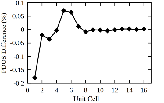
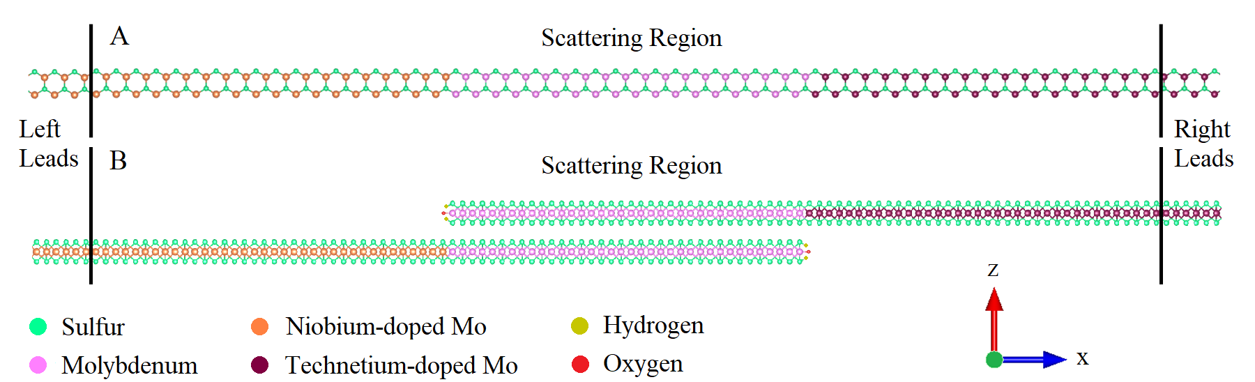
Figure 1A shows our monolayer structure that consists of a central pristine armchair \ceMoS_2 ribbon of 18 unit cells in width (or length in the transport direction), bracketed by 18 niobium- () or technetium-doped () \ceMoS_2 cells on each side and then by the two leads. The 18 unit cells right next to the pristine region or the scattering barrier serve as a buffer zone that screens charge accumulated next to the pristine region such that the whole scattering region is charge neutral. The pristine \ceMoS_2 ribbon has a finite band gap thus functioning as the tunneling barrier. The left and right leads are also \ceMoS_2 doped with Nb and Tc respectively to create a -- junction configuration. For this doping concentration, we performed a test for the screening length necessary for the transport calculation; we found that the size of the buffer zone is of adequate length to satisfy the charge neutrality condition and that the hopping parameters between the leftmost/rightmost unit cell in the buffer zone to the first unit cell of left/right lead is equal to the hopping between two adjacent unit cells in the left/right lead.
We analyzed the partial density of states (PDOS) according to
| (3) |
in which the Green’s function and level broadening functions are the same as those of the Caroli forumula. A detailed comparison of the PDOS of our buffer zone or depletion region and electrode is illustrated in figure 2. Such a comparison is necessary considering the need for exact matching of electronic density in the electrode and scattering region; this test indirectly verifies this agreement. It is clear that beyond 9 unit cells, the difference in the projected density of states between the buffer zone and a perfect lead is relatively small.
Figure 1B shows the configuration of our second junction. Compared to the planar configuration in Figure 1A, there is an overlapping region in the -direction that introduces a complexity in the junction and also allows interlayer electron tunneling. Again, the undoped insulating \ceMoS_2 functions as the tunneling barrier. The configurations of the two junctions allows us to separately quantify in-plane and interlayer transport properties. Previous experimental studies have used similar configurations with heterojunctions and homojunctions to study out-of-plane tunneling current Agarwal et al. (2014); Roy et al. (2015). Due to the sheared edge of the interlayer junction, hydrogen and oxygen serve as edge-terminating atoms. We will discuss edges and edge termination in a later section.
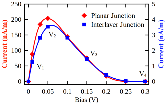
Figure 3 shows the calculated IV curves of both the planar and the side stacking or overlap junctions under low biases at room temperature. The characteristics of both graphs are similar, showing negative differential at biases higher than approximately . Above roughly , the current of both junctions drops by several orders of magnitude relative to the maximum current. These IV curves are consistent with that of an Esaki diode in forward bias mode, containing a local maximum at low bias followed by a negative differential resistance regime Esaki (1958). The current in the planar junction reaches a maximum value roughly 50 times that for the junction of the side stacking configuration, indicating the tunneling barrier across the two \ceMoS_2 layers interacting by van der Waals force is substantially higher than that across the the 18 unit cells of \ceMoS_2. Using partial density of states analysis, we can evaluate the band character of the junctions at biases of interest.
Using the GGA functional, we calculated the band-gap of monolayer \ceMoS_2 to be 1.59 eV. This result differs from the measured value of greater than 1.9 eV Mak et al. (2010). With such discrepancy, we expect an overestimation of tunneling current within our junctions. However, if the current arises from band to band tunneling effects, we do not expect the size of the band-gap to impact the overall character of our IV curve. This is due to band to band tunneling being driven by relative band alignment. Additionally, the measured band-gap of monolayer \ceMos_2 can vary as much as 1.39 to 2.16 eV due to environmental dielectric screening Ryou et al. (2016). The discrepancy between measured and our calculated band-gap is within this range of variations caused by environmental dielectric screening, which would be present in many electronic system. Thus, our calculated band-gap could coincide with the measured band-gap of monolayer \ceMos_2 in the presence of certain dielectrics. For these reasons, we believe that the GGA is sufficient for our calculations.
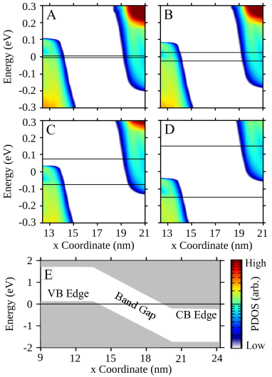
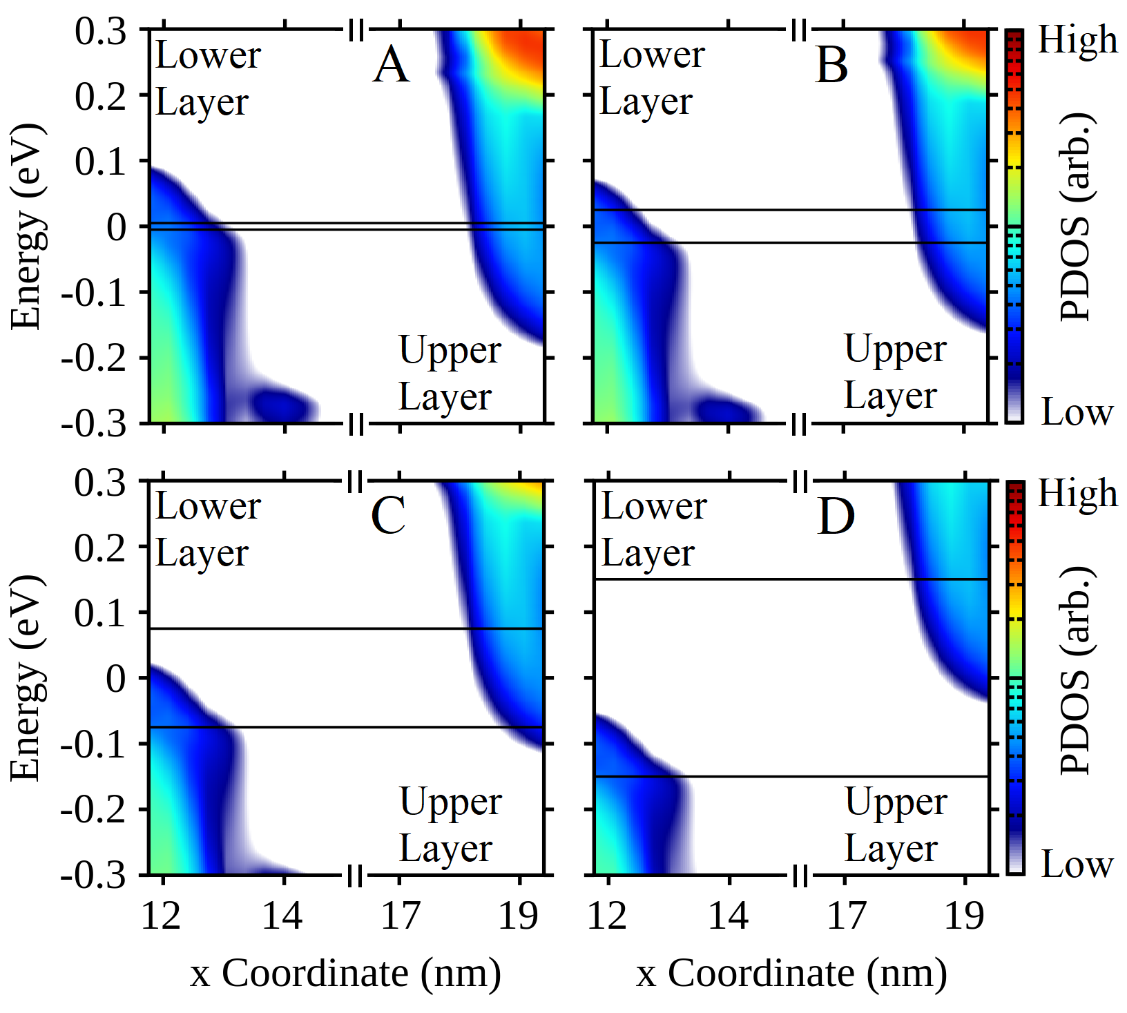
By plotting the PDOS of our planar junction at the biases of interest in Figure 4 as a function of position along transport direction and energy, we illuminate the transport properties of our systems. At V1, the valence bands of the left electrode and the conduction bands of the right electrode are well aligned; however, the bias window is relatively small. The bands remain well aligned at V2 with bias significantly increased. Further increases in bias skews band alignment, as seen in V3 and V4, with alignment completely lost at the latter bias. Band to band tunneling can no longer contribute to current for biases greater than V4. Band alignment within the bias window correlates with higher current, characteristic of an Esaki diode.
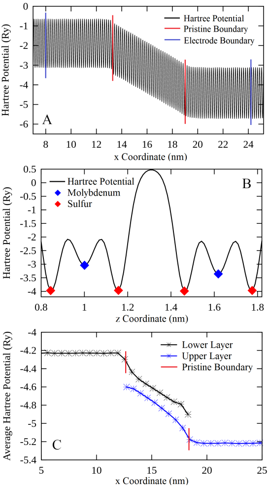
In Figure 5, we illustrate the PDOS as function of position and energy of the interlayer junction at the biases of interest. Comparison between PDOS and current indirectly shows intralayer and interlayer band to band tunneling across our junctions. Both planar and interlayer junctions share a similar character in density of states. However, the tunneling barriers are quite different. Figure 6 demonstrates this difference via the differing character of the Hartree potential between the junctions. The Hartree potential of the planar junction, seen in figure 6A, can be plotted along the transport direction without discontinuity. As illustrated in Figures 6B-C, the interlayer junction has a potential barrier corresponding to the van der Waals gap. Figure 6C shows the relative difference in Hartree potential between the two layers.
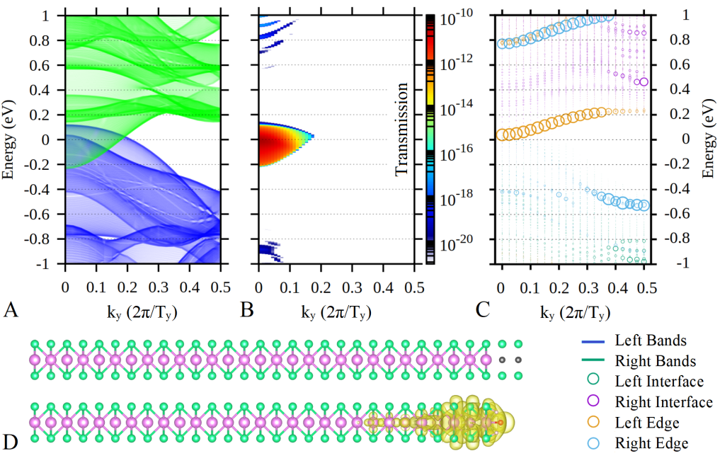
If band-to-band tunneling is the primary mechanism of transport across our junctions, we expect that transmission will coincide with the alignment of electrode bands. Comparison of both electrode band structure and the transmission function is seen in figure 8A-B. We see in the band structure of our electrodes an overlap around the Fermi energy; the broadest energy range of this overlap is at the point in the first Brillouin zone. Alongside this band structure is the transmission function of the interlayer junction plotted in a logarithmic scaling. We illustrate the correlation of electrode band crossing and transmission function by plotting both functions at the same energy and -path. Regions of highest band crossing coincide with regions of highest transmission.
Previous studies show the effects of edge \ceMoS_2 atoms on electronic structure Zhang et al. (2015). Charge accumulation on edge atoms leads to deviation from bulk electron density. In order to mitigate these effects, we follow the edge terminating structure of relaxing H and O onto bare \ceMoS_2. We analyze the contribution to local density of states (LDOS) of edge pristine \ceMoS_2 unit cells via fat bands. These are compared to the LDOS of the unit cells adjacent to doped \ceMoS_2 in Figure 8C. The edge unit cells show a high contribution to the density of states at the bottom of the conduction band. As these states fall within our bias window, we must ensure that edge states do not connect to the electrodes. In Figure 8D, we show the lowest energy, conduction band wavefunction of the lower-layer edge unit cell. This state corresponds to the highest local density of states near the Fermi energy on these edge atoms. We can see that the wavefunction does not connect to either electrode and is localized to the lower layer. Sampling other wavefunctions along the -path, we see that the states are likewise localized.
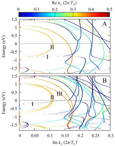
In order to understand the in-plane decay of the electron wave function into the intrinsic region of the two p-i-n junctions, we calculated the complex band structure of both monolayer and bilayer \ceMoS2. Fig. 7A shows the complex band structure of monolayer \ceMoS_2 to exhibit the evanescent states that decay in the transport direction of the planar junction. The reader may recall that the planar junction is in the - plane and electron transport is along the -direction. The wavevector for the periodic direction is set to zero here since the electron transmission at this point is highest at the Fermi energy. There are eight species of evanescent states at Fermi energy for , in which is the period of monolayer \ceMoS2 in the transport direction of the planar junction. Two of them consist of slowly decaying states near the top of the valence band or the bottom of the conduction band. They are marked as species I and II in Fig. 7A. Hereafter, a valence top refers to a local maximum of the valence band under the constraint that is zero, and similarly for a conduction bottom. This is for the convenience of describing the connectivity between complex bands and real bands. Species I derives from a valence top, and it is almost flat before . The band flatness indicates that this species quickly becomes quickly decaying states as the energy increases from the valence top. After , species I splits into two, an upper part and a lower part, with the upper part connecting to an unoccupied band much higher above the conduction bottom. Species II connects a valence top and a conduction bottom, enclosing an area over the band gap. This area is minimal among all areas that are enclosed by complex bands over the forbidden gap. Within the Wentzel–Kramers–Brillouin approximation, the band-to-band tunneling probability decays exponentially with such a minimum area. Harrison (1961); Khayer and Lake (2009)
Fig. 7B shows the complex band structure of a bilayer \ceMoS_2. In this case, there are three species of complex band which consist of slowly decaying states around the valence top or the conduction bottom. They are marked again by species I, II, and III in Fig. 7B. Species I of bilayer \ceMoS_2 is similar to species I of monolayer \ceMoS_2 in three aspects: 1) both of them are derived from the top of a valence band; 2) a single band splits into two bands at ; and 3) equals zero before the band splitting. Note that of bilayer \ceMoS2 is the same as that of monolayer \ceMoS2. Species II of bilayer \ceMoS_2 contains two copies of the dome-like complex band, each of which resembles species II of monolayer \ceMoS2. Species III of bilayer \ceMoS_2 is derived from the conduction bottom, and it extends into energies much lower than the valence top. For bilayer \ceMoS2, the minimum area of complex bands over the band gap is enclosed by both species I and II. When species I crosses species II, an electron may transit between the two species with the aid of phonons since the two species are different in crystal momentum and momentum is conserved during the transition. Phonon-assisted scattering may reduce the electron transmission and, thus, degrades the performance of the relevant electronic device. Luisier and Klimeck (2010)
IV Conclusion
We simulated armchair monolayer and interlayer \ceMoS_2 -- junctions consisting of doped \ceMoS_2 leads. Simulations were performed using in order to account for non-equilibrium conditions in the leads. Both junctions showed an initial positive differential resistance followed by a transition to negative differential resistance past a current maximum. Analysis of the partial density of states at different biases revealed a band alignment consistent with Esaki diode behavior. Furthermore, the band structures of both leads intersected at the same energy and -points comprising the transmission of the interlayer junction. These results confirm band to band tunneling as the primary mechanism of charge transfer in the low bias regime. Additionally, in-plane and interlayer band to band tunneling yields the same IV curve character, differing only in magnitude. However, the two junctions significantly differ in Hartree potential, the interlayer junction having a large tunneling barrier in the van der Waals gap. The planar junction, being continuous in the transport direction, has no such electrostatic barrier. Our complex band analysis reveals the slowest decaying evanescent states that contribute the most to the band-to-band tunneling probability. Phonon-assisted electron tunneling is more likely to occur in the interlayer junction than in the planar junction, degrading the performance of electronic devices based on bilayer \ceMoS2.
Due to the known issues with edge termination in \ceMoS_2 simulations, we used a H and O edge terminating scheme. The local density of states, obtained via fatband calculations, shows edge states near the Fermi energy. These states, however, are shown to have no effect on transport properties, as they are wholly localized to the edges of the interlayer junction.
Acknowledgements.
This work was supported by the US Department of Energy (DOE), Office of Basic Energy Sciences (BES), under Contract No. DE-FG02-02ER45995. Computations were done using the utilities of National Energy Research Scientific Computing Center and University of Florida Research Computing.References
- Esaki (1958) L. Esaki, Physical Review 109, 603 (1958).
- Britnell et al. (2012) L. Britnell, R. V. Gorbachev, R. Jalil, B. D. Belle, F. Schedin, A. Mishchenko, T. Georgiou, M. I. Katsnelson, L. Eaves, S. V. Morozov, N. M. R. Peres, J. Leist, A. K. Geim, K. S. Novoselov, and L. A. Ponomarenko, Science 335, 947 (2012), arXiv:1112.4999 [cond-mat.mes-hall] .
- Wang et al. (2017) Y.-P. Wang, J. N. Fry, and H.-P. Cheng, ACS Omega 2, 5824 (2017).
- Chen et al. (2017) G.-X. Chen, X.-G. Li, Y.-P. Wang, J. N. Fry, and H.-P. Cheng, Phys. Rev. B 95, 045302 (2017).
- Radisavljevic et al. (2011) B. Radisavljevic, A. Radenovic, J. Brivio, V. Giacometti, and A. Kis, Nature Nanotechnology 6, 147 (2011).
- Mak et al. (2010) K. F. Mak, C. Lee, J. Hone, J. Shan, and T. F. Heinz, Phys. Rev. Lett. 105, 136805 (2010), arXiv:1004.0546 [cond-mat.mtrl-sci] .
- Chu et al. (2015) T. Chu, H. Ilatikhameneh, G. Klimeck, R. Rahman, and Z. Chen, Nano Letters 15, 8000 (2015).
- Kang et al. (2017) S. Kang, X. Mou, B. Fallahazad, N. Prasad, X. Wu, A. Valsaraj, H. C. P. Movva, K. Kim, E. Tutuc, L. F. Register, and S. K. Banerjee, Journal of Physics D: Applied Physics 50, 383002 (2017).
- Ghosh and S. (2013) R. K. Ghosh and M. S., IEEE Trans. Electron Devices 60, 274 (2013).
- Nourbakhsh et al. (2016) A. Nourbakhsh, A. Zubair, M. S. Dresselhaus, and T. Palacios, Nano Letters 16, 1359 (2016).
- Zhang et al. (2019) R. Zhang, C. An, L. Xu, S. Wu, and D. e. a. Zhang, ACS Appl. Electron. Mater. 1, 523 (2019).
- Liu et al. (2020) S. Liu, Y. Xu, Y.-P. Wang, Y. P. Chen, J. N. Fry, and H.-P. Cheng, Applied Physics Letters 116, 031601 (2020).
- Li et al. (2017) X.-G. Li, Y.-P. Wang, X. G. Zhang, and H.-P. Cheng, arXiv , arXiv:1705.01205 (2017).
- Bani-Hashemian et al. (2016) M. H. Bani-Hashemian, S. Bruck, M. Luisier, and J. VandeVondele, Journal of Chemical Physics 144, 12 (2016).
- Sohier et al. (2017) T. Sohier, M. Calandra, and F. Mauri, Physical Review B 96 (2017), ARTN 075448 10.1103/PhysRevB.96.075448.
- Brumme et al. (2014) T. Brumme, M. Calandra, and F. Mauri, Physical Review B 89, 11 (2014).
- Kohn and Sham (1965) W. Kohn and L. J. Sham, Physical Review 140, 1133 (1965).
- Perdew et al. (1996) J. P. Perdew, K. Burke, and M. Ernzerhof, Phys. Rev. Lett. 77, 3865 (1996).
- Brandbyge et al. (2002) M. Brandbyge, J.-L. Mozos, P. Ordejón, J. Taylor, and K. Stokbro, Phys. Rev. B 65, 165401 (2002), arXiv:cond-mat/0110650 [cond-mat.mtrl-sci] .
- Taylor et al. (2001) J. Taylor, H. Guo, and J. Wang, Phys. Rev. B 63, 245407 (2001).
- Soler et al. (2002) J. M. Soler, E. Artacho, J. D. Gale, A. García, J. Junquera, P. Ordejón, and D. Sánchez-Portal, Journal of Physics: Condensed Matter 14, 2745 (2002).
- Troullier and Martins (1991) N. Troullier and J. L. Martins, Phys. Rev. B 43, 1993 (1991).
- Caroli et al. (1971) C. Caroli, R. Combescot, P. Nozieres, and D. Saint-James, Journal of Physics C: Solid State Physics 4, 916 (1971).
- Meir and Wingreen (1992) Y. Meir and N. S. Wingreen, Phys. Rev. Lett. 68, 2512 (1992).
- Landauer (1957) R. Landauer, IBM Journal of Research and Development 1, 223 (1957).
- Landauer (1970) R. Landauer, Philosophical Magazine 21, 863 (1970).
- Monkhorst and Pack (1976) H. J. Monkhorst and J. D. Pack, Phys. Rev. B 13, 5188 (1976).
- Elliott et al. (1974) R. J. Elliott, J. A. Krumhansl, and P. L. Leath, Reviews of Modern Physics 46, 465 (1974).
- Yan et al. (2018) J. Yan, S. Wang, K. Xia, and Y. Ke, Phys. Rev. B 97, 014404 (2018).
- Smogunov et al. (2004) A. Smogunov, A. Dal Corso, and E. Tosatti, Physical Review B 70, 9 (2004).
- Choi and Ihm (1999) H. J. Choi and J. Ihm, Physical Review B 59, 2267 (1999).
- Giannozzi et al. (2017) P. Giannozzi, O. Andreussi, T. Brumme, O. Bunau, M. B. Nardelli, M. Calandra, R. Car, C. Cavazzoni, D. Ceresoli, M. Cococcioni, N. Colonna, I. Carnimeo, A. Dal Corso, S. de Gironcoli, P. Delugas, R. A. DiStasio, A. Ferretti, A. Floris, G. Fratesi, G. Fugallo, R. Gebauer, U. Gerstmann, F. Giustino, T. Gorni, J. Jia, M. Kawamura, H. Y. Ko, A. Kokalj, E. Kucukbenli, M. Lazzeri, M. Marsili, N. Marzari, F. Mauri, N. L. Nguyen, H. V. Nguyen, A. Otero-de-la Roza, L. Paulatto, S. Ponce, D. Rocca, R. Sabatini, B. Santra, M. Schlipf, A. P. Seitsonen, A. Smogunov, I. Timrov, T. Thonhauser, P. Umari, N. Vast, X. Wu, and S. Baroni, Journal of Physics-Condensed Matter 29, 30 (2017).
- Giannozzi et al. (2009) P. Giannozzi, S. Baroni, N. Bonini, M. Calandra, R. Car, C. Cavazzoni, D. Ceresoli, G. L. Chiarotti, M. Cococcioni, I. Dabo, A. Dal Corso, S. de Gironcoli, S. Fabris, G. Fratesi, R. Gebauer, U. Gerstmann, C. Gougoussis, A. Kokalj, M. Lazzeri, L. Martin-Samos, N. Marzari, F. Mauri, R. Mazzarello, S. Paolini, A. Pasquarello, L. Paulatto, C. Sbraccia, S. Scandolo, G. Sclauzero, A. P. Seitsonen, A. Smogunov, P. Umari, and R. M. Wentzcovitch, Journal of Physics-Condensed Matter 21, 19 (2009).
- Blochl (1994) P. E. Blochl, Physical Review B 50, 17953 (1994).
- Dal Corso (2014) A. Dal Corso, Computational Materials Science 95, 337 (2014).
- (36) A. D. Corso, Welcome to pslibrary, https://dalcorso.github.io/pslibrary/, (2013).
- Momma and Izumi (2011) K. Momma and F. Izumi, Journal of Applied Crystallography 44, 1272 (2011).
- Agarwal et al. (2014) S. Agarwal, J. T. Teherani, J. L. Hoyt, D. A. Antoniadis, and E. Yablonovitch, IEEE Transactions on Electron Devices 61, 1599 (2014).
- Roy et al. (2015) T. Roy, M. Tosun, X. Cao, H. Fang, D.-H. Lien, P. Zhao, Y.-Z. Chen, Y.-L. Chueh, J. Guo, and A. Javey, ACS Nano 9, 2071 (2015).
- Ryou et al. (2016) J. Ryou, Y.-S. Kim, S. KC, and K. Cho, Scientific Reports 6, 29184 (2016).
- Zhang et al. (2015) L. Zhang, L. Wan, Y. Yu, B. Wang, F. Xu, Y. Wei, and Y. Zhao, The Journal of Physical Chemistry C 119, 22164 (2015).
- Harrison (1961) W. A. Harrison, Physical Review 123, 85 (1961).
- Khayer and Lake (2009) M. A. Khayer and R. K. Lake, Ieee Electron Device Letters 30, 1257 (2009).
- Luisier and Klimeck (2010) M. Luisier and G. Klimeck, Journal of Applied Physics 107, 6 (2010).