Controllable Nonreciprocal Optical Response and Handedness-Switching in Magnetized Spin-Orbit Coupled Graphene
Abstract
Starting from a low-energy effective Hamiltonian model, we theoretically calculate the dynamical optical conductivity and permittivity tensor of a magnetized graphene layer with Rashba spin-orbit coupling (SOC). Our results reveal a transverse Hall conductivity correlated with the nonreciprocal longitudinal conductivity. Further analysis illustrates that for intermediate magnetization strengths, the relative magnitudes of the magnetization and SOC can be identified experimentally by two well-separated peaks in the dynamical optical response (both the longitudinal and transverse components) as a function of photon frequency. Moreover, the frequency-dependent permittivity tensor is obtained for a wide range of chemical potentials and magnetization strengths. Employing experimentally realistic parameter values, we calculate the circular dichroism of a representative device consisting of magnetized spin-orbit coupled graphene and a dielectric insulator layer, backed by a metallic plate. The results reveal that this device has different relative absorptivities for right-handed and left-handed circularly polarized electromagnetic waves. It is found that the magnetized spin-orbit coupled graphene supports strong handedness-switchings, effectively controlled by varying the chemical potential and magnetization strength with respect to the SOC strength.
I Introduction
Graphene is a two-dimensional (2D) planar honeycomb arrangement of carbon atoms with one-atom thickness. The isolation of a graphene sheet was first officially reported in 2004.graphene This groundbreaking feat has inspired the isolation and creation of several novel single-layer materials that are one-atom thick, such as silicene and phosphorene, and has fueled the growth of a larger family of 2D materials.silicene ; phosphorene The most interesting electronics characteristics of graphene are accessible within a narrow energy window close to the Fermi level.RMP-2009-Neto The dispersion of quasiparticles near the Fermi level follows a linear relation as a function of momentum. This property facilitates the study of relativistic Dirac fermions within a practical platform. RMP-2008-Beenakker Additionally, graphene can withstand relatively high strains without rupturing, and supports a tunable chemical potential. These intriguing discoveries and advancements have made graphene attractive for both fundamental science and next-generation devices and technologies. RMP-2009-Neto ; G.G.Naumis ; S.Sarma
On its own, graphene has a negligible band gap and limited spin-related features such as magnetization and spin-orbit coupling (SOC) soc_intrinsic . Due to this, the use of free standing graphene in practical devices is still limited. To make graphene more suitable for technology-oriented applications and explore interesting fundamental phenomena, it is important to capitalize on additional effects such as the interplay of Dirac fermions with superconductivity, magnetization, and SOC. Along these lines, experimentally feasible approaches exp_f1 ; ex2 ; ex3 involve the exploitation of proximity effects, whereby the magnetism and SOC can be extrinsicallyrashba_gr2 induced into graphene by close contact with other materials D.Marchenko ; J.Balakrishnan ; A.Avsar ; prox4 ; Z.Wang . The proximity-induced magnetism and SOC in graphene is more appropriate than chemical doping as the former approach preserves the chemical properties of graphene and the quality of the graphene lattice remains nearly intact. D.Marchenko ; J.Balakrishnan ; A.Avsar ; prox4 ; Z.Wang This idea has driven numerous efforts both theoretically and experimentally to shed light on various aspects of superconducting gsuper ; halt2 magnetized mag_gr2 ; mag_gr1 ; rashba_gr , or spin-orbit coupled graphene rashba_gr ; equalspin3 ; equalspin4 ; soc_gr3 ; soc_gr4 .
On both the experimental and theoretical fronts, transport measurements have found excellent agreement with the low-energy effective models RMP-2009-Neto ; S.Sarma ; RMP-2008-Beenakker . Indeed, there have been several experiments carried out in this direction so far, reporting successful proximity-induced phenomena in graphene exp_f1 ; ex2 ; ex3 . Nonetheless, there is no clear-cut evidence and estimation of the type and strength of the induced SOC in graphene. For example, in Refs. exp_f1, ; ex2, ; ex3, , ferromagnetism was induced in graphene by placing it in close contact with yttrium iron garnet (YIG), which is a magnetic insulator with SOC. The corresponding signatures of the induced SOC and magnetization into graphene were observed through transverse Hall current measurements; however, a clear-cut picture of the type and strength of the SOC remains elusive.
When a plane circularly polarized electromagnetic (EM) wave interacts with some materials, there can be differences in the absorption of left-handed (LH) and right-handed (RH) circularly polarized light. When the absorptance of the incident circularly polarized beam depends on the handedness, the material possesses optical circular dichroism (CD) circD . Moreover, when tailor-made material platforms support “handedness-switching” under external controls, the system can change whether it predominately absorbs RH or LH polarized waves. The corresponding absorptance signatures can reveal valuable spin information and, possibly, intrinsic quantum details of the system circ1 ; circ2 ; circ3 . Such material platforms with nonzero intrinsic CD can be used in nanodevices as a circular polarization filter with atomic-scale control, and programmable optoelectronic devices with high-speed switching.
Having a low-power atomistic-scale mechanism to control electric-field rotation and absorption of EM waves is a desirable capability for modern integrated and compact optical nanodevices, sensors, and detectors I.K.Reddy ; L.D.Barron . Control of the polarization, phase, and magnitude of reflected and transmitted EM waves has been explored using metamaterials ws1 ; ws2 ; V.C.Nguyen ; S.Feng ; K.Halterman ; B.-X.Wang ; X.Wu ; K.Sonowal ; Q.Chen ; R.Sabri ; A.Forouzmand and patterned metasurfaces C.-C.Chang ; M.Barkabian ; M.Zare ; M.Nickpay ; P.Rezaei ; P.Zamzam ; H.Zhang ; L.Hu ; F.Li ; M.Amin . Nevertheless, fabrication challenges in creating metasurfaces, in addition to the low efficiency and limited compactness of the final structure, limit the effectiveness of this approach. Moreover, precise control over the dynamical and widely modulating system parameters is needed C.-C.Chang ; M.Barkabian ; M.Zare ; M.Nickpay ; P.Rezaei ; P.Zamzam ; H.Zhang ; L.Hu ; F.Li ; M.Amin , thus making atomic-scale optoelectronic elements with controllable material properties a more favorable alternative A.Y.Zhu .
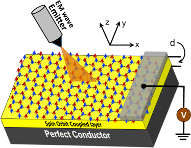
In this paper, we have considered a graphene layer with extrinsically induced Rashba SOC and magnetization. Starting from a microscopic Hamiltonian and employing a Green’s function approach, we derive expressions for the components of the dynamical optical conductivity tensor, and thereby obtain the associated frequency-dependent permittivity tensor. Our results illustrate that the optical conductivity acquires a strong peak associated with SOC at frequencies close to the corresponding SOC energy. A nonzero magnetization of moderate strength perpendicular to the graphene plane results in a clear second peak in the frequency-dependent optical conductivity, well separated from the SOC peak. To confirm our findings, we analyze their origins through visualizing various possible interband and intraband optical transitions in the band structure. Therefore, we find that the optical conductivity and dielectric response can be practical tools for identifying the presence of SOC induced in graphene, and estimating its strength unambiguously. Moreover, upon calculating the CD, we demonstrate that a nanoscale device of the type schematically shown in Fig. 1 can efficiently control handedness-switching by tuning the chemical potential and magnetization strength. Our results and findings may serve as a possible scenario for the physical origins of a nonzero CD observed in a recent experiment involving a graphene system deposited on a substrate C.Hwang . This would suggest that the interaction of graphene and a substrate can result in SOC and a nonzero magnetism.
The paper is organized as follows. In Sec. II, the theoretical model is outlined, including the model Hamiltonian. In Sec. III.1, the analytical and numerical evaluations of the dynamical optical conductivity are performed. In Sec. III.2, the finite-frequency dielectric tensor is discussed and the response of the magnetized spin-orbit coupled graphene to polarized EM waves is analyzed. Finally, we summarize the results with concluding remarks in Sec. IV.
II Formulation and framework
Graphene atoms are bonded through the -orbital electrons. The electronics consequences of these interactions for low energies close to the Fermi level can be properly described by a tight-binding model.RMP-2009-Neto The tight-binding model can be further simplified into an effective Hamiltonian model around the Fermi level without missing any important physics RMP-2009-Neto . Unlike the more complicated computational methods, the effective Hamiltonian model provides more clarity into the fundamental physics of systems. Also, it has long been proven that by contrasting results to experimental observations, the effective Hamiltonian captures the most interesting physics in graphene at low energies. RMP-2009-Neto ; S.Sarma ; RMP-2008-Beenakker Both magnetization and SOC can be extrinsically induced into graphene by virtue of the proximity effect involving the appropriate materials. exp_f1 ; ex2 ; ex3 The effective Hamiltonian of graphene with SOC and magnetization can be expressed as soc_gr1 ; soc_gr2 ,
| (1a) | |||
| (1b) | |||
The particles moving within the plane of graphene have momentum . The particles’ velocity at the Fermi level is approximately given by m/s. In this notation, and are vectors composed of Pauli matrices and refer to spin space and sublattice space, respectively. The honeycomb lattice of graphene is composed of ‘A’ and ‘B’ sublattices, as illustrated in Fig. 1. The strength of Rashba SOC, magnetization, and chemical potential are labeled by , h, and , respectively. In our calculations that follow, we have considered an arbitrary direction for the magnetization orientation so that . The magnetization might be induced into the graphene layer by a magnetized substrate such as YIG or the application of an external magnetic field exp_f1 ; ex2 ; ex3 . The intrinsic staggered SOC is negligibly small in a typical graphene layer, where the ratio of extrinsic to intrinsic SOC is on the order of 100 H.Min ; J.C.Boettger . However, since the magnetization can play the same role as this type of SOC RMP-2009-Neto ; S.Sarma , its presence can be revealed by subtle features in the response of graphene to RH and LH polarized waves. Thus, the overall effect on the results is similar to having present, even in situations where the intrinsic SOC is considerably large. The key features due the presence of magnetization are described below in detail. Hence, the associated field operators have four components, carrying the spin and sublattice degrees of freedom, i.e., and .
The components of the frequency-dependent permittivity tensor are related to the components of the conductivity tensor through the standard relations,
| (2a) | |||
| (2b) | |||
Here is the Kronecker delta, the indices run over , and is the permittivity of free space. The current-current correlation function is given by
| (3) |
Here are sublattice and spin degrees of freedom, respectively, and the components of the current operator are . The Fermi-Dirac function determines the temperature dependency () of optical conductivity and permittivity
| (4a) | |||
| (4b) | |||
in which is the Boltzmann constant.
III results and discussions
We first present results for the optical conductivity and analyze the physical origins of its various features in Sec. III.1. In Sec. III.2, the components of the dispersive permittivity tensor are studied as a function of chemical potential. Next, the effects of frequency, chemical potential, and magnetization on the circular dichroism of the device shown in Fig. 1 will be presented.
III.1 Finite-frequency optical conductivity and physical analysis
To obtain the permittivity tensor with frequency dispersion, the components of the Green’s function used in Eq. (II) need to be derived. For concreteness, and to simplify the expressions, we set in what follows. Nonetheless, we have obtained expressions for generic cases with . Using the low-energy Hamiltonian (1), the components of the Green’s function in the presence of an exchange field , and SOC are expressed by,
| (5a) | ||||
| (5b) | ||||
| (5c) | ||||
| (5d) | ||||
| (5e) | ||||
| (5f) | ||||
| (5g) | ||||
| (5h) | ||||
| (5i) | ||||
| (5j) | ||||
| (5k) | ||||
| (5l) | ||||
| (5m) | ||||
The other components of the Green’s function can be inferred from symmetry arguments. Substituting the Green’s function components into Eq. (2b), we find the following expression for the dynamical and components of optical conductivity:
| (6) |
where , and the definitions of are given in Appendix A. Here the symbol refers to the indices (), respectively. It is evident that owing to the complexities of these expressions, solutions can only be obtained numerically.
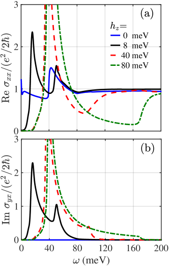
In Fig. 2, the real part of the longitudinal optical conductivity and imaginary part of the transverse optical conductivity are plotted as a function of the incident photon frequency . To this end, we have evaluated Eqs. (III.1), considering a situation where the magnetization is oriented along the axis, perpendicular to the plane of the graphene sheet, shown in Fig. 1. For this particular system, the following relations hold: and . The imaginary and real parts of and can be obtained by the Kramers-Kronig relationship. The components of the conductivity are normalized by the conductance unit . To facilitate the analysis of the optical conductivity, the chemical potential is set to zero, . Nevertheless, later the chemical potential shall be nonzero for illustrating its influence on the relevant material parameters. The strength of the SOC is set to meV, consistent with inferred values from experiments J.Balakrishnan , although our conclusions depend on the chemical potential and magnetization strength relative to . To perform numerically stable calculations, we have used the Lorentz model for the Dirac delta functions with narrow width, meV. We have also set the temperature to K in all subsequent calculations.
When meV in Fig. 2, the transverse conductivity vanishes. The longitudinal conductivity shows a weak Drude response at very low frequencies, . It is evident that peaks at meV and reaches the universal background conductivity, , at higher frequencies. When the magnetization is increased to a nonzero value, meV, two peaks in emerge at meV and meV, then decay at higher frequencies. The peaks observed in appear at the same frequencies for the longitudinal , and the conductivity approaches its background value for meV. Also, as seen, both the longitudinal and transverse conductivities are zero for small frequencies, meV. Increasing the magnetization to larger values, e.g., meV and meV, both the transverse and longitudinal components show that the magnitude of the first peak increases considerably whereas the second peak dampens out. The component shows a steep decline from meV for both meV and meV, before increasing again at meV and meV , respectively. Increasing the frequency higher results again in the longitudinal conductance leveling off at . Another important effect of the magnetization that can play a role in practical device applications is that within the low-frequency regime, the width of the zero conductance region can increase by increasing the magnetization strength to a threshold value.
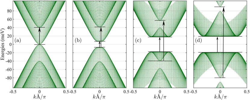
In order to gain further insight into the physical origins of the optical conductivity results above, we plot the associated band structures as a function of momentum in Fig. 3. For consistency, the values for the chemical potential and SOC strength are the same as those in Fig. 2. In Figs. 3(a)-3(d), the magnetization increases as meV, respectively. As seen in Fig. 3(a), in the presence of SOC, the bands associated with different spins are split by the amount meV at . Also, the valence band and conduction band just touch at and . The latter results in weak intraband transitions and a Drude response at meV, as observed in Fig. 2(a). The interband transitions occur at energies meV (shown by the arrow in Fig. 3(a)) and show up in the conductivity (Fig. 2(a)) as a peak at around meV. At high enough energies, the transition rate slows until finally reaching a constant rate equivalent to the universal conductivity . When the magnetization is increased to meV [Fig. 3(b)], a small energy gap ( meV) opens up in the band structure at the Fermi level, . There is also a slight shift upward of the second valence band. The interband transitions shown by the small and large arrows are the origins of the two peaks in the optical conductivity at approximately meV and meV, as seen in Fig. 2. The small gap ( meV) between the bottom of the conduction band and the top of the valence band prevents any transitions, and hence results in zero conductivity for frequencies less than meV [see Fig. 2].
Upon increasing the magnetization further to meV [Fig. 3(c)], the band gap widens to approximately meV, and the conduction band around acquires a dome-like segment with its top at meV from meV. The same feature occurs, but inverted, in the valence band. As shown by the small and large arrows, two types of interband transitions can be expected at meV and meV, respectively. These band structure transitions correlate with discernible features in the optical conductivity shown in Fig. 2. Finally, increasing the magnetization to meV [Fig. 3(d)] results in a band structure with similar features to those of meV shown in Fig. 3(c). Therefore, the associated optical conductivities are also similar. Another main feature found in both components of the optical conductivity is that when increasing , there is a considerable enhancement of the first peak. This can be understood by considering the corresponding band structures in Figs. 3(c) and 3(d), and comparing to Figs. 3(a) and 3(b), respectively. The bottoms of the valence and conduction bands become flattened and extended in Figs. 3(c) and 3(d), thus providing many more available states for interband transitions (as indicated by the small arrows).
III.2 Handedness switching and dielectric response
As seen in Fig. 2, the interplay of Rashba SOC and a magnetization perpendicular to the graphene film results in a strongly modified longitudinal optical conductivity, and generation of a finite transverse conductivity. The corresponding components of the permittivity tensor for graphene, , can thus be expressed as:
| (10) |
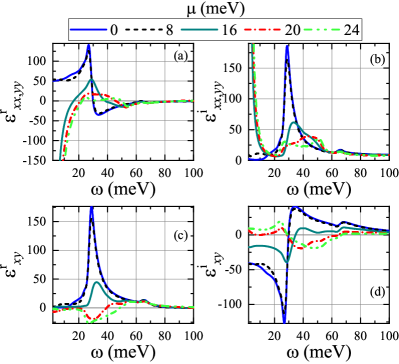
In Fig. 3, the behavior of the diagonal and off-diagonal components of are shown as a function of frequency. A representative set of parameter values are considered with the magnetization strength set at meV, and varies from - meV. The chemical potential is controllable via a gate voltage, as shown in Fig. 1. As discussed earlier and illustrated in, e.g., Fig. 4(c), for cases with and meV, the Fermi energy resides inside the gap of the band structure, and therefore only the interband transitions are allowed. For larger values of the chemical potential, i.e., meV, the intraband transitions are additionally allowed. The interband transitions are responsible for the Drude-like response at low frequencies in the longitudinal components of the dielectric response, i.e., . The Drude-like response to an electromagnetic wave can be clearly seen in Fig. 4(a) and Fig. 4(b) as . Considering the previous analysis of the components of the optical conductivity, which showed a strong frequency dependence for finite values of , it is evident that the large variations in the permittivity components are also strongly influenced by the presence of magnetization. Moreover, the frequency of the first peaks in Fig. 2 is directly related to the magnitude of the magnetization induced into graphene. As shown below, the strong transverse dielectric response seen in Figs. 4(c)-4(d), which reveals the presence of an extrinsically induced SOC in the graphene sheet (with no extrinsic SOC, the components vanish), is crucial for circular dichroism and polarization control.
Employing the computed frequency-dependent permittivity and conductivity tensors for various parameter sets, one now can easily study the absorption of EM waves from a hybrid device containing magnetized spin-orbit coupled graphene, such as the layered configuration shown in Fig. 1. This simple device consists of graphene sheet adjacent to a dielectric spacer layer with SOC (and possibly magnetization). The substrate consists of a reflective ground plate, which can be served by a metal, which will eventually be assumed to have perfect conductivity. The electric field component of the normally incident EM wave in the vacuum region is polarized in the plane, and we consider a circular polarization, so that the incident EM field components are out of phase, i.e., , for right-handed (), or left-handed () circular polarization. When determining how much of the incident EM energy is absorbed by the structure in Fig. 1, we invoke Maxwell’s equations. The equations, specific fields, and boundary conditions used for the results presented in the following can be found in Appendix B.
The fraction of energy that is absorbed by the system is determined by the absorptance : , where is the transmittance and is the reflectance, consistent with energy conservation. In determining the absorptance of the graphene system, we consider the time-averaged Poynting vector in the direction perpendicular to the interfaces (the direction), . We now take the limit of a metallic substrate, so there is no transmission of EM fields, and , and the tangential electric field at the spacer/metal boundary vanishes. Upon inserting the electric and magnetic fields for the vacuum region, we find,
| (11) |
Here we have normalized energy relative to the incident plane wave energy , where . The reflection coefficients are found upon using conditions (33)-(35). To quantify the effect that graphene has on the handedness of circularly polarized light, the quantity is introduced:
| (12) |
which describes the amount of circular dichroism through the difference in absorption of LH () and RH () circularly polarized EM waves. Therefore, indicates dominant right-handed absorption, while , indicates that left-handed polarization tends to be absorbed more.
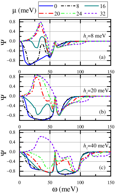
To evaluate the circular dichroism and handedness characteristics of the device shown in Fig. 1, the thickness of the spin-orbit coupled insulator layer (the yellow layer in Fig. 1) is set to a representative value of m, and the medium is assumed nondispersive. The latter assumption can be easily achieved with a large band gap semiconductor alloy, involving heavy elements to support SOC as well. The CD factor, , is shown in Fig. 5 as a function of the frequency of the incident EM wave. The legend shows the chemical potentials that are considered, with ranging from 0 to 32 meV, ensuring the most pertinent cases are shown. Additionally, each panel in Figs. 5(a)-5(c) considers a different finite value of the longitudinal magnetization , with meV, respectively. Beginning with Fig. 5(a), the results illustrate that at the charge neutrality point, , and moderate magnetization strength, there is strong circular dichroism, with the relative absorption favoring left-handed EM waves for a broad range of frequencies (). Increasing the chemical potential to meV yields larger variations in and a narrower frequency window for strong left-handed absorption. When the chemical potential is set to meV, gets shifted upward and oscillates about zero for frequencies lower than meV, resulting in left and right handedness switching as a function of frequency. Further increasing meV, results in for meV. At higher frequencies, , and levels off toward unity as vanishes [see Fig. 4], with both left-handed and right-handed polarizations absorbed equally. In Figs. 5(b) and 5(c), increasing the magnetization is shown to have a profound effect on the gate-controlled handedness-switching. This is seen in Fig. 5(b), where meV, and the optical response demonstrates an effectively larger circular dichroism over a wider frequency range. The results show that the relative absorption of left-handed and right-handed circularly polarized waves with these parameters can be manipulated through variations in frequency and chemical potential. Doubling the magnetization to meV [Fig. 5(c)] has a severe impact on the effectiveness of the device for handedness-switching of EM waves. Although at this larger magnetization the structure now exhibits circular dichrosim over a broader range of frequencies, is always negative or zero, except for the largest chemical potential, meV, where is positive (RH dominant) for meV. For all other values of shown, the LH polarization state always dominates ().
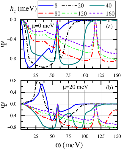
To explicitly show the influence of magnetization on CD, the factor against frequency for various values of is plotted in Fig. 6. Two values of the chemical potential are considered: (a) and (b) meV. As is clearly seen in Fig. 6(a), increasing the magnetization does not induce a sign change in , and hence there is no handedness-switching at the charge neutrality point, . Nonetheless, there are strong variations in and a dominant LH response over a frequency window that widens with increasing . Once the chemical potential is shifted away from the neutrality point, e.g., meV, Fig. 6(b) illustrates that now can induce handedness-switching. This switching is accessible for frequencies where meV and magnetizations meV. This trend has been found to continue for larger chemical potentials, whereby manipulating can increase the impact in calibrating and controlling the handedness-switching (not shown). Another feature that can be seen in Figs. 5 and 6 is the vanishing factor at specific frequencies. This follows from Eq. (36) and Eq. (38), where the reflectivity coefficients, when (for ). This is equivalent to having the spacer layer at the resonance width , where destructive interference occurs from reflected waves at both edges of the insulator layer ( is the wavelength of light in the insulator). This perfect reflectivity is most pronounced in Figs. 5(b)-5(c), and Fig. 6. From the resonance condition above, vanishes at ( is given in microns). Therefore, these specific frequencies depend solely on the material and geometrical characteristics of the spacer layer, and are independent of the dielectric response of the magnetized spin-orbit coupled graphene. Controlling the handedness of circularly polarized light with an external field offers several interesting possibilities for device applications. Through extensive parameter sweeps, general relationships between the magnetization, chemical potential, and frequency can be found at the crossover point, which can be beneficial for device fabrication. Although such an effort is outside the scope of this paper, we defer this interesting topic as a project for future works.
Note that there is no circular dichroism when the transverse components of the dielectric response are absent, i.e., . Therefore, a nonzero CD factor reveals important signatures involving the interplay of SOC and magnetization. Since the chemical potential of graphene is easily tunable by a gate voltage, the explored handedness-switching also demonstrates the extrinsically induced SOC and magnetization in graphene. On the technological side, this handedness-switching can be exploited for devising optoelectronic applications including chemical and biological sensors, where the corresponding polarization- and frequency-dependent absorption signatures can be controlled externally, e.g., by application of a gate voltage or magnetic field. The well-defined peaks in the absorption signatures were shown to provide a way to characterize the extrinsic SOC without ambiguity, as evidenced in the handedness-switching phenomenon and anomalous conductivity. Indeed, the magnitude of the extrinsic SOC can be estimated by the peaks in Fig. 2, as discussed above. If there is no magnetization, , the externally induced anomalous conductivity and handedness-switching disappears. Since the intrinsic SOC plays the same role as , its magnitude can be revealed using the same characterization techniques used above when the magnetization was present.
IV conclusions
In summary, we have studied the frequency-dispersive optical conductivity and associated dielectric response of magnetized graphene with Rashba spin-orbit coupling (SOC). Our results revealed that the strength and type of SOC can be unambiguously concluded and estimated through measurements of the frequency dependence of the optical conductivity. The band structure analysis illustrated that SOC and magnetization can generate two well-separated peaks in the conductivity, thus determining the strength of the SOC and magnetization. The transverse Hall conductivity, due to the interplay of magnetization and SOC, results in a nonzero circular dichroism. Exploring the permittivity tensor and conductivity, we studied the absorptance of a simple device, consisting of magnetized spin-orbit coupled graphene on top of an insulator layer and perfectly conducting metal substrate. Our findings showed that both the magnetization and chemical potential offer practical control mechanisms for handedness-switching and circular dichroism effects, where there is tunable absorption of left-handed and right-handed circularly polarized light. In addition, these findings offer a possible physical mechanism for recent experiments C.Hwang . Accordingly, the interaction of graphene and a substrate can be the source of SOC and magnetism in these platforms.
Acknowledgements.
Part of the calculations were performed using HPC resources from the DOD High Performance Computing Modernization Program (HPCMP). K.H. is supported in part by the NAWCWD In Laboratory Independent Research (ILIR) program and a grant of HPC resources from the DOD HPCMP.Appendix A Green’s functions and definition of parameters
In this appendix, we present the variables defined in the main text. Specifically, the variables , , in Eq. (III.1) are given by
| (13) |
| (14) |
| (15) |
| (16) |
| (17) |
| (18) |
| (19) |
| (20) |
| (21) |
| (22) |
The Dirac delta function is denoted by . Here we have considered to simplify the expressions. When all three components of the magnetization are nonzero and SOC is present, the resultant expressions become very lengthy, and thus they are not presented here.
If we set spin-orbit coupling to zero, i.e., , and all three components of the Zeeman field can be nonzero, i.e., , the Green’s functions reduce to
| (23a) | |||
| (23b) | |||
| (23c) | |||
| (23d) | |||
Substituting these Green’s functions (23a)-(23d) into Eq. (II), we find,
| (24) |
in which . Note that in the absence of SOC, the off-diagonal Green’s functions play no role in the optical conductivity and the transverse Hall components vanish altogether.
Appendix B Maxwell’s equation, EM fields, and boundary conditions
Assuming a harmonic time dependence for the EM field, we have:
| (25a) | ||||
| (25b) | ||||
where the integer denotes the region (0 for the vacuum, 1 for graphene, 2 for the insulator layer, and 3 for the metallic region). Combining Eqs. (25), we obtain,
| (26a) | ||||
| (26b) | ||||
where the free-space wave number is . For the nonmagnetic regions, we have . For the relative permittivity tensors, in the upper vacuum region, while the spacer layer is an isotropic dielectric with . The bottom region has (see Fig. 1).
For a normally incident EM wave, the electric field is written, , where the incident and reflected fields are expressed as , and , respectively. The spin-orbit coupling and static magnetic field generate off-diagonal components to the permittivity tensor in the graphene film. The reflected electric field has components, . Similarly, within the dielectric layer, the electric field is expressed as a superposition of upward and downward propagating waves: , where , , and . The transmitted field in the region below the spacer layer is , where (we later take the limit of a perfect metal in region 3). From Eq. (25b), the corresponding magnetic field in the vacuum region can be written , with
| (27a) | |||
| (27b) | |||
| (27c) | |||
where is the impedance of free space. The magnetic field in the dielectric region can be decomposed as , where
| (28a) | |||
| (28b) | |||
Here is the impedance of the dielectric layer, and for the metal region.
The presence of graphene enters in the boundary condition for the tangential components of the magnetic field by writing
| (29) |
where is the normal to the vacuum/graphene interface, and is the current density at the interface. Thus, we have
| (30) | ||||
| (31) |
where we used Ohm’s law to connect the surface current density to the electric field: . Note that one can also consider the graphene layer as a finite-sized slab, like the spacer layer, and using the dielectric response tensor discussed earlier, solve for the fields within the graphene layer (for continuity, the calculations are not shown here). We have found that this approach leads to equivalent results, but treating the graphene layer as a current sheet with infinitesimal thickness leads to simpler expressions. Hence, we follow the latter approach. We also have for the electric field at the graphene interface
| (32) |
Upon matching the tangential fields at the vacuum/graphene and dielectric/substrate interfaces, we have the following conditions:
| (33) | ||||
| (34) |
while matching the tangential fields at the dielectric/substrate interface gives
| (35) |
Appendix C Calculation of electromagnetic field coefficients
In the limit of a perfectly conducting substrate, the electric field in the spacer region can be written simply as . The coefficients for the electromagnetic fields in the spacer and vacuum regions are found by implementation of the appropriate boundary conditions discussed above. We subsequently find the respective components of the reflection coefficient, and electric field component in the spacer layer to be
| (36) |
and,
| (37) |
Here we have defined . The reflection coefficient for the incident electric field in the direction is found through the relationship
| (38) |
Similarly, the electric field coefficients for the spacer region are related via
| (39) |
As the expressions above show, the crucial difference in the coefficients for the RH and LH polarizations is the term arising from the SOC and Zeeman field induced in the graphene layer.
References
- (1) K. S. Novoselov, A. K. Geim, S. V. Morozov, D. Jiang, Y. Zhang, S. V. Dubonos, I. V. Grigorieva, A. A. Firsov, Electric Field Effect in Atomically Thin Carbon Films, Science. 306, 666 (2004); J.C. Meyer, A.K. Geim, M.I. Katsnelson, K.S. Novoselov, T.J. Booth, S. Roth, The structure of suspended graphene sheets, Nature 446, 60 (2007).
- (2) B. Aufray, A. Kara, S. B. Vizzini, H. Oughaddou, C. LeAndri, B. Ealet, G. Le Lay, Graphene-like silicon nanoribbons on Ag(110): A possible formation of silicene, App. Phys. Lett. 96,183102 (2010).
- (3) H. Liu, A. Neal, Z. Zhu, Z. Luo, X. Xu, D. Tomanek, P. Ye, D. Peide, Phosphorene: An Unexplored 2D Semiconductor with a High Hole Mobility, ACS Nano. 8, 4033 (2014).
- (4) A. H. Castro Neto, F. Guinea, N. M. R. Peres, K. S. Novoselov, and A. K. Geim, The electronic properties of graphene, Rev. Mod. Phys. 81, 109 (2009).
- (5) C. W. J. Beenakker, Andreev reflection and Klein tunneling in graphene, Rev. Mod. Phys. 80, 1337 (2008).
- (6) S. Das Sarma, S. Adam, E. H. Hwang, and E. Rossi, Electronic transport in two-dimensional graphene, Rev. Mod. Phys. 83, 407 (2011).
- (7) G. G. Naumis et al, Electronic and optical properties of strained graphene and other strained 2D materials: a review, Rep. Prog. in Phys. 80, 096501 (2017).
- (8) Hongki Min, J. E. Hill, N. A. Sinitsyn, B. R. Sahu, Leonard Kleinman, and A. H. MacDonald, Intrinsic and Rashba spin-orbit interactions in graphene sheets, Phys. Rev. B 74, 165310 (2006).
- (9) Z. Wang, C. Tang, R. Sachs, Y. Barlas, J. Shi, Proximity-induced ferromagnetism in graphene revealed by the anomalous Hall effect, Phys. Rev. Lett. 114, 016603 (2015).
- (10) J. B. S. Mendes, O. Alves Santos, L. M. Meireles, R. G. Lacerda, L. H. Vilela-Leao, F. L. A. Machado, R. L. Rodriquez-Suares, A. Azevedo, and S. M. Rezende, Spin-Current to Charge-Current Conversion and Magnetoresistance in a Hybrid Structure of Graphene and Yttrium Iron Garnet, Phys. Rev. Lett. 115, 226601 (2015).
- (11) S. Dushenko, H. Ago, K. Kawahara, T. Tsuda, S. Kuwabata, T. Takenobu, T. Shinjo, Y. Ando, and M. Shiraishi, Gate-Tunable Spin-Charge Conversion and the Role of Spin-Orbit Interaction in Graphene, Phys. Rev. Lett. 116, 166102 (2016).
- (12) E. I. Rashba, Graphene with structure-induced spin-orbit coupling: Spin-polarized states, spin zero modes, and quantum Hall effect, Phys. Rev. B 79, 161409(R) (2009).
- (13) D. Marchenko, A. Varykhalov, M. R. Scholz, G. Bihlmayer, E. I. Rashba, A. Rybkin, A. M. Shikin, and O. Rader, Giant Rashba splitting in graphene due to hybridization with gold, Nature Commun. 3, 1232 (2012).
- (14) J. Balakrishnan, G. K. W. Koon, M. Jaiswal, A. H. Castro Neto and B. Ozyilmaz, Colossal enhancement of spin–orbit coupling in weakly hydrogenated graphene, Nat. Phys. 9, 284287 (2013).
- (15) A. Avsar, et. al., Spin–orbit proximity effect in graphene, Nat. Comm., 5, 4875 (2014).
- (16) Z. Wang, D.–K. Ki, H. Chen, H. Berger, A. H. MacDonald, and A. F. Morpurgo, Strong interface-induced spin–orbit interaction in graphene on , Nat. Comm. 6, 8339 (2015).
- (17) T. Wakamura, F. Reale, P. Palczynski, S. Gueron, C. Mattevi, and H. Bouchiat, Strong Anisotropic Spin-Orbit Interaction Induced in Graphene by Monolayer WS2, Phys. Rev. Lett. 120, 106802 (2018).
- (18) M. Ben Shalom, M. J. Zhu, V. I. Fal’ko, A. Mishchenko, A. V. Kretinin, K. S. Novoselov, C. R. Woods, K. Watanabe, T. Taniguchi, A. K. Geim, and J. R. Prance, Quantum oscillations of the critical current and high-field superconducting proximity in ballistic graphene. Nature Phys 12, 318–322 (2016).
- (19) K. Halterman, O. T. Valls, and M. Alidoust, Spin-controlled superconductivity and tunable triplet correlations in graphene nanostructures Phys. Rev. Lett. 111, 046602 (2013).
- (20) Z. Qiao, S. A. Yang, W. Feng, W.-Kong Tse, J. Ding, Y. Yao, J. Wang, and Q. Niu, Quantum anomalous Hall effect in graphene from Rashba and exchange effects, Phys. Rev. B 82, 161414(R) (2010).
- (21) H. X. Yang, A. Hallal, D. Terrade, X. Waintal, S. Roche, and M. Chshiev, Proximity Effects Induced in Graphene by Magnetic Insulators: First-Principles Calculations on Spin Filtering and Exchange-Splitting Gaps, Phys. Rev. Lett. 110, 046603 (2013).
- (22) Y. S. Dedkov, M. Fonin, U. Rüdiger, and C. Laubschat, Rashba Effect in the Graphene/Ni(111) System, Phys. Rev. Lett. 100, 107602 (2008).
- (23) A. Avsar, J. Y. Tan, T. Taychatanapat, J. Balakrishnan, G.K.W. Koon, Y. Yeo, J. Lahiri, A. Carvalho, A. S. Rodin, E.C.T. O’Farrell, G. Eda, A. H. Castro Neto, and B.Özyilmaz, Spin–orbit proximity effect in graphene. Nat Commun 5, 4875 (2014).
- (24) M. Zarea and N. Sandler, Rashba spin-orbit interaction in graphene and zigzag nanoribbons, Phys. Rev. B 79, 165442 (2009).
- (25) R. Beiranvand, H. Hamzehpour, and M. Alidoust, Tunable anomalous Andreev reflection and triplet pairings in spin-orbit-coupled graphene, Phys. Rev. B 94, 125415 (2016).
- (26) R. Beiranvand, H. Hamzehpour, and M. Alidoust, Nonlocal Andreev entanglements and triplet correlations in graphene with spin-orbit coupling, Phys. Rev. B 96, 161403(R) (2017).
- (27) A. Rodger and B. Nordén, Circular dichroism and linear dichroism, Oxford University Press (1997).
- (28) Y. Liu, G. Bian, T. Miller, and T.-C. Chiang, Visualizing Electronic Chirality and Berry Phases in Graphene Systems Using Photoemission with Circularly Polarized Light, Phys. Rev. Lett. 107, 166803 (2011).
- (29) T. Oka and H. Aoki, Photovoltaic Hall effect in graphene, Phys. Rev. B 79, 081406(R) (2009).
- (30) J. W. McIver, B. Schulte, F.-U. Stein, T. Matsuyama, G. Jotzu, G. Meier, and A. Cavalleri, Light-induced anomalous Hall effect in graphene, Nature Physics 16, 38 (2020).
- (31) I. K. Reddy and R. Mehvar, Chirality in Drug Design and Development (CRC Press, Florida, US, 2004).
- (32) L. D. Barron, An Introduction to Chirality at the Nanoscale (Wiley-VCH Verlag GmbH and Co. KGaA, Weinheim, 2009).
- (33) V. C. Nguyen, L. Chen, and K. Halterman Total Transmission and Total Reflection by Zero Index Metamaterials with Defects, Phys. Rev. Lett. 105, 233908 (2010).
- (34) S. Feng and K. Halterman Coherent perfect absorption in epsilon-near-zero metamaterials, Phys. Rev. B 86, 165103 (2012).
- (35) R. Sabri, A. Forouzmand, and H. Mosallaei Genetically optimized dual-wavelength all-dielectric metasurface based on double-layer epsilon-near-zero indium-tin-oxide films, J. Appl. Phys. 128, 223101 (2020).
- (36) A. Forouzmand, H. Mosallaei, Tunable dual-band amplitude modulation with a double epsilon-near-zero metasurface, J. Opt. 22, 094001 (2020).
- (37) K. Halterman and J. M. Elson Near-perfect absorption in epsilon-near-zero structures with hyperbolic dispersion, Opt. Exp. 22, 7337 (2014).
- (38) B.-X. Wang, Y. He , P. Lou and H. Zhu, Multi-band terahertz superabsorbers based on perforated square-patch metamaterials, Nanoscale Adv. 3, 455 (2021).
- (39) X. Wu, H. Yu, F. Wu, and B. Wu, Enhanced nonreciprocal radiation in Weyl semimetals by attenuated total reflection, AIP Advances 11, 075106 (2021).
- (40) Q. Chen, M. Erukhimova, M. Tokman, and A. Belyanin, Optical Hall effect and gyrotropy of surface polaritons in Weyl semimetals, Phys. Rev. B 100, 235451 (2019).
- (41) K. Sonowal, A. Singh, and A. Agarwal Giant optical activity and Kerr effect in type-I and type-II Weyl semimetals, Phys. Rev. B 100, 085436 (2019).
- (42) K. Halterman, M. Alidoust, A. Zyuzin, Epsilon-Near-Zero Response and Tunable Perfect Absorption in Weyl Semimetals, Phys. Rev. B 98, 085109 (2018).
- (43) K. Halterman and M. Alidoust, Waveguide Modes in Weyl Semimetals with Tilted Dirac Cones Opt. Express 27, 36164 (2019).
- (44) C.-C. Chang, Z. Zhao, D. Li, A. J. Taylor, S. Fan, and H.-T. Chen Broadband Linear-to-Circular Polarization Conversion Enabled by Birefringent Off-Resonance Reflective Metasurfaces, Phys. Rev. Lett. 123, 237401 (2019).
- (45) H. Zhang, Y. Liu, Z. Liu, X. Liu, G. Liu, G. Fu, J. Wang, and Y. Shen, Multi-functional polarization conversion manipulation via graphene-based metasurface reflectors, Opt. Exp. 29, 81 (2021).
- (46) M. Barkabian, N. Sharifi, and N. Granpayeh, Multi-functional high-efficiency reflective polarization converter based on an ultra-thin graphene metasurface in the THz band, Opt. Exp. 29, 20174 (2021).
- (47) M. Zare, N. Nozhat, and M. Khodadadi Wideband Graphene-Based Fractal Absorber and its Applications as Switch and Inverterm, Plasmonics 16, 1251 (2021).
- (48) M. Nickpay, M. Danaie, A. Shahzadi, A wideband and polarization-insensitive graphene-based metamaterial absorber, Superlatt. and Microstruct. 150, 106786 (2021).
- (49) N. Kiani, F. T. Hamedani, P. Rezaei, Polarization controlling method in reconfigurable graphene-based patch four-leaf clover-shaped antenna, Optik 231, 166454 (2021).
- (50) Quad-band polarization-insensitive metamaterial perfect absorber based on bilayer graphene metasurface, P. Zamzam, P. Rezaei, S. A. Khatami, Physica E 128, 114621 (2021).
- (51) M. Amin and A. D. Khan, Linear and Circular Dichroism in Graphene-Based Reflectors for Polarization Control, Phys. Rev. Applied 13, 024046 (2020).
- (52) L. Hu, H. Dai, F. Xi, Y. Tang, F. Cheng, Enhanced circular dichroism in hybrid graphene–metal metamaterials at the near-infrared region, Opt. Comm. 473, 125947 (2020).
- (53) F. Li, T. Tang, Y. Mao, L. Luo, J. Li, J. Xiao, K. Liu, J. Shen, C. Li, J. Yao, Metal–graphene hybrid chiral metamaterials for tunable circular dichroism, Ann. Phys. 532, 2000065 (2020).
- (54) A. Y. Zhu, W. T. Chen, A. Zaidi, Y.-W. Huang, M. Khorasaninejad, V. Sanjeev, C.-W. Qiu, and F. Capasso, Giant intrinsic chiro-optical activity in planar dielectric nanostructures, Light Sci. Appl. 7, 17158 (2018).
- (55) C. Hwang, Angle-resolved photoemission spectroscopy study on graphene using circularly polarized light, J. Phys.: Condens. Matter 26 335501 (2014); C. Hwang and H. Kang, Angle-resolved photoemission spectroscopy studies of electron-electron interactions in graphene, Current Applied Physics (2021) [https://doi.org/10.1016/j.cap.2021.04.020]
- (56) G. Dresselhaus, M.S. Dresselhaus, Spin-Orbit Interaction in Graphite, Phys. Rev. 140, A401 (1965).
- (57) C. L. Kane and E. J. Mele, Quantum Spin Hall Effect in Graphene, Phys. Rev. Lett. 95, 226801 (2005).
- (58) H. Min, J. E. Hill, N. A. Sinitsyn, B. R. Sahu, L. Kleinman, and A. H. MacDonald, Intrinsic and Rashba spin-orbit interactions in graphene sheets, Phys. Rev. B 74, 165310 (2006).
- (59) J. C. Boettger, S. B. Trickey, First-principles calculation of the spin-orbit splitting in graphene, Phys. Rev. B 75, 121402(R) (2007).