Nitrogen Plasma Passivated Niobium Resonators for Superconducting Quantum Circuits
Abstract
Microwave loss in niobium metallic structures used for superconducting quantum circuits is limited by a native surface oxide layer formed over a timescale of minutes when exposed to an ambient environment. In this work, we show that nitrogen plasma treatment forms a niobium nitride layer at the metal-air interface which prevents such oxidation. X-ray photoelectron spectroscopy confirms the doping of nitrogen more than 5 nm into the surface and a suppressed oxygen presence. This passivation remains stable after aging for 15 days in an ambient environment. Cryogenic microwave characterization shows an average filling factor adjusted two-level-system loss tangent of for resonators with 3 m center strip and for 20 m center strip, exceeding the performance of unpassivated samples by a factor of four.
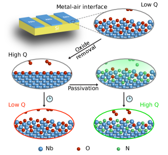
Increasing the coherence time of superconducting qubits while maintaining reasonable gate speeds enables more powerful quantum processorsArute et al. (2019); Jurcevic et al. (2021). The improvement of fabrication techniques plays an important role in this effortOliver and Welander (2013); Murray (2021). The fabrication process of high coherence planar superconducting quantum processors now typically involves two superconducting layers. The first layer makes up the ground plane and all the circuit elements other than the Josephson junctionJosephson (1962); Anderson and Rowell (1963) (JJ) while the second layer defines the JJs. The two-layer process allows optimization of the quality factor of the superconducting capacitor pads independent from the requirements of the double-angle-evaporated aluminum JJ layer. Microwave coplanar waveguide (CPW) resonators have been demonstrated as a robust platform to characterize the microwave loss in superconducting materialsO’Connell et al. (2008a); McRae et al. (2020), and have been instrumental in the continuous improvement of film and device qualityNersisyan et al. (2019); Place et al. (2021). In typical device geometries, less than 1 percent of the electric field energy is stored in the thin dielectric layers at the metal-air (MA), metal-substrate (MS), and substrate air (SA) interfacesWenner et al. (2011); Melville et al. (2020). These dielectric layers may host two-level-system (TLS)Müller, Cole, and Lisenfeld (2019) defects resulting in a high loss tangent O’Connell et al. (2008a); Wenner et al. (2011); Melville et al. (2020) that dominates the single-photon energy loss of state-of-the-art superconducting devices, despite the small participation of these dielectric layers. For Nb resonators, the primary TLS loss comes from the oxide layerSheridan et al. (2021); Proslier et al. (2011) at the MA interface. As the electric field energy stored in a thin dielectric layer at the interface is proportional to its thicknessVerjauw et al. (2021), the removal of the oxide results in lower microwave loss. The removal of the surface oxide layer in Nb CPW resonators has resulted in single-photon internal quality factors up to 5 millionAltoé et al. (2020) and filling factor adjusted two-level-system loss tangents down to . However, the oxide grows back following a Cabrera-MottCabrera and Mott (1949) behavior within several hours, reintroducing TLSs at the MA interfaceVerjauw et al. (2021); Sokhey, Rai, and Lodha (2010) (Fig. 1). As the buffered oxide etch (BOE) used to etch also etches the Al JJWilliams, Gupta, and Wasilik (2003), it is difficult to incorporate Nb resonators with a low density of TLSs at the MA interface into superconducting quantum circuits.
Nitride superconductors such as NbN and TiN are known to only have a thin native surface oxide layer at room temperature and therefore are expected to have fewer TLSs at the MA interfaceZhang et al. (2018). As for the MS interface, recent studiesVissers et al. (2010); Rao et al. (2018); Shearrow et al. (2018); Yost et al. (2020) have shown that high quality TiN (200) films can be deposited directly on Si substrate without a seed layer deposited in a separate process step which reduces the total microwave loss. However, the microwave loss of TiN at the MS interface is still higher than elemental superconductor and work is needed to further improve the quality of the MS interfaceMelville et al. (2020). Resonators with on the order of 1 million have been fabricated using sputtered and atomic-layer-deposited NbN thin filmsCarter et al. (2019); Sheagren et al. (2020), and NbN-based superconducting qubits have reached a relaxation time of 16 Kim et al. (2021). However, the performance of these devices is still below the state of the art necessitating further investigation of NbN films. If a resonator could have the MA interface from a nitride superconductor and the MS interface from an elemental superconductor, then its microwave loss caused by TLS is expected to be extremely low. There have been attempts to deposit a thin TiN film covering Nb to prevent the growth of Berk et al. (2021), but the sidewalls are not covered by TiN and can still oxidize.
Nitrogen dopingGrassellino et al. (2013) is a well-established technique used to create low-loss Nb 3D cavities. By baking the Nb cavity in gas at a temperature above 800 ∘C, a conformal layer of is formed at the MA interface which inhibits the growth of surface oxideSemione et al. (2019). In theory, this method can be adapted to make planar superconducting devices, however the effect of high temperature is not yet well understood. Treatment at high temperature can change the stress and grain size of the deposited metal and allow Nb to diffuse into the Si substrate, which all could potentially affect microwave lossMegrant et al. (2012); Premkumar et al. (2021); Kopas et al. (2020). Baking at high temperature can also introduce dislocation and vacancy defects in the Si substrate, whose effects on microwave loss have not yet been systematically explored.
In this Letter, we demonstrate nitrogen doping of Nb CPW resonators without introducing potentially performance-limiting defects related to high temperature. We utilize a radio frequency (RF) plasma to satisfy the activation energy required for nitrogen doping. We show that a plasma at 300 ∘C for 10 minutes dopes the top 5 nm of the Nb surface with N which suppresses the growth of Nb oxides at the surface. Furthermore, we demonstrate that the passivation remains robust in an ambient air environment for sufficiently long periods of time to incorporate passivated Nb structures into complex, multi-layer quantum processors. Our process can be easily manifested with equipment available in typical industrial and academic facilities.
The films used in this study are fabricated by first cleaning a 2-inch instrinsic Si (111) wafer111Since Nb does not match to the lattice of Si (111) or Si (100), we expect similar results independent of wafer orientation. with resistivity greater than 8000 cm in piranha solution (3:1 mixture of and ) at 120 ∘C for 10 minutes followed by a BOE clean (7:1 mixture of and HF) for 5 minutes. We then load the wafer into an electron-beam evaporation chamber (AJA ATC-ORION-8E) in less than 3 minutes. We evaporate 250 nm of Nb ( purity) at a chamber pressure of Torr and a rate of 2 nm/minMorohashi et al. (2001); Kowsari et al. (2021) at room temperature, resulting in a thickness uniformity better than 2.5% variation. The thickness of the Nb film is confirmed by crystal microbalance and profilometer measurements.
The resonator pattern is defined after we deposit the Nb film and before the passivation steps. We utilize a positive photoresist (MicroChem Shipley S1805) and a 375 nm optical direct-write laser lithography system (Heidelberg DWL 66+) to pattern the film. We etch the patterned film using a mixture of and Ar in an RIE system (Oxford Plasma Lab 100 ICP). Our etching recipe produces a nm deep trench in the Si substrate. We then oxygen plasma ash the samples (100 W, 15 sccm ) for 30 s and finally soak them in MicroChem Remover PG for hours at 70 to remove the remaining resist.
To passivate the samples, we start by performing a BOE clean for 30 minutes to remove all the surface oxide before transferring the wafer into a plasma enhanced chemical vapor deposition (PECVD) chamber (Oxford Instruments Nanofab). The transfer time between removal from the BOE solution and evacuation of the PECVD chamber is kept below 3 minutes. We first let the wafer sit at 300 ∘C for 10 minutes with 1200 sccm flow and a chamber pressure of 1 Torr. We then start a 20 W RF plasma at the same chamber condition for 10 minutes. Lastly, we cool down the chamber to 100 ∘C with 100 sccm of flow over the course of one hour before removing the sample. The passivation process forms a nm thick layer at the exposed Si surface in the trench area. We perform a third BOE clean for 15 s to remove this thin layer.
The PECVD system uses a routine process to remove oxides from the chamber walls. This process introduces residual F in the chamber which reacts with the Nb films. To mitigate contamination from F, we deposit m of on a dummy wafer and the chamber wall immediately before passivating our sample.
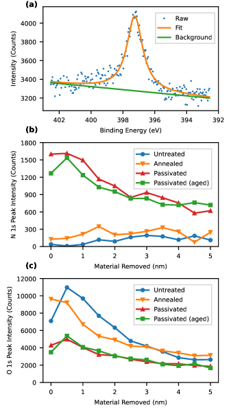
We characterize the surface atomic species of passivated and unpassivated Nb films using X-ray Photoelectron Spectroscopy (XPS). The XPS system (Physical Electronics 5000 VersaProbe II Scanning ESCA Microprobe) uses an Al line source and in-situ Ar ion milling to facilitate analysis of material at depth. Figure 2(a) shows the XPS scan of a passivated Nb film with its top 1 nm removed. The observed peak corresponds to N 1s electrons. We fit the N 1s peak to a psuedo-Voigt function and the background to a linear function. We use the same practice to fit all the N 1s and O 1sRazinkin, Shalaeva, and Kuznetsov (2008) peaks measured in this study.
Figure 2(b) shows the area under the N 1s peak as a function of surface material removed for Nb films with different treatments. The untreated sample and the sample that is simply annealed in at 300 without lighting a plasma do not show a strong N presence. In comparison, plasma passivated Nb film shows a well-defined N peak that persists to a depth of 5 nm, which suggests successful incorporation of N atoms. The intensity of the N peak does not change significantly after we age the passivated Nb sample in an ambient environment for 15 days. In Fig. 2(c), we show that the presence of O in the surface 5 nm is reduced for passivated samples. Similar to N, the O concentration in the plasma passivated sample does not change after being aged in an ambient environment for 15 days.
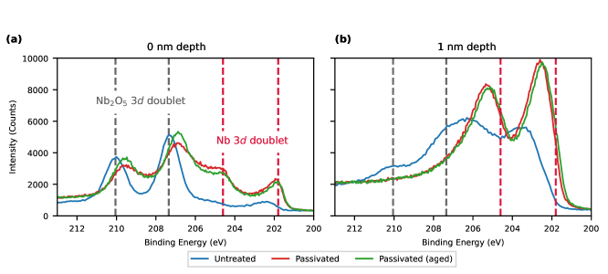
The study of N and O 1s electrons confirms a suppressed oxygen concentration near the surface for passivated samples. We now examine the Nb 3d electrons to investigate the oxides present near the surface of the films. Figure 3 shows the raw XPS spectrum of the different chemical states of the Nb 3d peaks from the same samples shown in Fig. 2. As the stoichiometry of the oxide layer is complexHalbritter (1987) and we have also introduced a nitride with unknown stoichiometry, we expect the spectrum to contain at least 10 individual peaks that overlap with each other. We examine the trend of the energy shift of the dominant peaks from an oxygen-rich high binding energy to lower binding energies which are associated with states that are less oxygen-rich. At zero depth [Fig. 3(a)] we observe clear Nb 3d doublet peaks corresponding to at 207.5 and 210 eV for the unpassivated sample. These two peaks shift to lower energies of 206.8 and 209.3 eV for the passivated films which correspond to a less oxygen-rich Nb oxide state. The un-oxidized Nb 3d doublet peaks are also clearly present at 201.8 and 204.3 eV for the passivated sample. As shown in Fig. 3(b), the unpassivated sample has two dominate peaks at 203.5 and 206.5 eV and a small peak at 210 eV. We associate this to a combination of , , and a large population of . In comparison, the dominant peaks of the passivated sample are at 202.6 and 205.3 eV, which we attribute to a majority of NbO and NbN together with a small amount of Nb. We also observe that the Nb XPS spectrum does not change significantly for the passivated sample after 15 days of aging in an ambient environment. This indicates that the passivated sample does not accumulate significantly more oxide over this period of time.
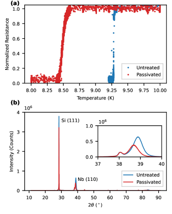
To study the effect of the passivation process on the quality of the Nb films, we measure the direct-current (DC) resistance of the passivated and the untreated films as a function of temperature using a 4-point technique inside a Quantum Design physical property measurement system (PPMS). Both samples are diced from the same Nb film deposited on the same Si (111) wafer allowing us to attribute the change in film properties to the passivation process alone. We extract the residual resistivity ratio (RRR) by taking the ratio between the resistance value at 297 K and 10 K. We find that the untreated sample has a RRR of 4.86, which is similar to our previous result on Si (100)Kowsari et al. (2021). The plasma passivated sample has a reduced RRR value of 2.96. Figure 4(a) shows the resistance near the superconducting transition of both samples. We observe a superconducting critical temperature of K for the untreated sample, and a suppressed of K for the plasma passivated sample with taken from the temperature value when the resistance drops to half of its residual value in the normal state. The suppressed can be explained by assuming that the top passivation layer is disordered and therefore has a much lower than the Nb film. Given the bilayer system we can estimate the thickness of to be about 14.5 nm in agreement with our observation from the XPS data that N atoms extend at least 5 nm into the surface. Cooper (1961); Gubin et al. (2005). We further estimate the zero temperature penetration depth to be 77 nm for the untreated film and 97 nm for the passivated film Tinkham (2004); Gubin et al. (2005); Van Duzer and Turner (1999).
Figure 4(b) shows the X-ray diffraction (XRD) spectrum of both samples measured in a Rigaku MiniFlex system with a Cu source. Although both samples show similar texture, the Nb (110) peak of the passivated sample has about half of the intensity compared to the untreated film. We do not observe any peaks that are associated to , which confirms our assumption that the layer is disordered.
We utilize cryogenic microwave measurements to extract the power-dependent quality factor of CPW resonator structures, and to study the effect of passivation on the TLS-induced loss in the devices. We apply the passivation process to the resonators after the CPW structures are defined with RIE so that the sidewalls of the resonators are also passivated. The resonators are capacitively coupled to a transmission line with coupling quality factor . Hanger-style resonatorsWisbey et al. (2019); Kowsari et al. (2021) with two types of geometries are fabricated. The first geometry has a center strip width of 3 , gap width of 2 , and has a continuous ground plane. This design allows us to clearly observe the effect of TLSs by maximizing capacitive dielectric lossMüller, Cole, and Lisenfeld (2019) and minimizing inductiveSong et al. (2009); de Visser et al. (2012) and radiativeHuang et al. (2021) losses. The second geometry has center strip width of 20 m, gap width of 12 m, and has holes (55 m2 squares) periodically (every 15 m) etched into the ground planeNsanzineza and Plourde (2014). This design minimizes the capacitive loss but is more susceptible to radiative lossHuang et al. (2021) and loss caused by trapped magnetic fluxSong et al. (2009). We use GE varnish to attach each resonator sample to a microstrip-style microwave launch with Pd-coated Cu metallization and Rogers Duroid 6010LM dielectric. We make 3 wirebonds to each port with 1 mil Al-Si bonding wire. The microstrip launch is enclosed inside a Pd-coated Cu sample package. The package is cooled inside a Rainier Model 103 adiabatic demagnetization refrigerator (ADR) down to 50 mK. We add 100 dB of attenuation distributed among different temperature stages to the input lineWisbey et al. (2019). We shield the sample from stray magnetic fields with a high permeability can (Amuneal Cryoperm) surrounding the sample package. The output of the sample passes through one circulator to a high electron mobility transistor (HEMT) amplifier at the 4 K stage. Further amplification is used at room temperature.
A vector network analyzer (VNA) is used to measure the transmission through the sample. The of each resonator is extracted at different average circulating photon numbers ranging from ~1 to ~ using the diameter correction methodKhalil et al. (2012) (DCM). and the high-power internal quality factor are calculated fromMcRae et al. (2020)
| (1) |
where is the Planck constant, is the resonant frequency of the resonator, is the Boltzmann constant, is the temperature of the resonator, and is the critical photon number that differentiates the high and low power regions. When is large, the contribution to microwave loss from saturable TLSs approaches zero, so gives a good estimate of the other sources of loss which mainly result from quasiparticles, trapped magnetic flux, and radiation.
Figure 5(a) shows a comparison of the value among plasma passivated and untreated samples of both designs. Untreated resonators with the 3 m center strip geometry have an average of . This agrees with the result for untreated samples obtained in our previous studyKowsari et al. (2021), which uses the same design but intrinsic Si (100) wafers instead of Si (111). In comparison, the passivated resonators have an average of , which is 4 times lower than the untreated value. Resonators with the 20 m center strip geometry have an average of for untreated samples and of for passivated samples. Figure 5(b) shows the extracted of the same resonators shown in Fig. 5(a). Resonators with the 3 m center strip geometry show an increased compared to untreated devices. We attribute this potentially to a reduced TLS density in the regions of the sample that are too far from the resonators to be effectively saturated at high power and a reduced spin defects residing in the layerSheridan et al. (2021). The values of the resonators with the 20 m center strip geometry are less uniform. We suspect that this could be due to their susceptibility to trapped vortices and radiation to lossy regions inside the package. The values of our resonators are lower compared to other similar studiesAltoé et al. (2020); Megrant et al. (2012), which we attribute to specific details of the sample packageHuang et al. (2021); Matula (1979) and measurement setup.
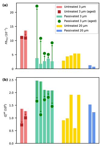
To test the stability of the passivated samples over time, we allow some of the samples to age in an ambient environment for 45 days. Figure 5(a) indicates the change in after this aging duration. We observe negligible change in for the untreated devices, indicating that the oxide had already reached self-limited thickness before the first measurement. The passivated resonators exhibit increased of varying degrees. In particular, two of the five passivated resonators maintained a significantly lower compared to the untreated resonators, validating the stability of the passivated samples. Three of the passivated resonators, however, exhibited a significant increase in , which could be due to additional contamination of the resonators during storage. Visual inspection reveals significant residue and debris in the gap regions of CPWs for the resonators with significantly increased . We attribute this debris to the process of removing, storing, and re-gluing samples into the sample package for the second measurement. In Fig. 5(b) we indicate the change in for the aged devices. For all samples we observe a reduction in after aging.
We extract the filling factor of the MA and MS interface based on a simulation of the cross section of the resonators with 3 center strip using HFSS Q3D extractor. By assuming a dielectric constant (thickness) of 41 (5 nm) for the MA interface and of 4 (2 nm) for the SA interface we obtain a filling factor of for the MA interface and for the SA interface, both of which scale linearly with their thickness. By assuming a loss tangent of for and for Verjauw et al. (2021); Melville et al. (2020), we obtain a total loss of , which agrees with our results of the untreated devices. The microwave loss of the passivated devices agrees with the loss estimated with a 1.3 nm thick layer and a 0.5 nm thick layer. As we do not observe significant change in the O population from the XPS scan, we assume the increase of the microwave loss comes mainly from the increase of thickness from 0.5 nm to 1 nm, which is expected from exposing Si to ambient conditionsMorita et al. (1990).
Our study demonstrates a recipe for passivation of Nb structures with nitrogen plasma which dopes the top 5 nm of the Nb surface with N atoms. These N atoms suppress the O concentration and therefore reduce the amount of TLS defects that induce microwave loss. The N and O populations are stable after 15 days of aging in ambient air according to XPS measurements. Cryogenic microwave measurements confirm that our passivation process reduces the microwave loss of CPW resonators of two different design geometries. Our process removes the stringent time sensitivity associated with the regrowth of and allows for the incorporation of low microwave loss Nb structures into state-of-the-art quantum processors. Our process also creates a platform on which other sources of microwave loss can be further studied. Although and XRD measurements suggest that our process creates a more disordered superconductor, which may increase the susceptibility to losses caused by quasiparticle and magnetic vortices, these mechanisms do not yet dominate the microwave loss. While the side effect of suppressed superconductivity may be reduced by starting with Nb films with large grain size and longer electron mean free path, the suppressed superconductivity may also be useful in producing low loss kinetic-inductance-based sensorsZmuidzinas (2012); Vissers et al. (2013). As Ta also has a superconducting nitrideBreznay et al. (2017) and it is more refractory than Nb, our passivation process may also work in reducing the microwave loss of Ta.
Acknowledgements.
This research is supported by NSF Grant No. PHY-1752844 (CAREER), AFOSR MURI Grant No. FA9550-21-1-0202, DOE grant DE-SC0017987, and the John Templeton Foundation, Grant No. 61835. The authors acknowledge the use of facilities at the Institute of Materials Science and Engineering in Washington University.Data Availability Statement
The data that support the findings of this study are available from the corresponding author upon reasonable request.
References
- Arute et al. (2019) F. Arute, K. Arya, R. Babbush, D. Bacon, J. C. Bardin, R. Barends, R. Biswas, S. Boixo, F. G. S. L. Brandao, D. A. Buell, B. Burkett, Y. Chen, Z. Chen, B. Chiaro, R. Collins, W. Courtney, A. Dunsworth, E. Farhi, B. Foxen, A. Fowler, C. Gidney, M. Giustina, R. Graff, K. Guerin, S. Habegger, M. P. Harrigan, M. J. Hartmann, A. Ho, M. Hoffmann, T. Huang, T. S. Humble, S. V. Isakov, E. Jeffrey, Z. Jiang, D. Kafri, K. Kechedzhi, J. Kelly, P. V. Klimov, S. Knysh, A. Korotkov, F. Kostritsa, D. Landhuis, M. Lindmark, E. Lucero, D. Lyakh, S. Mandrà, J. R. McClean, M. McEwen, A. Megrant, X. Mi, K. Michielsen, M. Mohseni, J. Mutus, O. Naaman, M. Neeley, C. Neill, M. Y. Niu, E. Ostby, A. Petukhov, J. C. Platt, C. Quintana, E. G. Rieffel, P. Roushan, N. C. Rubin, D. Sank, K. J. Satzinger, V. Smelyanskiy, K. J. Sung, M. D. Trevithick, A. Vainsencher, B. Villalonga, T. White, Z. J. Yao, P. Yeh, A. Zalcman, H. Neven, and J. M. Martinis, “Quantum supremacy using a programmable superconducting processor,” Nature 574, 505–510 (2019).
- Jurcevic et al. (2021) P. Jurcevic, A. Javadi-Abhari, L. S. Bishop, I. Lauer, D. F. Bogorin, M. Brink, L. Capelluto, O. Günlük, T. Itoko, N. Kanazawa, A. Kandala, G. A. Keefe, K. Krsulich, W. Landers, E. P. Lewandowski, D. T. McClure, G. Nannicini, A. Narasgond, H. M. Nayfeh, E. Pritchett, M. B. Rothwell, S. Srinivasan, N. Sundaresan, C. Wang, K. X. Wei, C. J. Wood, J.-B. Yau, E. J. Zhang, O. E. Dial, J. M. Chow, and J. M. Gambetta, “Demonstration of quantum volume 64 on a superconducting quantum computing system,” Quantum Science and Technology 6, 025020 (2021).
- Oliver and Welander (2013) W. D. Oliver and P. B. Welander, “Materials in superconducting quantum bits,” MRS Bulletin 38, 816–825 (2013).
- Murray (2021) C. E. Murray, “Material matters in superconducting qubits,” (2021), arXiv:2106.05919 [quant-ph] .
- Josephson (1962) B. Josephson, “Possible new effects in superconductive tunnelling,” Physics Letters 1, 251–253 (1962).
- Anderson and Rowell (1963) P. W. Anderson and J. M. Rowell, “Probable observation of the josephson superconducting tunneling effect,” Phys. Rev. Lett. 10, 230–232 (1963).
- O’Connell et al. (2008a) A. D. O’Connell, M. Ansmann, R. C. Bialczak, M. Hofheinz, N. Katz, E. Lucero, C. McKenney, M. Neeley, H. Wang, E. M. Weig, A. N. Cleland, and J. M. Martinis, “Microwave dielectric loss at single photon energies and millikelvin temperatures,” Applied Physics Letters 92, 112903 (2008a), https://doi.org/10.1063/1.2898887 .
- McRae et al. (2020) C. R. H. McRae, H. Wang, J. Gao, M. R. Vissers, T. Brecht, A. Dunsworth, D. P. Pappas, and J. Mutus, “Materials loss measurements using superconducting microwave resonators,” Review of Scientific Instruments 91, 091101 (2020), https://doi.org/10.1063/5.0017378 .
- Nersisyan et al. (2019) A. Nersisyan, S. Poletto, N. Alidoust, R. Manenti, R. Renzas, C.-V. Bui, K. Vu, T. Whyland, Y. Mohan, E. A. Sete, S. Stanwyck, A. Bestwick, and M. Reagor, “Manufacturing low dissipation superconducting quantum processors,” in 2019 IEEE International Electron Devices Meeting (IEDM) (2019) pp. 31.1.1–31.1.4.
- Place et al. (2021) A. P. M. Place, L. V. H. Rodgers, P. Mundada, B. M. Smitham, M. Fitzpatrick, Z. Leng, A. Premkumar, J. Bryon, A. Vrajitoarea, S. Sussman, G. Cheng, T. Madhavan, H. K. Babla, X. H. Le, Y. Gang, B. Jäck, A. Gyenis, N. Yao, R. J. Cava, N. P. de Leon, and A. A. Houck, “New material platform for superconducting transmon qubits with coherence times exceeding 0.3 milliseconds,” Nature Communications 12, 1779 (2021).
- Wenner et al. (2011) J. Wenner, R. Barends, R. C. Bialczak, Y. Chen, J. Kelly, E. Lucero, M. Mariantoni, A. Megrant, P. J. J. O’Malley, D. Sank, A. Vainsencher, H. Wang, T. C. White, Y. Yin, J. Zhao, A. N. Cleland, and J. M. Martinis, “Surface loss simulations of superconducting coplanar waveguide resonators,” Applied Physics Letters 99, 113513 (2011), https://doi.org/10.1063/1.3637047 .
- Melville et al. (2020) A. Melville, G. Calusine, W. Woods, K. Serniak, E. Golden, B. M. Niedzielski, D. K. Kim, A. Sevi, J. L. Yoder, E. A. Dauler, and W. D. Oliver, “Comparison of dielectric loss in titanium nitride and aluminum superconducting resonators,” Applied Physics Letters 117, 124004 (2020), https://doi.org/10.1063/5.0021950 .
- Müller, Cole, and Lisenfeld (2019) C. Müller, J. H. Cole, and J. Lisenfeld, “Towards understanding two-level-systems in amorphous solids: insights from quantum circuits,” Reports on Progress in Physics 82, 124501 (2019).
- Sheridan et al. (2021) E. Sheridan, T. F. Harrelson, E. Sivonxay, K. A. Persson, M. V. P. Altoé, I. Siddiqi, D. F. Ogletree, D. I. Santiago, and S. M. Griffin, “Microscopic theory of magnetic disorder-induced decoherence in superconducting nb films,” (2021), arXiv:2111.11684 [cond-mat.supr-con] .
- Proslier et al. (2011) T. Proslier, M. Kharitonov, M. Pellin, J. Zasadzinski, and Ciovati, “Evidence of surface paramagnetism in niobium and consequences for the superconducting cavity surface impedance,” IEEE Transactions on Applied Superconductivity 21, 2619–2622 (2011).
- Verjauw et al. (2021) J. Verjauw, A. Potočnik, M. Mongillo, R. Acharya, F. Mohiyaddin, G. Simion, A. Pacco, T. Ivanov, D. Wan, A. Vanleenhove, L. Souriau, J. Jussot, A. Thiam, J. Swerts, X. Piao, S. Couet, M. Heyns, B. Govoreanu, and I. Radu, “Investigation of microwave loss induced by oxide regrowth in high-q niobium resonators,” Phys. Rev. Applied 16, 014018 (2021).
- Altoé et al. (2020) M. V. P. Altoé, A. Banerjee, C. Berk, A. Hajr, A. Schwartzberg, C. Song, M. A. Ghadeer, S. Aloni, M. J. Elowson, J. M. Kreikebaum, E. K. Wong, S. Griffin, S. Rao, A. Weber-Bargioni, A. M. Minor, D. I. Santiago, S. Cabrini, I. Siddiqi, and D. F. Ogletree, “Localization and reduction of superconducting quantum coherent circuit losses,” (2020), arXiv:2012.07604 [quant-ph] .
- Cabrera and Mott (1949) N. Cabrera and N. F. Mott, “Theory of the oxidation of metals,” Reports on Progress in Physics 12, 163–184 (1949).
- Sokhey, Rai, and Lodha (2010) K. Sokhey, S. Rai, and G. Lodha, “Oxidation studies of niobium thin films at room temperature by x-ray reflectivity,” Applied Surface Science 257, 222–226 (2010).
- Williams, Gupta, and Wasilik (2003) K. Williams, K. Gupta, and M. Wasilik, “Etch rates for micromachining processing-part ii,” Journal of Microelectromechanical Systems 12, 761–778 (2003).
- Zhang et al. (2018) L. Zhang, L. You, L. Ying, W. Peng, and Z. Wang, “Characterization of surface oxidation layers on ultrathin nbtin films,” Physica C: Superconductivity and its Applications 545, 1–4 (2018).
- Vissers et al. (2010) M. R. Vissers, J. Gao, D. S. Wisbey, D. A. Hite, C. C. Tsuei, A. D. Corcoles, M. Steffen, and D. P. Pappas, “Low loss superconducting titanium nitride coplanar waveguide resonators,” Applied Physics Letters 97, 232509 (2010), https://doi.org/10.1063/1.3517252 .
- Rao et al. (2018) S. S. P. Rao, C. Hobbs, S. Olson, N. Foroozani, H. Chong, H. Stamper, B. Martinick, D. Ashworth, B. Bunday, M. Malloy, E. Holland, J. Nalaskowski, P. Kearney, T. Ngai, I. Wells, M. Yakimov, S. Oktyabrsky, B. O’Brien, V. Kaushik, K. A. Dunn, K. Beckmann, S. Bennett, M. Rodgers, T. Murray, S. Novak, B. Baker-O’Neal, C. Borst, K. D. Osborn, and M. Liehr, “(invited) materials and processes for superconducting qubits and superconducting electronic circuits on 300mm wafers,” ECS Transactions 85, 151–161 (2018).
- Shearrow et al. (2018) A. Shearrow, G. Koolstra, S. J. Whiteley, N. Earnest, P. S. Barry, F. J. Heremans, D. D. Awschalom, E. Shirokoff, and D. I. Schuster, “Atomic layer deposition of titanium nitride for quantum circuits,” Applied Physics Letters 113, 212601 (2018), https://doi.org/10.1063/1.5053461 .
- Yost et al. (2020) D. R. W. Yost, M. E. Schwartz, J. Mallek, D. Rosenberg, C. Stull, J. L. Yoder, G. Calusine, M. Cook, R. Das, A. L. Day, E. B. Golden, D. K. Kim, A. Melville, B. M. Niedzielski, W. Woods, A. J. Kerman, and W. D. Oliver, “Solid-state qubits integrated with superconducting through-silicon vias,” npj Quantum Information 6, 59 (2020).
- Carter et al. (2019) F. W. Carter, T. Khaire, C. Chang, and V. Novosad, “Low-loss single-photon nbn microwave resonators on si,” Applied Physics Letters 115, 092602 (2019), https://doi.org/10.1063/1.5115276 .
- Sheagren et al. (2020) C. Sheagren, P. Barry, E. Shirokoff, and Q. Y. Tang, “Atomic layer deposition niobium nitride films for high-q resonators,” Journal of Low Temperature Physics 199, 875–882 (2020).
- Kim et al. (2021) S. Kim, H. Terai, T. Yamashita, W. Qiu, T. Fuse, F. Yoshihara, S. Ashhab, K. Inomata, and K. Semba, “Enhanced coherence of all-nitride superconducting qubits epitaxially grown on silicon substrate,” Communications Materials 2, 98 (2021).
- Berk et al. (2021) C. Berk, A. Banerjee, A. HAJR, J. M. Kreikebaum, V. Altoe, D. Santiago, D. F. Ogletree, and I. Siddiqi, “Improvement in superconducting resonator quality factor through surface passivation,” Bulletin of the American Physical Society (2021).
- Grassellino et al. (2013) A. Grassellino, A. Romanenko, D. Sergatskov, O. Melnychuk, Y. Trenikhina, A. Crawford, A. Rowe, M. Wong, T. Khabiboulline, and F. Barkov, “Nitrogen and argon doping of niobium for superconducting radio frequency cavities: a pathway to highly efficient accelerating structures,” Superconductor Science and Technology 26, 102001 (2013).
- Semione et al. (2019) G. D. L. Semione, A. D. Pandey, S. Tober, J. Pfrommer, A. Poulain, J. Drnec, G. Schütz, T. F. Keller, H. Noei, V. Vonk, B. Foster, and A. Stierle, “Niobium near-surface composition during nitrogen infusion relevant for superconducting radio-frequency cavities,” Phys. Rev. Accel. Beams 22, 103102 (2019).
- Megrant et al. (2012) A. Megrant, C. Neill, R. Barends, B. Chiaro, Y. Chen, L. Feigl, J. Kelly, E. Lucero, M. Mariantoni, P. J. J. O’Malley, D. Sank, A. Vainsencher, J. Wenner, T. C. White, Y. Yin, J. Zhao, C. J. Palmstrø m, J. M. Martinis, and A. N. Cleland, “Planar superconducting resonators with internal quality factors above one million,” Applied Physics Letters 100, 113510 (2012), https://doi.org/10.1063/1.3693409 .
- Premkumar et al. (2021) A. Premkumar, C. Weiland, S. Hwang, B. Jäck, A. P. M. Place, I. Waluyo, A. Hunt, V. Bisogni, J. Pelliciari, A. Barbour, M. S. Miller, P. Russo, F. Camino, K. Kisslinger, X. Tong, M. S. Hybertsen, A. A. Houck, and I. Jarrige, “Microscopic relaxation channels in materials for superconducting qubits,” Communications Materials 2, 72 (2021).
- Kopas et al. (2020) C. Kopas, M. K. Murthy, C. Gregory, B. I. Mercado, D. R. Queen, B. Wagner, and N. Newman, “Characterization of the chemical and electrical properties of defects at the niobium-silicon interface,” (2020), arXiv:2011.08359 [cond-mat.mtrl-sci] .
- Note (1) Since Nb does not match to the lattice of Si (111) or Si (100), we expect similar results independent of wafer orientation.
- Morohashi et al. (2001) S. Morohashi, N. Takeda, S. Tsujimura, M. Kawanishi, K. Harada, S. Maekawa, N. Nakayama, and T. Noguchi, “Characteristics of superconducting nb layer fabricated using high-vacuum electron beam evaporation,” Japanese Journal of Applied Physics 40, 576–579 (2001).
- Kowsari et al. (2021) D. Kowsari, K. Zheng, J. T. Monroe, N. J. Thobaben, X. Du, P. M. Harrington, E. A. Henriksen, D. S. Wisbey, and K. W. Murch, “Fabrication and surface treatment of electron-beam evaporated niobium for low-loss coplanar waveguide resonators,” Applied Physics Letters 119, 132601 (2021), https://doi.org/10.1063/5.0066441 .
- Razinkin, Shalaeva, and Kuznetsov (2008) A. V. Razinkin, E. Shalaeva, and M. V. Kuznetsov, “Photoelectron spectroscopy and diffraction of nbox/nb(110) surface,” The Physics of Metals and Metallography 106, 56–66 (2008).
- Halbritter (1987) J. Halbritter, “On the oxidation and on the superconductivity of niobium,” Applied Physics A 43, 1–28 (1987).
- Cooper (1961) L. N. Cooper, “Superconductivity in the neighborhood of metallic contacts,” Phys. Rev. Lett. 6, 689–690 (1961).
- Gubin et al. (2005) A. I. Gubin, K. S. Il’in, S. A. Vitusevich, M. Siegel, and N. Klein, “Dependence of magnetic penetration depth on the thickness of superconducting nb thin films,” Phys. Rev. B 72, 064503 (2005).
- Tinkham (2004) M. Tinkham, Introduction to Superconductivity: Second Edition, Dover Books on Physics (Dover Publications, 2004).
- Van Duzer and Turner (1999) T. Van Duzer and C. Turner, Principles of Superconductive Devices and Circuits, Bibliyografya Ve Indeks (Prentice Hall, 1999).
- Wisbey et al. (2019) D. S. Wisbey, M. R. Vissers, J. Gao, J. S. Kline, M. O. Sandberg, M. P. Weides, M. M. Paquette, S. Karki, J. Brewster, D. Alameri, I. Kuljanishvili, A. N. Caruso, and D. P. Pappas, “Dielectric loss of boron-based dielectrics on niobium resonators,” Journal of Low Temperature Physics 195, 474–486 (2019).
- Song et al. (2009) C. Song, T. W. Heitmann, M. P. DeFeo, K. Yu, R. McDermott, M. Neeley, J. M. Martinis, and B. L. T. Plourde, “Microwave response of vortices in superconducting thin films of re and al,” Phys. Rev. B 79, 174512 (2009).
- de Visser et al. (2012) P. J. de Visser, J. J. A. Baselmans, S. J. C. Yates, P. Diener, A. Endo, and T. M. Klapwijk, “Microwave-induced excess quasiparticles in superconducting resonators measured through correlated conductivity fluctuations,” Applied Physics Letters 100, 162601 (2012), https://doi.org/10.1063/1.4704151 .
- Huang et al. (2021) S. Huang, B. Lienhard, G. Calusine, A. Vepsäläinen, J. Braumüller, D. K. Kim, A. J. Melville, B. M. Niedzielski, J. L. Yoder, B. Kannan, T. P. Orlando, S. Gustavsson, and W. D. Oliver, “Microwave package design for superconducting quantum processors,” PRX Quantum 2, 020306 (2021).
- Nsanzineza and Plourde (2014) I. Nsanzineza and B. L. T. Plourde, “Trapping a single vortex and reducing quasiparticles in a superconducting resonator,” Phys. Rev. Lett. 113, 117002 (2014).
- Khalil et al. (2012) M. S. Khalil, M. J. A. Stoutimore, F. C. Wellstood, and K. D. Osborn, “An analysis method for asymmetric resonator transmission applied to superconducting devices,” Journal of Applied Physics 111, 054510 (2012), https://doi.org/10.1063/1.3692073 .
- Matula (1979) R. A. Matula, “Electrical resistivity of copper, gold, palladium, and silver,” Journal of Physical and Chemical Reference Data 8, 1147–1298 (1979), https://doi.org/10.1063/1.555614 .
- Morita et al. (1990) M. Morita, T. Ohmi, E. Hasegawa, M. Kawakami, and M. Ohwada, “Growth of native oxide on a silicon surface,” Journal of Applied Physics 68, 1272–1281 (1990), https://doi.org/10.1063/1.347181 .
- Zmuidzinas (2012) J. Zmuidzinas, “Superconducting microresonators: Physics and applications,” Annual Review of Condensed Matter Physics 3, 169–214 (2012), https://doi.org/10.1146/annurev-conmatphys-020911-125022 .
- Vissers et al. (2013) M. R. Vissers, J. Gao, M. Sandberg, S. M. Duff, D. S. Wisbey, K. D. Irwin, and D. P. Pappas, “Proximity-coupled ti/tin multilayers for use in kinetic inductance detectors,” Applied Physics Letters 102, 232603 (2013), https://doi.org/10.1063/1.4804286 .
- Breznay et al. (2017) N. P. Breznay, M. Tendulkar, L. Zhang, S.-C. Lee, and A. Kapitulnik, “Superconductor to weak-insulator transitions in disordered tantalum nitride films,” Phys. Rev. B 96, 134522 (2017).
- O’Connell et al. (2008b) A. D. O’Connell, M. Ansmann, R. C. Bialczak, M. Hofheinz, N. Katz, E. Lucero, C. McKenney, M. Neeley, H. Wang, E. M. Weig, A. N. Cleland, and J. M. Martinis, “Microwave dielectric loss at single photon energies and millikelvin temperatures,” Applied Physics Letters 92, 112903 (2008b), https://doi.org/10.1063/1.2898887 .
- Bonin (1996) B. Bonin, “Materials for superconducting cavities,” (1996).