Rb-induced () and () reconstructions on Si(111)-(): A LEED and STM study
Abstract
We present a study of the rubidium adsorption on the Si(111)-() surface and the related Rb-induced reconstructions as a function of deposition temperature and Rb-coverage via scanning tunneling microscopy (STM) and low-energy electron diffraction (LEED). Sample analysis via LEED allowed to observe for the first time a Rb/Si(111)-() reconstruction. The STM image analysis allowed to obtain the first real space characterization of the Rb/Si(111)-() surface. In addition, STM provided a direct and local information on the surface arrangement as well as further insights on the interaction between Si and Rb atoms and on the growth dynamics.
keywords:
Surface Reconstruction, Adsorption, Alkali Metals, LEED, STM+39 3466079369 \abbreviationsSTM,LEED
1 Introduction
Reaction and interaction between metal atoms and semiconductor surfaces are widely studied 1. In particular, the rubidium-silicon system finds application in a large variety of fields. A knowledge of the structural, interfacial, chemical, and electronic properties of the system is thus foremost.
Rubidum, and in general alkali metals (AMs), have simple electronic structure, strong atomic transitions, and inherently high power density due to low ionization energy thus high reactivity. 2. Their reactivity, however, makes the processing, storage and use of AMs in a controlled manner difficult. The growing interest in developing quantum integrated systems sets the focus on miniaturized oxidation-free rubidium cells 3, 4, 5. These cells allow for better scalability and integration in nano-circuits, where commercial getters are not employable. They make use of non-magnetic materials (such as Si), and need to provide low amounts of pure Rb. Among the applications of these miniaturized Rb cells are highly sensitive optical magnetometries, atomic sensors 5, miniaturized atomic clocks 6, quantum computing 7, and controllable combustion 4.
Rubidium on Si has been demonstrated to improve the thermodynamical stability of multilayer Mo/Si mirrors, which are now the most viable technology to construct the optical systems for extreme-ultraviolet lithography 8.
The importance of AMs adsorbed on silicon finds also application in the field of catalysis. It has been reported that AMs can either promote oxidation of Si9, 10 or passivate the silicon surface depending on the alkali-induced silicon surface reconstruction 11, 12. Catalytic oxidation using AMs finds its application in the formation of the SiO2-Si interface. Standard silicon oxidation process requires very high temperatures which are not always compatible with device fabrication processes. The advantage of the AM as catalyst is that it can be removed by a moderate thermal annealing, thus with low power cosumption and the systems results contaminations-free. Certain types of AM-induced reconstructions of the Si surface, such as the () reconstruction, have been reported to passivate the surface against oxidation. This also finds a large variety of applications, for example in solar cells 13.
In the past, overlayers on semiconductor surfaces have attracted great attention for the study of metal-semiconductor interactions and interface formation as well as for metallization processes. Due to their simple electronic structure, AM overlayers on semiconductor surfaces represent simple model systems for the more general case of metal-semiconductor studies 14, 15. Nowadays, the research focus has been set on ordered nanostructures, stimulated by their great potential for next generation devices. To control the nanostructure dimensions, spatial distribution and uniformity, knowledge of the mechanisms for their spontaneous formation is crucial. In particular, one-dimensional (1D) metal atomic chain systems on semiconductor surfaces have attracted substantial attention because of their intriguing electronic properties and potential applications in atomic scale devices 16, 17.
Various self-assembled arrays of metal atomic chains on semiconductors have been observed at submonolayer metal coverages, and a () phase has been frequently observed on the Si(111) surface. This reconstruction is formed by all AM (Li, Na, K, Rb, Cs) 18, 19, 20, 21, 22, 23, 24, 25, 26, 27, 28, 29, 30, monovalent Ag 31, 32, alkaline earth metals (Mg, Ca, Sr, Ba) 33, 34, 35, 36, and rare earth metals (Yb, Sm) 37, 38, 39. Some similarities as well as differences exist in the appearance of the reconstruction induced by various adsorbates and in particular among different AMs. Despite more than two decades of experimental efforts on these surfaces, some issues still need to be solved.
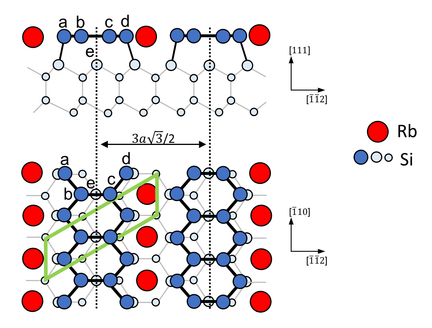
The surface geometry of the () reconstruction has been studied both experimentally and theoretically, and many structural models have been proposed. Among the proposed models, the honeycomb-chain-channel (HCC) 40, 41, 42 is nowadays widely accepted. In the HCC model, shown in Fig. 1, “honeycomb chains” are formed by four inequivalent Si surface atoms. The inner atoms (b, c in Fig. 1), threefold coordinated in a planar configuration via Si double bonds (sp2-like), interact only weakly with the Si atom below, indicated as e in Fig. 1. The resulting -bond is primarily responsible for the stability of the HCC model. The dangling bond on the outer atoms (a, d in Fig. 1), roughly tetrahedrally coordinated, is fully occupied due to the electron donation of the AM and to the electron distribution associated with the Si adatoms and the underlying atom (e in Fig. 1). The AM atoms are fully ionized and sit in a channel formed by neighboring honeycomb chains and form parallel ordered one-dimensional rows in the [] direction.
In agreement with the HCC model, recent experimental work arrived at a consensus coverage of ML for the AM in the () phase, where one monolayer (ML) refers to the Si atomic density in the Si(111)-() surface () 43, 44, 45. STM analysis of the () surface reveals that this phase is imaged as double zig-zag rows of silicon atoms running along the [] direction, separated by a missing row, which accommodates the AMs. The zig-zag rows are spaced by Å, where Å is the Si(111)-() lattice constant 21. A semiconducting character of the () surface has been reported for Li 44, Na 46, 19, and K 28. In addition, passivation against oxidation has been reported for the Na 11 and K /Si(111)-() surface 12. In the case of Cs adsorbed on the Si(111)-(), photoemission spectroscopy and LEED showed that at high Cs coverage the () structure is transformed into a () 30, 23. An AM/Si(111)-() reconstruction has only been reported for Cs so far.
In the particular case of the Rb/Si(111) surface, the experimental evidence of the () reconstruction is limited to diffraction and core level spectroscopy studies. The () reconstruction was observed depositing Rb on a clean Si(111)-() surface at elevated temperatures 18. Moreover, x-ray standing wave studies of samples obtained by RT deposition of Rb reported an increased order of the surface after an annealing at ℃ 47, attributed to the formation of the () phase. No evidence of the () reconstruction was found in these studies after RT deposition, but rather a preferential adsorption of Rb on multiple sites of the () surface was reported 48, 49, 50, 51. The Si 2p core level spectrum of the Rb/Si(111)-() surface was well fitted by one bulk and three surface components 52, consistent with the HCC model 42. The Rb 4p spectrum indicated a single adsorbate site on the () surface, consistent with an alkali coverage of 1/3 ML 52.
In this paper we investigate the adsorption of Rb on the Si(111)-() surface and the related Rb-induced reconstructions. In particular, we analyze their dependence on deposition temperature and Rb-coverage with surface sensitive techniques such as LEED and STM. We report the first real space images of a Rb induced () reconstruction as well as the first observation of a Rb() reconstruction. Finally, we discuss the mechanisms of reconstruction, analyzing the importance of substrate temperature and suggest an explanation for the appearance of the () structure.
2 Experimental
The Si(111) samples were cut from commercial silicon wafers with 500 m thickness. The whole experiment (sample preparation and characterization) has been performed in an ultra-high vacuum (UHV) environment, with a base pressure better than mbar. Clean and well reconstructed Si(111)-() surfaces were prepared in situ by heating the as-cut samples () to 1000℃, after an overnight outgassing at 600℃. This preparation method allows to obtain a Si(111)-() surface characterized by clean, parallel, and fairly regular ( nm large) flat terraces separated by steps nm high. Rb was evaporated from a commercial getter source (SAES Getters Inc.) with a rate of about 0.03 ML/min onto the Si(111)-() surface held either at room temperature or at elevated temperatures ranging from 300 to 400℃. Depositions were performed at constant evaporation rate, monitored with a residual gas analyzer (RGA from SRS), on samples kept at constant temperature. Temperatures were measured with an infrared pyrometer with an uncertainty of ℃. LEED and STM characterization was performed at RT. The scanning tunneling microscope used to perform the experiments is a variable-temperature UHV STM from RHK Technology working at a base pressure of mbar. The tips used to scan the samples are electrochemically etched tungsten tips that were first degassed in situ and then flashed by applying high voltage. All STM images were obtained in constant-current mode.
3 Results and Discussion
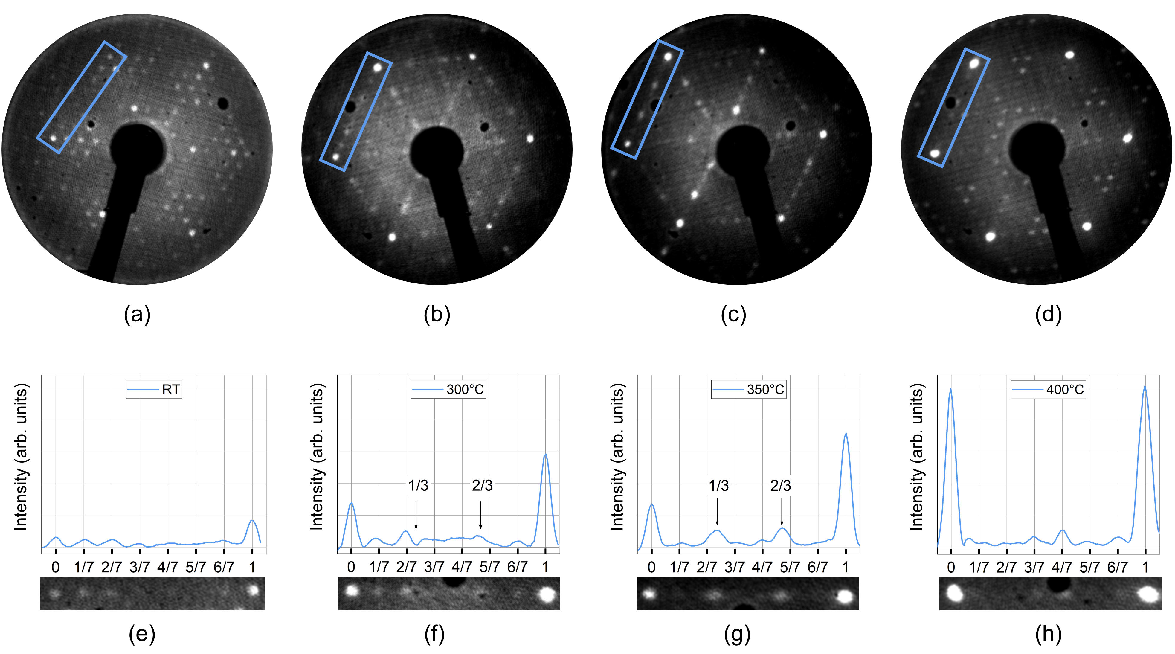
We first report the results on the Rb adsorption behavior as a function of the deposition temperature. Figure 2 shows the LEED patterns of Rb/Si(111) surfaces obtained after 9 minutes of Rb deposition at different temperatures on the clean () surface. When Rb was deposited at RT, the LEED pattern (Fig. 2(a) and 2(e)) retained a () periodicity. However, the surface showed a diffraction pattern with a different intensity distribution compared to the original () pattern observed on the clean silicon sample, underlined by the asymmetry of the () spots otherwise symmetric at this beam energy, as well as highly suppressed spot intensities. When Rb was deposited at 300℃, the LEED pattern (Fig. 2(b) and 2(f)) readily showed the presence of weak and broad spots arranged in a () pattern, superimposed on a sharp pattern with () periodicity. As the deposition temperature was increased, the () pattern became more clear, reaching its maximum intensity with deposition temperatures around 350℃ (see Fig. 2(c) and 2(g)). Around this temperature, the () spots became sharp and clearly distinguishable, while the () spots decreased in intensity. Upon deposition at 400℃ or higher, the LEED pattern showed again a () periodicity (Fig. 2(d) and 2(h)) and no evidence of a () reconstruction. The intensity distribution of this diffraction pattern resembles that of the clean reconstructed silicon sample, in strong contrast to that obtained upon RT deposition.
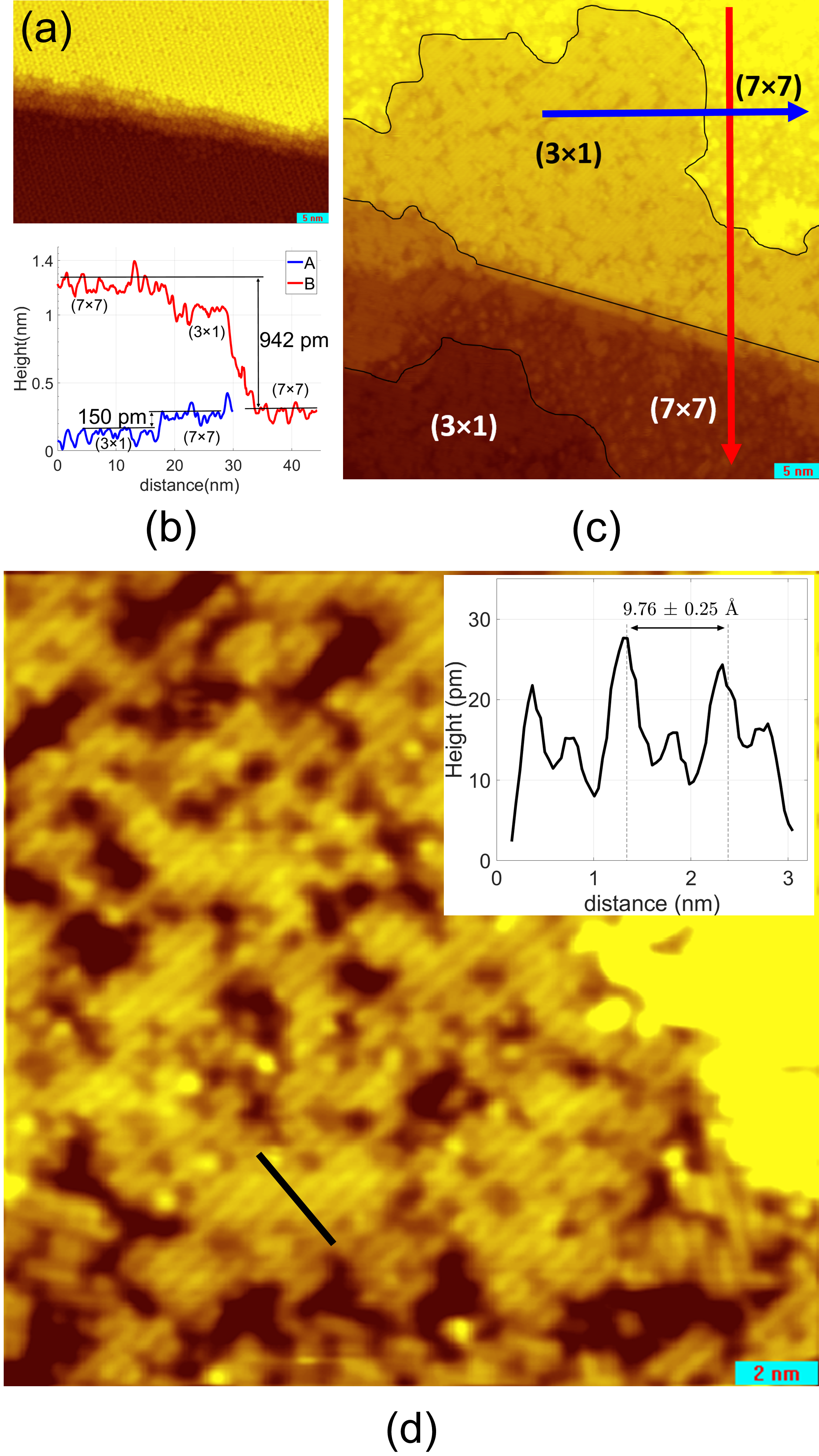
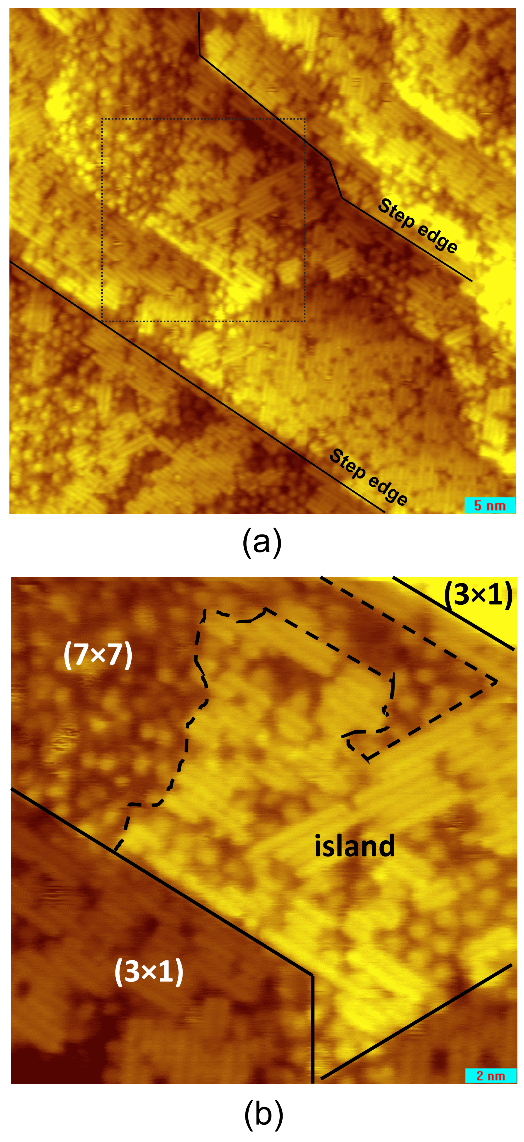
STM analysis of the samples shown in Fig. 2 allowed to account for the amount of () areas. Figure 3(c) shows a large scale STM image of a 9 min Rb-dosed sample (LEED pattern in Fig. 2(c)), in which a change in the terrace geometry can readily be seen compared to the pristine sample (in Fig. 3(a)). The flat () terraces observed in the pristine sample are modified by the Rb adsorption into a two-level system, as highlighted by the blue cross section in Fig. 3(b). The upper level retains a () periodicity, differing from the pristine surface only by the presence of extra atoms adsorbed on the surface. The lower level is occupied by a row structure, characteristic of the () reconstruction. The red cross section in Fig. 3(b) shows that the step height between () levels did not change upon Rb deposition, and its height is an integer multiple of pm, as expected. In addition, the areas characterized by the rows extend inwards from the step edges, as shown in Fig. 3(c). Moreover, the difference in silicon atoms density between the () and the () reconstructions suggests a high silicon mass transport in the transformation from () to (), and thus the presence of excess silicon.
Figure 3(d) shows a zoom into the lower level with the row structure: the filled state STM image shows parallel double rows separated by a “missing row” with a measured distance between the double rows of 9.760.25 Å. Some disorder in the () areas is represented by defects like extra atoms adsorbed on the rows or vacancies within the rows. The geometry of these areas together with the very good agreement with the theoretical distance between the rows 21 makes this the first real space evidence of a Rb-induced () Si(111) reconstruction.
From multiple STM scans of Rb/Si samples after 9 minutes of Rb deposition, the amount of () areas resulted in 0% in the case of RT and 400℃ deposition, and 22% and 65% in the cases of deposition at 300℃ and 350℃, respectively. In addition, in the case of RT deposition, we found a vast amount of Rb adsorbed on the () surface in a disordered fashion, but preferentially on the faulted half of the unit cell (refer to Supplementary Material). In this case, after annealing the Rb/Si sample at 300℃, small patches of () reconstruction on the surface were obtained (refer to Supplementary Material). On the contrary, in the case of Rb deposition at 400℃, only a small number of Rb atoms was found on the silicon surface, not allowing the () to form even after annealing cycles. The aforementioned STM observations prove that at temperatures below 400℃, Rb atoms adsorb on the Si(111) surface, while around and above 400℃ they do not, consistent with the presented LEED evidence. Upon deposition at 300-350℃, Rb atoms arrange to form a surface structure with () periodicity, thus the temperature range for the formation of this reconstruction is at least 50℃. Since we found lowest intensity of the () and highest intensity of the () diffraction spots as well as the highest amount of () surface areas upon deposition at 350℃, we conclude that 350℃ is the optimal temperature for this reconstruction to form, and the following analysis will be centered on samples prepared at this deposition temperature.
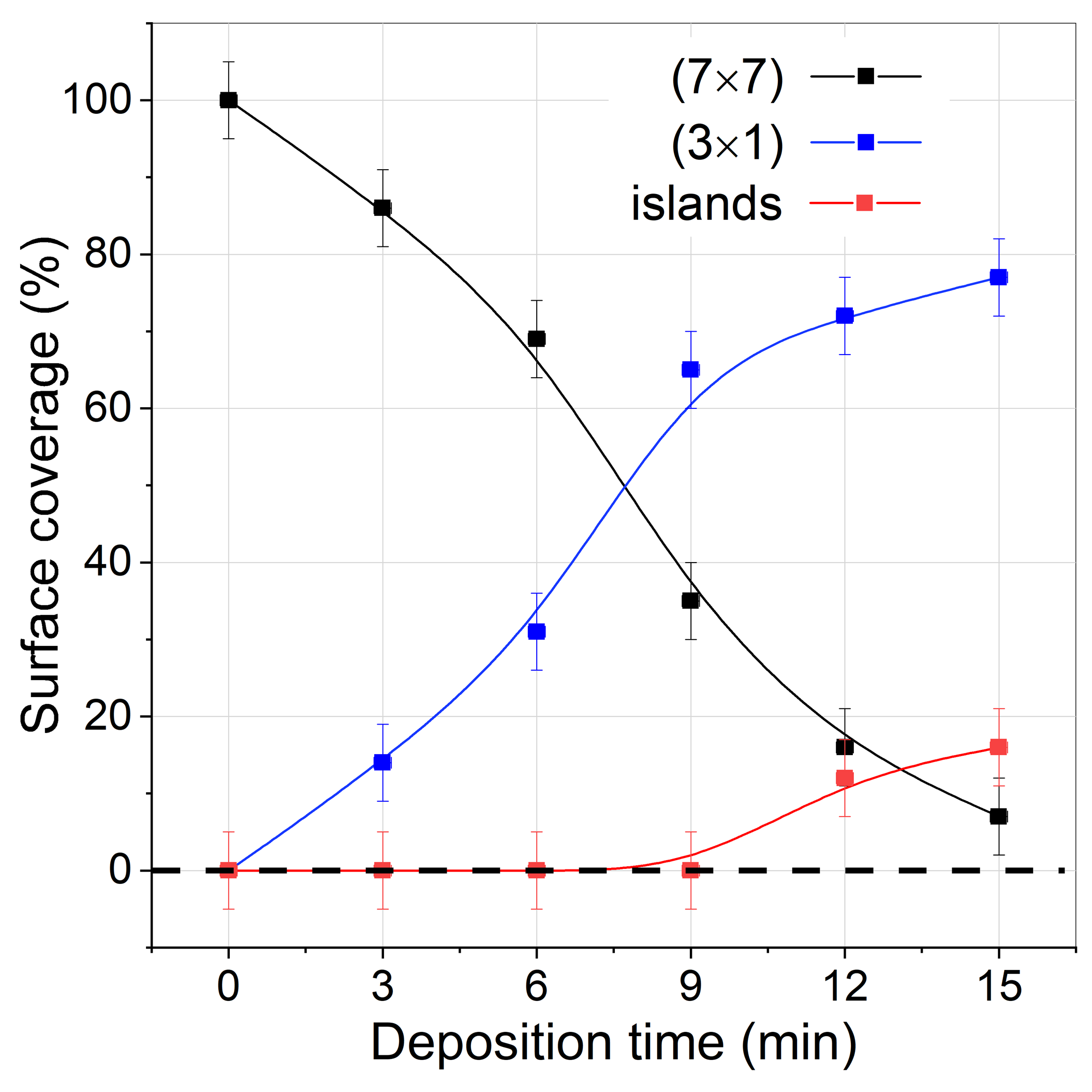
The influence of Rb surface coverage on the reconstruction was studied, as well. Figure 4 reports the results of STM analysis and shows the amount of different reconstructions found on the samples as a function of the Rb deposition time at 350℃. The plot in Fig. 4 clearly shows that, in the studied deposition time range, with increasing deposition time the area retaining a () reconstruction decreases. The presence of a () phase was already revealed after 3 minutes of Rb deposition, both in the LEED patterns and STM images. With deposition time as low as 3 minutes, the terrace system started to transform into a two-level system, with coexistence of () and () phases on the same terrace, as reported in Fig. 3. Up to 9 minutes deposition time, an increase in deposition time led to an increase in the number of () domains as well as an increase in their size, with preferential growth in the [] direction. The two-level system was maintained, as well. After 12 minutes of deposition, we observe a slowdown in the growth of the () areas composing the lower level of the terraces. At the same time, we observe the presence of islands on the upper () level, characterized by a row structure on their surface, as reported in Fig. 5. In addition to these rows, between already formed rows we observe a reordering of atoms towards formation of a row structure, as visible in Fig. 5(b).
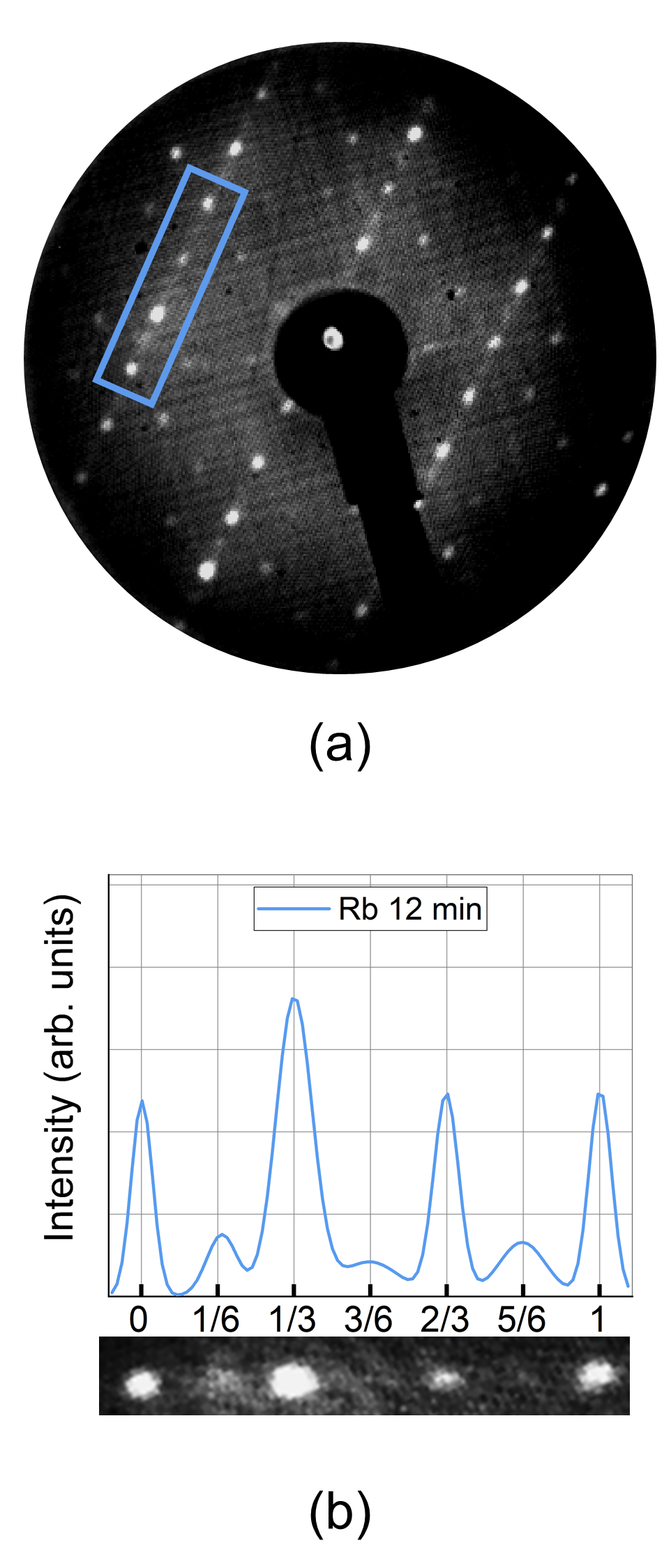
Interestingly, besides the () spots, the LEED patterns obtained upon 12 and 15 min Rb deposition at 350℃ revealed the presence of weak and broad spots arranged in a () pattern (see Fig. 6). The weakness of the () spots suggests that only a small fraction of the surface is arranged with this periodicity. Moreover, the broadening of the () spots indicates the presence of small domains. It is to underline that this is the first time that a Rb() structure is reported.
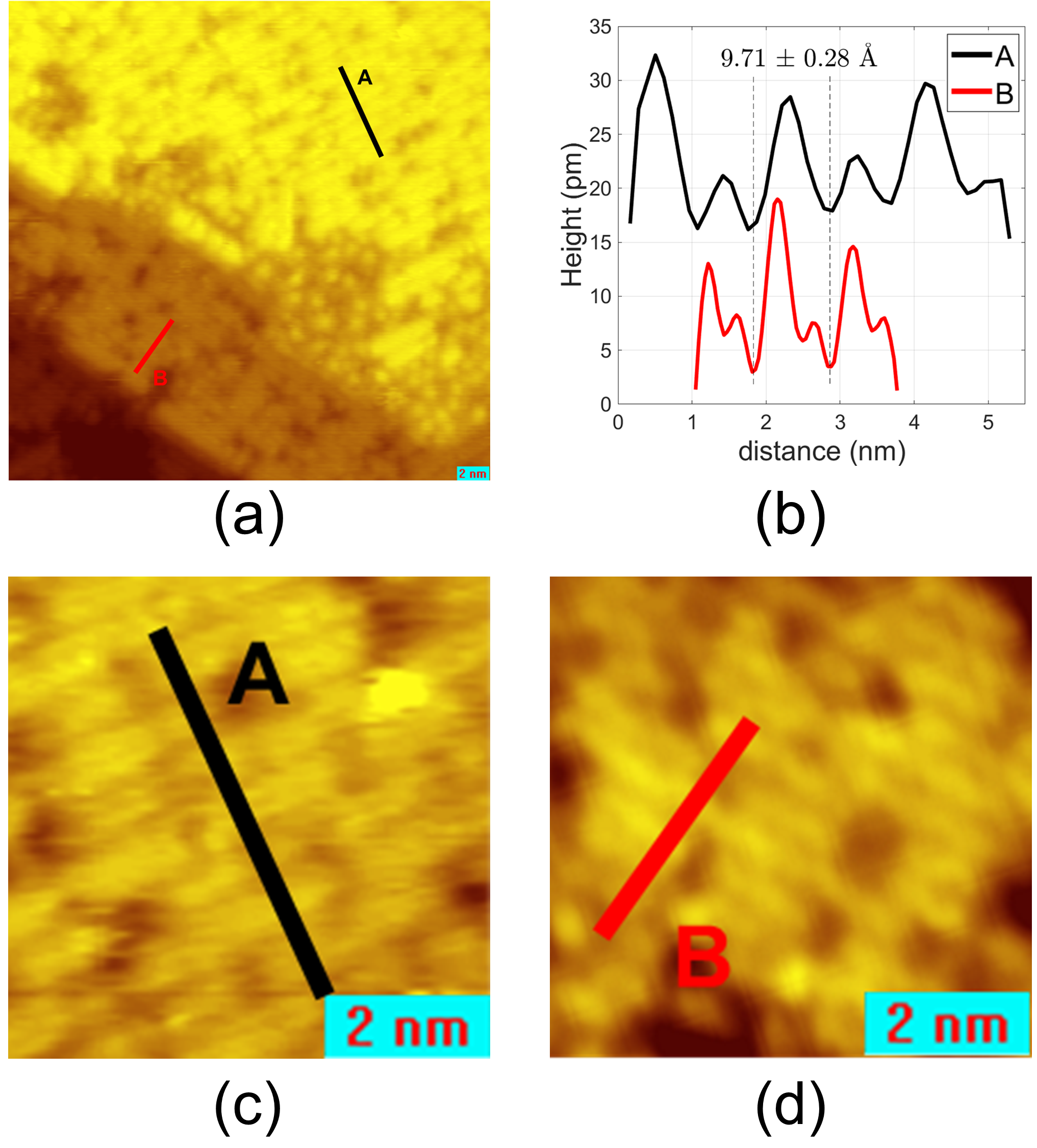
Our STM results show that row structures could be identified both on the lower terrace level and on the islands grown on the upper () terrace level, as highlighted in Fig. 5(b). However, for some of the islands on the () terraces we observe a different height distribution between neighbouring rows (A, black cross section in Fig. 7) when compared to the height distribution of the () areas (B, red cross section in Fig. 7). Despite the fact that single rows could not be resolved in the cross section taken on the island, we note that each peak in (A) corresponds to two neighbouring rows in (B). This suggests that two neighboring rows on the island are seen merged together as a single row. Besides, there is an alternation in the height of these structures in (A), which is markedly different from (B) where each () element is imaged with the same height. Thus, this alternation of height results in a doubled periodicity with respect to the () structure, which means that these atoms are arranged in a () structure.
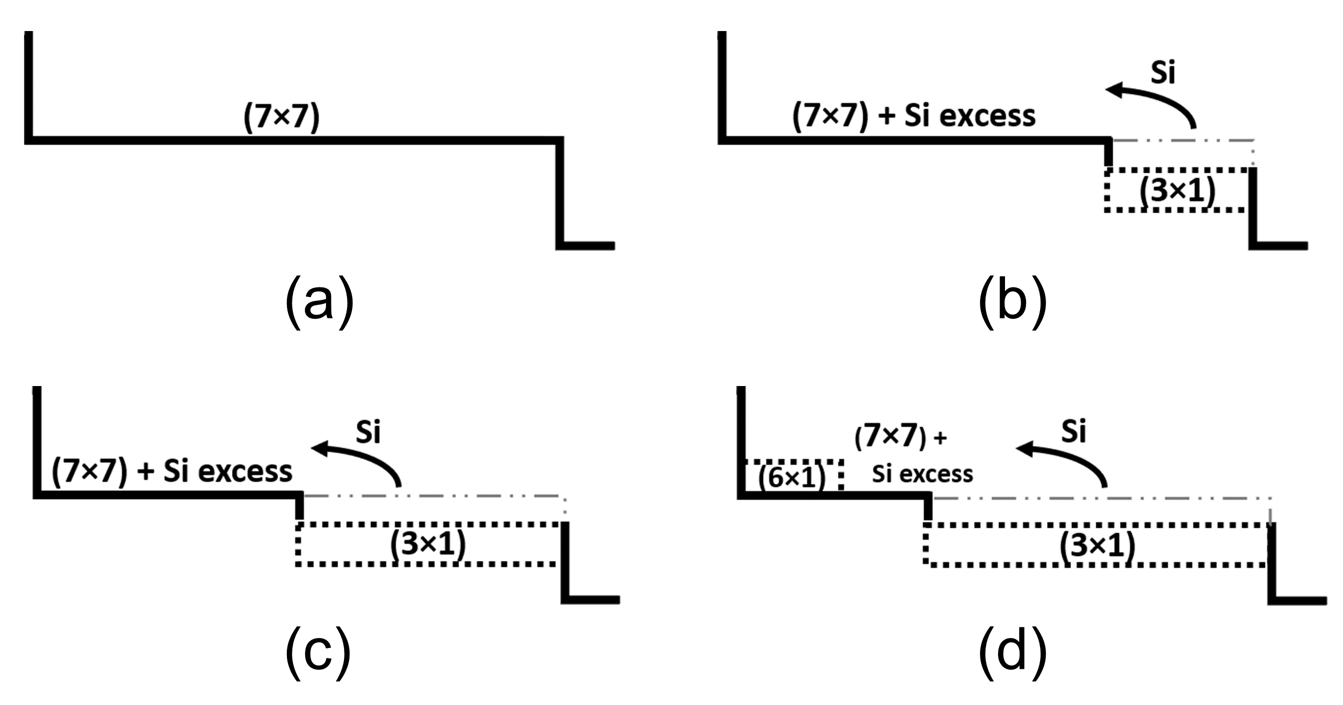
Based on our experimental observations, we suggest for the reconstruction process the following model. A balance between adsorption, desorption, and diffusion processes must be reached in order for the reconstruction processes to happen. Indeed, we observed that the () reconstruction appears after RT deposition only upon annealing, or when the substrate is held at elevated temperature during deposition, in a precise and narrow range of temperatures. Upon deposition at RT, Rb atoms have small diffusion length. Nevertheless, despite the low mobility, the system will try to reach the configuration of lowest energy. What we see is adsorption preferentially on the faulted half of the unit cell. When Rb is deposited at higher temperatures, the thermal energy will promote Rb diffusion on the surface and surface reactivity. If desorption can be neglected, the () conversion process can start. On the other hand, STM shows that at 400℃ and above the desorption process dominates, since little or no Rb atoms were seen adsorbed on the surface, and the reconstruction does not form.
Supposing to be in the optimal temperature conditions for the reconstruction process to happen, then the deposited Rb atoms can migrate on the () surface and react at suitable sites to form the () structure. At the initial stage of formation, we find that suitable sites are at the step edges. These areas are characterized by silicon atoms having higher free energy given by the broken periodicity in the plane, thus an additional dangling bond. Rb reacting with Si atoms will progress towards the energy minimum, which is represented by the () phase. As long as we deposit low-medium amounts of Rb, the Rb-Si reaction will take place predominantly at the step edges and proceed by enlarging row-structure domains inward from the step edge (as sketched in Fig. 8(b) and (c)). Since the () phase is characterized by a smaller Si atom density compared to the () structure ( ML and ML 53), there will be an excess of Si atoms. The Si surplus is ejected onto the surrounding () region (as shown in Fig. 8(b)). This suggests that the excess atoms observed on the () surface are indeed Si atoms.
However, when the excess of silicon becomes important, new favored reaction sites will be formed. Deposited Rb will also react with the excess silicon and form stable reconstructed islands on the () areas, characterized by rows (as sketched in Fig. 8(d)). Besides, the formation of islands as well as the increase in the size of () areas will lead to an important accumulation of compressive strain on the surface.
Thus, the appearance of a () reconstruction for high Rb coverages could be explained in terms of strain release and large Rb atomic size. Strain in the islands would more easily lead to changes in the distance. Conversely, the () reconstruction on the lower terrace levels is more strongly bound to the Si bulk, reconstructed on larger areas, and thus more stable. This might explain why we observe the () only on the islands.
Moreover, the () phase with doubled periodicity could be attributed to the large atomic size of Rb atoms ( pm) and the fact that the Rb nearest neighbor distance (4.84 Å) is larger than the Si(111)-() lattice spacing (3.84 Å) 54. An increased interaction between the two -bonded chains due to the large Rb atoms will cause the two zigzag chain rows to accumulate compressive strain, which can be released by a slight shift between alternating rows to produce the () structure, consistent with the results shown in Fig. 7 and results reported for Cs adsorbed on Si(111) 23, 30.
4 Conclusions
The dependence of temperature and deposition time on Rb induced Si(111)-() reconstructions was studied. We noted that if the deposition temperature is too low (e.g. RT), the () reconstruction will not form. Rb will instead adsorb on the surface preferentially on the faulted half of the () unit cell to minimize the surface energy. On the contrary, if the deposition temperature is too high (above 400℃), Rb atoms will not even stick to the surface, but desorb. Our experimental data suggest 350℃ as the optimal temperature for the formation of the () reconstruction. We show that a range of at least 50℃ wide of suitable temperatures exists for the reconstruction to form. Furthermore, we analyzed the effect of Rb coverage. We obtained the first LEED evidence of a Rb() as well as the first real space characterization of the Rb induced () on the Si(111)-() surface. We suggest a model to explain the growth of these new phases. We analyze the influence of the substrate temperature in terms of diffusion, adsorption and desorption processes and explain the presence of preferential adsorption sites on the surface. Finally, we expose the reasons for the formation of the () as a result of a high amount of deposited Rb in terms of the large Rb atomic size and accumulated strain release from the surface.
Our work allows for a better understanding of Rb interactions with Si. In particular, we discuss in detail how Rb self-assembles into 1D-atomic chains on the Si(111) surface. We provide a detailed recipe to obtain it. The electronic industry is still based on silicon technologies, thus the reduction in dimensionality and the discovery of systems with new properties make studies such as 1D-atomic metal chains on silicon interesting and foremost. Moreover, this Rb-silicon system represents an architecture that might be used to produce in a quite simple way miniaturized Rb cells of extremely pure Rb adsorbed on a non magnetic substrate, and atomically calibrated thanks to the formation of ordered Rb structure on Si(111). In addition, which usage requires small power consumption. Reduction in size, thus integration in nano-circuits, has highlighted the attention on such systems.
STM and LEED study of RT deposition of Rb on the Si(111)-() surface, and after an annealing cycle at 300℃. Rb adsorption behavior and surface induced reconstruction are presented.
References
- chr 2006 Adsorption of Molecules on Metal, Semiconductor and Oxide Surfaces; Landolt-Börnstein: Numerical Data and Functional Relationships in Science and Technology - New Series; Springer-Verlag Berlin Heidelberg, 2006
- Rumble 2020 Rumble, J. In CRC handbook of chemistry and physics: a ready-reference book of chemical and physical data; Ltd, T. . F., Ed.; 2020
- Knapkiewicz 2018 Knapkiewicz, P. Technological Assessment of MEMS Alkali Vapor Cells for Atomic References. Micromachines 2018, 10, 25
- Ruyack et al. 2015 Ruyack, A.; Gund, V.; Camera, K.; Ardanuç, S.; Ober, C.; Lal, A. Alkali Metal Based Micro Combustion Using Graphene Micro-valve Trigger. Journal of Physics: Conference Series 2015, 660, 012033
- Sebbag et al. 2021 Sebbag, Y.; Talker, E.; Naiman, A.; Barash, Y.; Levy, U. Demonstration of an integrated nanophotonic chip-scale alkali vapor magnetometer using inverse design. Light: Science & Applications 2021, 10, 54
- Maurice et al. 2020 Maurice, V.; Newman, Z. L.; Dickerson, S.; Rivers, M.; Hsiao, J.; Greene, P.; Mescher, M.; Kitching, J.; Hummon, M. T.; Johnson, C. Miniaturized optical frequency reference for next-generation portable optical clocks. Opt. Express 2020, 28, 24708–24720
- Saffman 2016 Saffman, M. Quantum computing with atomic qubits and Rydberg interactions: progress and challenges. Journal of Physics B: Atomic, Molecular and Optical Physics 2016, 49, 202001
- Saedi et al. 2020 Saedi, M.; Sfiligoj, C.; Verhoeven, J.; Frenken, J. Effect of rubidium incorporation on the optical properties and intermixing in Mo/Si multilayer mirrors for EUV lithography applications. Applied Surface Science 2020, 507, 144951
- Soukiassian et al. 1986 Soukiassian, P.; Gentle, T.; Bakshi, M.; Hurych, Z. SiO2-Si interface formation by catalytic oxidation using alkali metals and removal of the catalyst species. Journal of Applied Physics 1986, 60, 4339–4341
- Starnberg et al. 1989 Starnberg, H. I.; Soukiassian, P.; Hurych, Z. Alkali-metal-promoted oxidation of the Si(100)2×1 surface: Coverage dependence and nonlocality. Phys. Rev. B 1989, 39, 12775–12782
- Tikhov et al. 1991 Tikhov, M.; Surnev, L.; Kiskinova, M. Na-induced (7×7)-to-(3×1) structural transformation on a Si(111)7×7 surface and the resulting passivation of the surface towards interaction with oxygen. Phys. Rev. B 1991, 44, 3222–3225
- Nelson et al. 1997 Nelson, E.; Kendelewicz, T.; Liu, P.; Pianetta, P. New surface phases for potassium adatoms on cleaved Si(111). Surface Science 1997, 380, 365–376
- Glunz and Feldmann 2018 Glunz, S. W.; Feldmann, F. SiO2 surface passivation layers – a key technology for silicon solar cells. Solar Energy Materials and Solar Cells 2018, 185, 260–269
- Batra 1989 Batra, I. P., Ed. Metallization and Metal-Semiconductor Interfaces; NATO ASI Series; Springer, Boston, MA, 1989; Vol. 195
- Flores 1995 Flores, F. Alkali-atom adsorption on semicondutor surfaces: metallization and Schottky-barrier formation. Surface Review and Letters 1995, 02, 513–537
- Battaglia et al. 2008 Battaglia, C.; Cercellier, H.; Monney, C.; Despont, L.; Garnier, M. G.; Aebi, P. Unveiling new systematics in the self-assembly of atomic chains on Si(111). Journal of Physics: Conference Series 2008, 100, 052078
- Do et al. 2018 Do, E. H.; Kwon, S. G.; Kang, M. H.; Yeom, H. W. Structural and electronic effects of adatoms on metallic atomic chains in Si(111)5 × 2-Au. Scientific Reports 2018, 8, 15537
- Daimon and Ino 1985 Daimon, H.; Ino, S. Study of the Si(111) 77 surface structure by alkali-metal adsorption. Surf. Sci. 1985, 164, 320 – 326
- Jeon et al. 1992 Jeon, D.; Hashizume, T.; Sakurai, T.; Willis, R. F. Structural and electronic properties of ordered single and multiple layers of Na on the Si(111) surface. Phys. Rev. Lett. 1992, 69, 1419–1422
- Fan and Ignatiev 1990 Fan, W. C.; Ignatiev, A. Metal-adsorbate-induced Si(111)-(1×3) reconstruction. Phys. Rev. B 1990, 41, 3592–3595
- Wan et al. 1992 Wan, K. J.; Lin, X. F.; Nogami, J. Comparison of the 3×1 reconstructions of the Si(111) surface induced by Li and Ag. Phys. Rev. B 1992, 46, 13635–13638
- Paggel et al. 1993 Paggel, J. J.; Haak, H.; Theis, W.; Horn, K. Na adsorption on Si(111)-7×7 studied by scanning tunneling microscopy and photoemission. J. Vac. Sci. Technol. B 1993, 11, 1439–1443
- An et al. 1994 An, K.-S.; Yeo, H.-W.; Lee, K.-W.; Park, R.-J.; Kim, J.-S.; Park, C.-Y.; Lee, S.-B. Reconstruction of a Cs-adsorbed Si(111) 77 Surface. J. Korean Phys. Soc. 1994, 27, 111–113
- Hashizume et al. 1991 Hashizume, T.; Motai, K.; Hasegawa, Y.; Sumita, I.; Tanaka, H.; Amano, S.; Hyodo, S.; Sakurai, T. Alkali metal adsorption on the Si(111) surface. J. Vac. Sci. Technol. B 1991, 9, 745–747
- Bakhtizin et al. 1995 Bakhtizin, R. Z.; Park, C.; Hashizume, T.; Sakurai, T. Scanning tunneling microscopy study of the (3 × 1) reconstruction induced by Li adsorption on the Si(111) surface. Appl. Surf. Sci. 1995, 87-88, 347 – 352
- Jeon et al. 1994 Jeon, D.; Hashizume, T.; Sakurai, T. Scanning tunneling microscopy of alkali metal-induced structures on the Si(111) surface. J. Vac. Sci. Technol. B 1994, 12, 2044–2048
- Okuda et al. 1994 Okuda, T.; Shigeoka, H.; Daimon, H.; Suga, S.; Kinoshita, T.; Kakizaki, A. Surface and bulk core level shifts of the Si(111) 3 1-Na and Si(111) -Na surfaces. Surf. Sci. 1994, 321, 105 – 110
- Sakamoto et al. 1994 Sakamoto, K.; Okuda, T.; Nishimoto, H.; Daimon, H.; Suga, S.; Kinoshita, T.; Kakizaki, A. Photoemission study of the Si(111)3×1-K surface. Phys. Rev. B 1994, 50, 1725–1732
- Paggel et al. 1995 Paggel, J. J.; Neuhold, G.; Haak, H.; Horn, K. Scanning-tunneling-microscopy and photoemission study of an alkali-metal-induced structural phase transition: Si(111)-(7×7) into Si(111)-Na(3×1). Phys. Rev. B 1995, 52, 5813–5823
- Park et al. 1995 Park, C.-Y.; An, K.-S.; Kim, J.-S.; Park, R.-J.; Chung, J.; Kinoshita, T.; Kakizaki, A.; Ishii, T. Photoemission study of the Si(111)61-Cs surface. Phys. Rev. B 1995, 52, 8198–8202
- Sakamoto et al. 2001 Sakamoto, K.; Ashima, H.; Zhang, H. M.; Uhrberg, R. I. G. Identification of the basic structure of the Ag/Si(111)- surface: Observation of a low-temperature phase. Phys. Rev. B 2001, 65, 045305
- Gurnett et al. 2002 Gurnett, M.; Gustafsson, J. B.; Magnusson, K. O.; Widstrand, S. M.; Johansson, L. S. O. Angle-resolved photoemission study of the single-domain surface. Phys. Rev. B 2002, 66, 161101
- Quinn and Jona 1991 Quinn, J.; Jona, F. New results on the reaction of Si111 with Mg. Surf. Sci. Lett. 1991, 249, L307 – L311
- Sekiguchi et al. 2001 Sekiguchi, T.; Shimokoshi, F.; Nagao, T.; Hasegawa, S. A series of Ca-induced reconstructions on Si(111) surface. Surf. Sci. 2001, 493, 148 – 156
- Saranin et al. 2000 Saranin, A.; Lifshits, V.; Ignatovich, K.; Bethge, H.; Kayser, R.; Goldbach, H.; Klust, A.; Wollschläger, J.; Henzler, M. Restructuring process of the Si(111) surface upon Ca deposition. Surf. Sci. 2000, 448, 87 – 92
- Weitering 1996 Weitering, H. New barium-induced surface reconstructions on Si(111). Surf. Sci. 1996, 355, L271 – L277
- Wigren et al. 1993 Wigren, C.; Andersen, J. N.; Nyholm, R.; Göthelid, M.; Hammar, M.; Törnevik, C.; Karlsson, U. O. Sm- and Yb-induced reconstructions of the Si(111) surface. Phys. Rev. B 1993, 48, 11014–11019
- Wigren et al. 1993 Wigren, C.; Andersen, J. N.; Nyholm, R.; Karlsson, U. O.; Nogami, J.; Baski, A. A.; Quate, C. F. Adsorption-site determination of ordered Yb on Si(111) surfaces. Phys. Rev. B 1993, 47, 9663–9668
- Eames et al. 2007 Eames, C.; Probert, M. I. J.; Tear, S. P. Quantitative LEED and ab initio study of the surface structure and the missing half-order spots in the diffraction pattern. Phys. Rev. B 2007, 75, 205420
- Collazo-Davila et al. 1998 Collazo-Davila, C.; Grozea, D.; Marks, L. D. Determination and Refinement of the Surface Structure. Phys. Rev. Lett. 1998, 80, 1678–1681
- Lottermoser et al. 1998 Lottermoser, L.; Landemark, E.; Smilgies, D.-M.; Nielsen, M.; Feidenhans’l, R.; Falkenberg, G.; Johnson, R. L.; Gierer, M.; Seitsonen, A. P.; Kleine, H.; Bludau, H.; Over, H.; Kim, S. K.; Jona, F. New Bonding Configuration on Si(111) and Ge(111) Surfaces Induced by the Adsorption of Alkali Metals. Phys. Rev. Lett. 1998, 80, 3980–3983
- Erwin and Weitering 1998 Erwin, S. C.; Weitering, H. H. Theory of the “Honeycomb Chain-Channel” Reconstruction of - . Phys. Rev. Lett. 1998, 81, 2296–2299
- Saranin et al. 1998 Saranin, A. A.; Zotov, A. V.; Ryzhkov, S. V.; Tsukanov, D. A.; Lifshits, V. G.; Ryu, J.-T.; Kubo, O.; Tani, H.; Harada, T.; Katayama, M.; Oura, K. Scanning tunneling microscopy of the to transformation induced on the Si(111) surface by Na adsorption. Phys. Rev. B 1998, 58, 7059–7063
- Weitering et al. 1996 Weitering, H. H.; Shi, X.; Erwin, S. C. Band dispersions of the -bonded-chain reconstruction of Si(111)3×1-Li: A critical evaluation of theory and experiment. Phys. Rev. B 1996, 54, 10585–10592
- Jin et al. 2001 Jin, K.-J.; Sanders, B. C.; Pan, S.-H.; Yang, G.-Z. Row structure in metal-induced Si(111) surface reconstructions. Surface and Interface Analysis 2001, 32, 166–170
- Okuda et al. 1997 Okuda, T.; Sakamoto, K.; Nishimoto, H.; Daimon, H.; Suga, S.; Kinoshita, T.; Kakizaki, A. Angle-resolved photoelectron spectroscopy of the Si(111)3×1-Na surface. Phys. Rev. B 1997, 55, 6762–6765
- Eteläniemi et al. 1993 Eteläniemi, V.; Michel, E. G.; Materlik, G. X-ray standing-wave study of alkali-metal/Si(111)77 interfaces. Phys. Rev. B 1993, 48, 12023–12031
- Lagomarsino et al. 1992 Lagomarsino, S.; Scarinci, F.; Castrucci, P.; Giannini, C.; Fontes, E.; Patel, J. R. Structural study of the Si alkali-metal interface with x-ray standing waves. Phys. Rev. B 1992, 46, 13631–13634
- Castrucci et al. 1993 Castrucci, P.; Lagomarsino, S.; Scarinci, F.; Giannini, C. Multisite occupancy at the alkali/silicon (111) interface studied with XSW. J. Phys. D: Appl. Phys 1993, 26, A192–A196
- Rodrigues 1993 Rodrigues, D. Alkali-metal adsorption on Si(111) surfaces: a comparative study of the bonding nature for Li, Na, K and Rb. J. Phys.: Condens. Matter 1993, 5, A123–A126
- Clotet et al. 1995 Clotet, A.; Ricart, J. M.; Rubio, J.; Illas, F. Nature of bonding of alkali metals ti Si(111). Phys. Rev. B 1995, 51, 1581–1592
- Okuda et al. 1997 Okuda, T.; Daimon, H.; Suga, S.; Tezuka, Y.; Ino, S. Surface electronic structure of ordered alkali- and noble metal-overlayers on Si(111). Appl. Surf. Sci. 1997, 121-122, 89–97
- Saranin et al. 1998 Saranin, A. A.; Zotov, A. V.; Lifshits, V. G.; Ryu, J.-T.; Kubo, O.; Tani, H.; Harada, T.; Katayama, M.; Oura, K. Reexamination of the reconstruction on the basis of Si atom density and unit cluster determination. Phys. Rev. B 1998, 58, 3545–3548
- Hermann 2011 Hermann, K. Crystallography and Surface Structure; John Wiley & Sons Ltd, 2011; Chapter Appendix E, pp 265–266