Beyond Lambertian light trapping for large-area silicon solar cells: fabrication methods
Abstract
Light trapping photonic crystal (PhC) patterns on the surface of Si solar cells provides a novel opportunity to approach the theoretical efficiency limit of 32.3%, for light-to-electrical power conversion with a single junction cell. This is beyond the efficiency limit implied by the Lambertian limit of ray trapping 29%. The interference and slow light effects are harnessed for collecting light even at the long wavelengths near the Si band-gap. We compare two different methods for surface patterning, that can be extended to large area surface patterning: 1) laser direct write and 2) step-&-repeat reduction projection lithography. Large area throughput limitations of these methods are compared with the established electron beam lithography (EBL) route, which is conventionally utilised but much slower than the presented methods. Spectral characterisation of the PhC light trapping is compared for samples fabricated by different methods. Reflectance of Si etched via laser patterned mask was at visible wavelengths and was comparable with Si patterned via EBL made mask. The later pattern showed a stronger absorbance than the Lambertian limit. (M.-L. Hsieh et al., Sci. Rep. 10, 11857 (2020)).
I Introduction
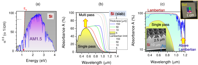
Solar installations will soon provide 1 TW of power from TW we consume per year now with an annual uptake of solar increasing by [1, 2]. Around the world, the most common type of photovoltaic installation is the venerable silicon solar cell, which has a typical efficiency of [3]. The efficiency of a hypothetical Si solar cell which perfectly absorbs all sunlight in the 300-1200 nm wavelength range and has no bulk or surface recombination losses is defined by the Shockley–Queisser limit of at room temperature [4]. Real solar cells cannot absorb all such sunlight and even the purest silicon suffers from Auger recombination losses. The ray optics picture of light trapping suggests that solar absorption cannot exceed the so-called Lambertian limit. To go beyond the ray optics limit, a wave-interference-based light trapping solution needs to be engineered [5] (Figure 1(a) and 1(b)). The Lambertian limit is given by the maximum of optical path enhancement in a weakly absorbing and optically thick medium , here is the real part of the complex refractive index . The Lambertian limit of absorbance , with being the absorption coefficient at the wavelength and is the thickness of the cell.
It was recently shown that photonic crystals (PhC) made via surface texturing and targeting the 0.9-1.2 m spectral range is the key to surpassing the light trapping Lambertian limit [6]. A thin 10-m device layer of silicon-on-insulator (SOI) was textured by inverted pyramid or tee-pee PhC structures of lattice constant m or 1.2 m, respectively (Figure 1(c)). The demonstrated light trapping results propels the solar-to-electrical energy conversion to [6]. This performance was predicted theoretically and it is attainable with only -m-thick Si [7], which is very attractive for applications of lightweight flexible solar cells that can be coated on a variety of surfaces and have higher power conversion efficiency than present-day solar panels [8]. Flexible multi-junction solar cells are sought after in the automotive industry where high efficiency is required and there is a limitation of available surface area [9].
Interdigitated back contacts (IBC) solar cells are currently the most efficient, breaking through the long-held 25% efficiency and performing above , closing the gap to the Lambertian limit [11, 12]. The final selection of an optimised surface texturing will be made upon full characterisation of the material’s response [11]. Recently, it was shown that surface recombination velocity (SRV) in IBC Si solar cells can reach 10 cm/s after processing [11]. Surface nano-texturing by nanoscale needles - black-Si - can be utilised for anti-reflective function [13]. However, when black-Si was applied to Si solar cells, the best efficiency of only was achieved [14]. Also, a prohibitively high SRV value of cm/s was estimated on etched surfaces of black-Si [15]. It is not expected that the light-trapping methods based on ray-optics, when applied to conventional Si solar cell architecture, allows it to reach efficiencies beyond 28% [5]. The optimised IBC solar cells of 15 m thickness with PhC light trapping should perform at % efficiency even when SRV is as high as 100 cm/s [5]. The importance of good surface passivisation for Si solar cells [16] was demonstrated recently by record performing (26% efficient) both-side-contacted [17] and SiC-based highly transparent passivating contacts on 24% efficent cells [18].
In this study, we compare two different methods to define and fabricate PhC light trapping on Si using etch mask patterning by: 1) direct laser writing by ablation and 2) stepper photo-lithography. For comparison, electron beam lithography (EBL) (as in ref. [6]) was also used. Process development and challenges are compared towards the goals of large area cm2 fabrication of light trapping textures on Si, from the perspective of area up-scaling, throughput and technological bottlenecks.
II Results
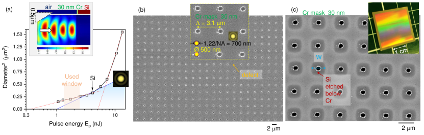
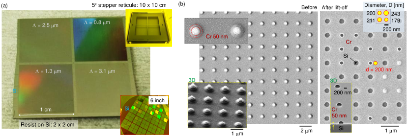
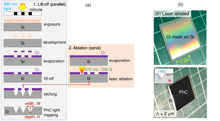
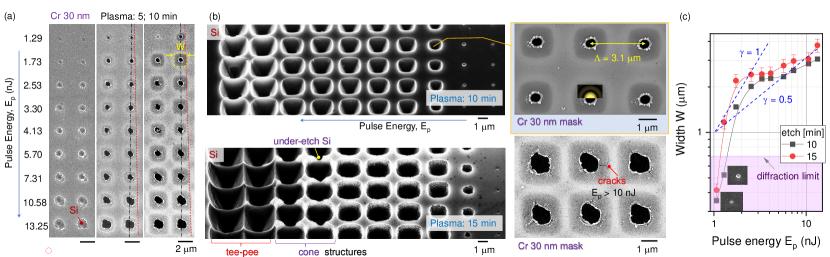
Laser ablation of etch mask. The simplest method to define a mask for plasma-based reactive ion etching (RIE) and/or wet etch of Si is direct laser ablation of sub-1 m diameter holes in a film (Figure 2). Chromium, which is known for good adhesion to many different surfaces and is compatible with plasma and wet etch protocols of Si, was e-beam evaporated on Si and used for the mask. The refractive index of Si and Cr at nm, the wavelength used for ablation, is and , respectively. The reflectance of Si and Cr (see Section V) are and , respectively (note, for bulk samples). A film of chromium nm thickness transmits only of pulse, where . The absorbed component of the energy is utilised for ablation. This shows that energy is deposited almost exclusively into the Cr film, even if it is nano-thin (inset in Figure 2(a)). For focusing with a numerical aperture objective lens, the focal spot radius was nm, the average fluence per pulse J/cm2 for nJ and average pulse irradiance (intensity) TW/cm2 for fs pulse duration. This coincides with the ablation threshold of Si J/cm2 [19].
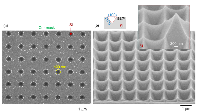
The diameter of the ablated hole is defined by the pulse energy density (fluence), which for the Gaussian beam follows the dependence plotted in Figure 2(a), here is the radial coordinate of Gaussian fluence (intensity) distribution, is the waist of the beam and is the amplitude of fluence [20]. The linearised equation for the used focusing is plotted by a solid line; see the thumbnail-inset of the Airy pattern where the first minimum is used as an approximation for the waist of the beam. For a bulk sample, this dependence would determine the threshold of ablation at the x-axis intercept. For the nano-film used in this study, two distinct regions with different slopes and thresholds were observed. Changes of the slope occurred when an ablation of Si become evident in the ablation crater (see the arrow marker Si in Figure 2(a)). Different slopes reflect different formation mechanisms of the ablation hole. The smaller threshold of J/cm2 is consistent with Cr ablation since the most of pulse energy is deposited in Cr as calculated above. The larger threshold for the faster growing part of the dependence reflects thermal diffusion influence in the formation of larger ablation craters. Detailed mechanisms of the formation of the ablated opening in the mask is beyond the scope of the current study. The pulse energy nJ (on the sample) was chosen for reproducible ablation of m holes; pulse-to-pulse stability of laser was . They were slightly smaller than the diameter of the focal spot as defined by the first minimum of the Airy pattern; see inset in Figure 2(b). The ring around the rim of ablated crater facilitated long plasma etch times with no mechanical support from under etched Si. The ring is likely made out of a nano-alloy of Si and Cr which was not etched during the standard Cr-etch (see Supplementary Figure S5 for discussion). With the established mask fabrication conditions, it was possible to fabricate large areas ( cm2 inset in Figure 2(c)) within several hours (up to 10 h dependent on pattern density). The 20-30 nm Cr film is partly transparent in SEM observation and was used to determine the required etch time to obtain the narrowest ridges between the etched tee-pees (inverted pyramids); here the period . After plasma or wet KOH etch of PhC pattern on Si, Cr mask was removed with a chrome etch solution.
A detailed summary of the width evolution during etch time for different diameter holes in Cr-mask ablated by correspondingly different single laser pulses of energy are presented in Figure S2. We took advantage of the semi-transparent nature of the 30 nm Cr mask in the SEM to explore structure changes during etching. For pulse energies nJ, Si:Cr alloying took place instead of ablation (see Supplement for details). This was evidenced during etching when those regions acted as a mask rather than a hole. When pulse energies exceeded nJ, less regular ablation craters were observed, which showed crack development in Cr mask after long min etching times. Under etch of Si via ablated hole in the Cr mask was slow and followed slope with (Figure S2). Silicon under etch below the Cr-mask showed an anisotropy guided by the crystallinity of the Si plane, which is most pronounced in the case of wet etching in KOH when inverted pyramids are formed. This anisotropy was responsible for the formation of under etch which was slowest in the diagonal direction of tee-pees and caused formation of protruding corners (marked as cones in Figure S2(b)). Interestingly, the metal masks are known to facilitate under etch even for amorphous substrates [21] and could be used for more intricate control of the pattern. Once neighbouring tee-pee pits separated by m approached each other, the narrow ridges were formed (Figure S2(b)). For longer etching, PhC patterns became deeper, however, the depth and width of individual tee-pees did not change. This condition was further exploited for the narrowest ridges . Tens of minutes was enough to etch PhC structures. We used a slightly thicker Cr film of 50 nm for longer plasma etch to ensure complete under etch and the narrowest ridges in earlier studies of phenomena presented (Figure 3). The under etch is illustrated by a pyramidal tip which formed in the place of missing ablation hole in the mask (as shown in Figure 2(b)). Patterns of tee-pee PhC etched in the case of under etch showed similarity to those obtained by anisotropic wet etchning in KOH. Wet etching through ablated holes of m was taking hours in 30% KOH at C. Plasma etching took only tens of minutes for similar PhC patterns.
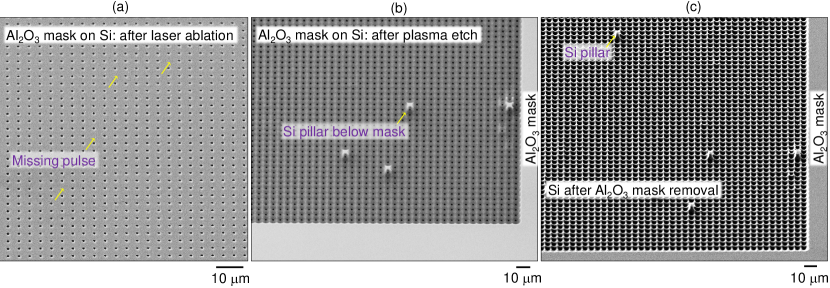
A dielectric alumina \ceAl2O3 film of 20-30 nm, which serves as a part of an antireflection and passivation coating of IBC cells [11], can be used for fabrication of PhC patterns on Si using the same laser ablation method demonstrated for Cr at slightly larger laser pulse energy (Fig. S3). A simpler solvent-based ultrasonic bath removal of the alumina mask after plasma etching is another advantage of this processing, which avoids metal-ion wet chemistry.
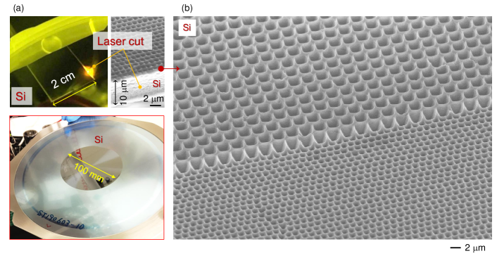
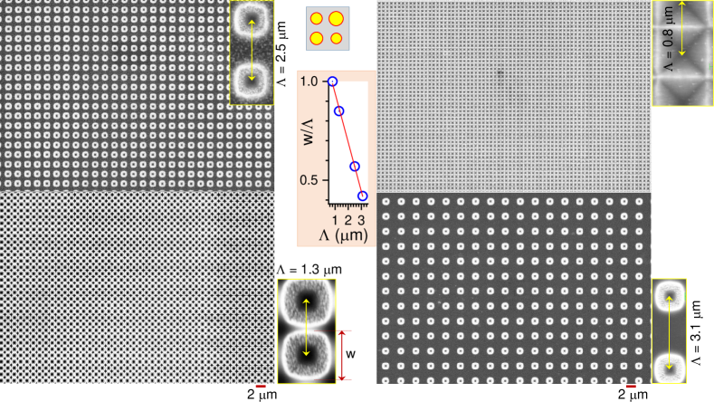
Finally, to show capability to process thin Si wafers of m thickness which is the target for a PhC enhanced light trapping, the same laser processing of Cr mask and plasma etching was carried out (Figure 4). Si cm2 samples were laser cut from the micro-thin wafer using the same fs-laser with focusing objective with (Figure 4(a)). For handling, the thin Si film was attached to a 4-inch sapphire wafer using resist, AZ1518. The resist is spin coated to be m on the sapphire wafer which acts as an initial carrier substrate, with the resist acting as an intermediary layer between the thin Si and the sapphire. This can be subsequently handled by laser cutting the Si to a desired size (Figure 4(a)) and later put into a solution with developer for transfer to a new carrier substrate in the same way as previously mentioned for PhC patterning. It is important to have a very uniform resist film, to keep the attached Si as flat as possible making fabrication conditions ideal. Strong under etch below the Cr mask defined smaller ridges for smaller period for the PhC as compared with larger (Figure 4(b)). The under etch is manifested by different heights of the PhC patterns with different periods m and 1.5 m which were laser ablated on Cr mask side-by-side.
Stepper patterning of etch mask. Steppers reduce and project patterns from a reticle onto a silicon wafer. A reduction means that the reticle does not require high-resolution electron beam lithography for it’s fabrication, even when the resultant pattern is sub-micrometer. The smallest size on the reticle was a 2-m-diameter disc, which will produce a 400 nm pillar (ideal conditions) on the etch mask for the Si solar cell. We used Sumiresist PFI-38 photoresist spin coated over 30-50 nm thickness Cr coatings (e-beam evaporated) for mask fabrication. After fabrication (a wet etch) the diameters of the holes in Cr-mask ranged from 180 nm to 245 nm with uncertainty nm (Figure 5). Patterns with smaller period experienced a smaller UV exposure dose through the mask, which resulted in less proximity exposure (Figure 5(b)). Top inset shows the actual shape of chromium-coated polymer pillars. Consequently, less exposure through optically blocked areas in reticle occurred and resulted in the larger diameter pillars obtained after development. This difference is illustrated by measuring the diameter of the opening in the chromium-mask after the lift-off (hole is formed in the location of the resist pillar). The hole diameters and their dependence on the period of the PhC pattern are shown in the inset of Figure 5(b). To achieve 200 nm holes in a 50 nm chromium film is evidence of the high resolution fabrication achieved for patterns defined by stepper photo-lithography. The critical fabrication step was lift-off. Pillars taller than nm were required for successful lift-off of the 30-50 nm chromium film (see insets in Figure 5(b)). Lift-off was not successful for smaller pillars, resulting in missing nano-holes in the mask.
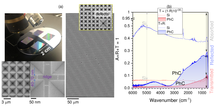
Electron beam definition of etch mask. We used conventional Si-wafers since IBC cell geometry is not compatible with SOI layer stacks. Cr masks were patterned by EBL to define PhC pattern with subsequent wet KOH etching. Figure 6(a) shows final PhC with m made on four regions. Chromium coating helped with charge removal and surface positioning (height) for EBL writing. Small ridges = 40-80 nm between neighboring inverted pyramids were obtained for longer KOH etch, however, more defects were observed when adjacent pyramids merged due to localised under etch. The number of defects was between 0.1 to 0.9%, calculated per pyramids. Figure 6(b) shows optical near-IR to IR performance of a m thick Si wafer patterned with the light trapping PhCs. The portions of reflected and transmitted parts of light intensity are from direct measurement and the absorbed portion is calculated from energy conservation . The PhC surface pattern caused a spectrally wide anti-reflection effect which contributed to the larger portion of absorbed energy. This evident from the difference between a patterned vs blank wafer spectra. Such surface can find applications in optical sensors (strong absorption) and emitters in the IR spectral range [22].
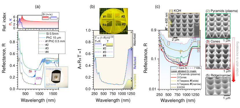
Figure 7 shows a summary of the spectral characterisation made of different samples in this study; reflectance from the stepper lithography prepared samples was reported in ref. [23], where the highest aspect ratio patterns showed the lowest reflectivity. Similar tendency was observed for the PhCs defined by the laser ablated and EBL defined masks (Figure 7). Figure 7(a-b) panels show high repeatability of spectra measured from four different regions of PhCs defined via EBL (a perfectly overlapping spectra). Reflectivity below 8% was obtainable for PhC defined by different methods as long as ridges were narrow and width of the tee-pee . The least reflective surface was observed from PhC structures which had corner regions between neighbouring tee-pee pits reaching the level of original Si surface (below Cr mask; see Figure S2(b)). They were among the deepest structures with m (marked as cones in Figure 7(c)). The tendency of reduction of reflectance with under etch, which also caused narrowest ridges , is apparent (see, SEM thumbnail images in (c)). When inverted pyramids were etched by wet KOH or dry plasma processing (6, 2 in (c)), was observed due significant contribution of original Si surface (at ridges) to reflectivity. Application of an antireflective coating for the final solar cell will provide further reduction of reflectance and is required passivisation for the reduction of the surface recombination rate. The most promising samples for the practical solar cells will be those with strongly under etched tee-pees due to their low reflectivity and maximum of the removed material which was at a Si-mask interface. The used plasma etch of Si was carried out at low-bias and low-power which makes only shallow nm surface modification, which is fully recoverable to almost pristine surface quality by different post-processing steps of annealing, \ceH2, \ceO2 treatments, or their combination, dependent on the used plasma chemistry [24, 25].
With optical the and measured experimentally, the absorbed part can be accessed. Then, the maximum achievable photo current density (MAPD) of the solar cell under AM1.5 (Figure 1(a)) illumination of intensity can be calculated [6]:
| (1) |
where the constants are: is the electron charge, is the Plank constant, is the speed of light. It is assumed that each absorbed photon creates a single electron-hole pair. Consequently, the short-circuit current for an ideal solar cell without losses due to surface and bulk recombination.How to achieve the latest conditions is an another wide field of research, which is already well matured and achieved world record efficiency in Si solar cell performance. Addition of PhC light trapping is a natural next step to improve light-to-electrical power conversion.
III Discussion
Laser patterning of a Cr or \ceAl2O3 mask has the fundamental advantage of not using vacuum chambers for the lithography step for pattern definition and can be up-scaled for large area fabrication. By combining high stage scanning speeds (10 cm/s and faster) with high repetition rates (200-600 kHz), it was possible to efficiently pattern cm2 surface areas within a reasonable hours time. Beam travel speeds of meters per second are in reach using galvano and polygon scanners. Synchronising the stage movement with laser repetition rate results in good alignment of the ablated sites between neighbouring lines, at expense of a slightly longer writing time. Different Cr thicknesses necessitate different pulse energies to open holes in the mask, but 20-60 nm Cr film can be ablated with good control of hole diameter with sub-20 nJ single pulses. Such pulse energies are now available from fs-laser oscillators and regenerative amplifiers are not required. Due to the almost 2× sized holes ablated by laser writing as compared with stepper photo-lithography defined mask, approximately 2× faster plasma etching was observed. Indeed, 4 mins was all that was needed to achieve optimal ridge conditions nm with the same optimised etching recipe for mask made by laser ablation.
In areas where there were missing holes at the laser ablation sites (missed pulse, slight change in spatial laser mode, etc.), an interesting pattern developed after under etch (Figure 3(b)). During the initial etch, the expected inverted pyramid pattern formed under the mask.When etching of the PhC pattern continued through to under etch, an upward pyramid was formed at the location where intended hole was not ablated. These unexpected defects are therefore favourable for the creation of deeper PhC patterns since the crystal orientation of the Si precludes aspect ratios much greater than 1. The results suggest that by creating a checkerboard hole pattern instead of a regular array, each inverted pyramid will be surrounded by four regular pyramids. The resultant PhC will have double the spatial frequency. This type of defect-mode can be intentionally designed to fabricate deeper PhC patterns and will be explored further.
Future studies will focus on changing the ratio of \ceSF6 to \ceCHF3 to affect the anisotropy (difference in etch rate between in x-y and z) during the dry etching [27]. Tilted angle etching of Si was tested [28], however, there was a strong difference in depth of the etched pattern at different distances from the electrode. Hence, using this method to control the shape of etched pits is less promising for PhC textured surfaces on solar cells even if predicts a close to Lambertian light trapping [29].
With RIE, varying the bias power greatly influences the etch anisotropy, which is important since the under-etch and aspect ratio can be controlled. Anisotropic etching at a larger bias creates deeper patterns, while isotoropic sideways etching is enhanced by a larger inductively coupled plasma (ICP) power. It was found that the bias voltage had little effect on the aspect ratio of inverted pyramids. The was observed (0.71 expected from Si lattice) and anisotropy of the Si etching was the defining property regardless bias used.
IV Conclusions and Outlook
Two different fabrication methods for large-area ( cm2) PhC patterns on Si for light trapping are demonstrated: 1) direct laser write and 2) stepper photo-lithography. They can scale up for light trapping solutions on order of magnitude larger surfaces and were compared with EBL, which recently showed close to the Lambertian limit performance over the visible spectral range and exceed it over 950-1200 nm wavelengths when an antireflection coating was applied on SOI samples [6]. In this study, large cm2 areas are demonstrated using a Cr etch mask on a Si wafer, rather than on SOI samples, making them more promising for integration with the most efficient IBC geometry solar cells.
Holes of 350-400 nm were opened in a Cr or \ceAl2O3 mask by single laser pulse irradiation, with writing speeds of 10 cm/s. Smaller holes with 180-245 nm diameter were fabricated in the Cr mask by the second method, stepper projection photo-lithography and lift-off. The plasma etching rate of Si vs hole diameter, , in Cr mask was sub-linear. Larger holes are vital for faster KOH etching, which is considerably longer h as compared with min for similar PhC patterns with RIE. Pulses of only 2-5 nJ (515 nm/230 fs) on the sample focused by a dry objective lenses are required for laser printing of nm diameter nano-holes in the Cr-mask; approximately double the pulse energy was required for opening holes in the \ceAl2O3 mask.
Due to strong under etch, the surface of Si where damage occurred during hole ablation is removed by plasma etch. A subsequent KOH or TMAH [30] etch step for Si surfaces can be added for the lowest SRV and best quality at the very end of PhC fabrication. Use of dielectric \ceAl2O3 mask is expected to help further reduction of SRV and simplify surface texturing steps.
Future improvement of large area fs-laser pattering could employ Bessel-like beams to increase tolerance to surface tracking [31] and adopt stitch-free laser writing [32]. The main advantage of direct laser writing is due to it’s vacuum-free mode of operation in mask definition. Over the last 20 years, the trend for the average power of ultra-short pulsed lasers has been to double every two years, analogous to Moore’s law scaling [33] as reported by Amplitude Ltd. lasers [34], i.e. the number of photons packed in time (power) scales like the transistors per area/volume on a chip. Flexibility of material processing by burst mode ablation [35, 36] has fueled larger-area m2 industrial applications such as hydrophobic and anti-ice surface treatments or injection mold texturing [37, 38]. Fast polygon scanners with beam travel speeds up to hundreds of meters per second have been implemented to disperse kW radiation power. These trends are promising for solar cell texturing on increasingly larger areas by direct laser writing demonstrated in this study.
V Experimental Section
The energy balance of the absorbed, reflected, and transmitted parts of light energy was calculated from the refractive index of solar cell material (Si in this study [26]) at the normal incidence as and . These expressions are valid for light incidence from air . The Beer - Lambert law defines the transmitted part in a single pass through thickness ; , where the optical density (absorbance ) is calculated from the transmittance as . From the known spectrum of Silicon permittivity , the efficiency of light harvesting by different Si solar cell thickness was estimated and compared with with the corresponding Lambertian limit. Three different methods to define a light trapping PhC pattern on Si solar cell surface are described next.
V.1 Femtosecond laser writing
Direct fs-laser writing by ablation of Cr-on-Si mask was carried out with a solid state Yb:KGW laser (Pharos, Light Conversion, Ltd. Vilnius, Lithuania) at the nm wavelength with fs pulses at repetition rate kHz. High precision mechanical stages with write speed up to 25 cm/s (Aerotech, GmbH. Pittsburgh, USA.) were used for the lateral in-plane (xy) translation of the sample during laser write. Axial (z) positioning of the focal spot onto Si surface was made by a high-precision stage mount of the objective lens. A software-hardware integration solution of the entire fs-fabrication unit was made by Altechna Ltd. Ablation was carried out with focusing using objective lens with numerical aperture (Mitutoyo) at a low pulse energy nJ (on the sample) with pulse-to-pulse separation for specified period of PhC from m to 3.1 m. The laser beam profile was measured utilising a Ophir Spiricon SP928 beam profiling camera.
Laser fabrication was carried out in air (cleanroom, class 1000). Crystalline c-Si (n-type; Phosphorus-doped) and intrinsic samples (University wafer)The conductivity and its type of Si was determined by the van der Pauw method with an Ecopia HMS-3000. There was no difference observed for the tested low conductivity intrinsic n- and p-type Si in terms of formation of the laser ablation patterns and PhC plasma etching.
All samples were cleaned in acetone and isopropyl alcohol (IPA) prior and post etching to minimise surface contamination. A Cr thin film deposition on Si was made by an electron beam evaporation (Kurt J. Lesker AXXIS system)A reactive ion etching (RIE) was carrier out with RIE-101iPH (Samco)equipped with a load-lock system. Structural and optical characterisation of laser ablated regions and PhC structures were carried out by the SEM operation mode of EBL writer (Raith EBL 150TWO).
V.2 Stepper photo-lithography
An i-line (365 nm) stepper NIKON NSR-2205i12D at Nano-Processing Facility (NPF) AIST, Tsukuba, Japan was used for this study. A reticle mask (inset in Figure 5(a)) consisting of four square regions with different PhC period, , between a square array of m diameter disks (a light block for positive resist) were designed over the uniform exposure field of cm2. The pattern was projected on a 6-inch Si wafer using a demagnification with repeated exposure using the i-line stepper. Each quarter segment was a cm2 area after the exposure (Figure 5(b)). This pattern formed the mask for etching the photonic crystals (PhC).
An adhesion promoter for photoresist Hexamethyldisilazane (HMDS) was applied on Si wafers by dip coating after which 700 nm of positive resist (PFI-38) was spin coated onto the 6-inch Si substrate.After pre-baking at 90∘ for one minute, an exposure of 25 regions over 6-inch Si wafer was carried automatically (step & repeat; inset in (b)). Different exposure time (sub-1 s) was programmed for each step to optimise the exposure dose ( mJ/cm2 is required to expose the resist). Post-exposure bake at 110∘ for 60 seconds was implemented. Development of resist after exposure was carried out for 10 seconds in NMD-3 2.38% tetramethylammonium hydroxide (TMAH). The unexposed regions were retained on Si after development and the wafer was diced into cm2 chips after development (Figure 5(a)). Then, e-beam evaporation of 50 nm of Cr was carried out as described in the previous section. By sonication for 30 min in acetone at room temperature, lift-off over the entire chip area was achieved. The mask was designed to obtain 400-nm-diameter pillars after development (corresponding to m disks on the reticle). The designed value was approximately twice the achievable resolution of 200 nm for the stepper used.
V.3 Electron beam lithography
A Vistec EBPG5000plusES EBL writer was used for definition of the KOH wet-etch masks. Two approaches were used, the first produced a \ceSi3N4 mask, the second produced a Cr mask. The first approach used a combination of LPCVD of \ceSi3N4, E-Beam Lithography (EBL) and Deep Reactive Ion Etching (DRIE) to transfer the patterns into the \ceSi3N4. The fabrication started from growing 250 nm \ceSi3N4 on both sides of an SOI substrate with 10 m-thick device layer (inset of Figure 1(c)). Both, plasma enhanced and low pressure chemical vapour deposition (PECVD LPCVD) were tested to form the mask layer. The LPCVD was chosen since it provided more homogeneous, low stress, and porous-free films. A positive ZEP520 EBL resist was used for patterning. The array of patterned squares was oriented to align with the Si wafer flat. After development, the EBL exposure left a grid pattern of unexposed ZEP520 outlining the exposed \ceSi3N4 square areas. The width of the outline made of unexposed ZEP520 resist was optimised in the design step considering the under-etch of Si below the mask. The resulting ZEP520 grid was used as a mask for DRIE of the \ceSi3N4 layer below. After DRIE and stripping the resist, the final mask consisted in a \ceSi3N4 grid pattern outlining exposed square areas of Si. Particular care was taken to fully open the patterned areas into the \ceSi3N4 in order to expose the Si underneath while preventing excessive etching of the Si substrate. After KOH etching, the \ceSi3N4 mask was removed with HF. The final device was cleaned with Piranha solution. Photo-lithography was used to define back-side locations for eventual Si etching using AZ-family resist followed by RIE etch of \ceSi3N4 and stripping of the residual resist mask.
In the second approach, a Cr mask was made by EBL, Cr e-beam evaporation and lift-off. This approach was carried out on 4-inch Si n-type Phosphorous-doped wafers with a resistivity of 1-10 cm ( sheet resistance measured by 4-probe method (Jandel RM3000)). The outline of the squares was defined by exposing a 300 nm-thick layer of PMMA resist, leaving after resist development an array of regularly spaced PMMA squares. The patterned grid was oriented to align with the wafer flat. The spaces between the PMMA square patterns were filled with Cr by e-beam evaporation. The excess Cr and unexposed resist was removed during lift-off process with acetone. The result was a grid mask of Cr outlining the exposed Si square areas. After KOH etching, the Cr mask was removed using Cr etchant solution. The final device was cleaned with Piranha solution.
V.4 Etching
For potassium hydroxide (KOH) etch, a solution was prepared using 2 litres of 30% KOH which was then saturated with isopropyl alcohol (IPA) (2 cm surface layer). Etching was carried out at C. The etch time was evaluated using an online calculator [39] for the known pattern to be etched. Level of p-doping strongly affected the etch time. The depth of the inverted pyramids was dependent on the period of the light trapping texture. For the base-angle of pyramid , the depth and the side-length at the central cross section of a pyramid . For the used m, the corresponding depth (for ridge-less inverted pyramids pattern) is m (the aspect ratios ). After etching the light trapping pyramidal texture, the front-side was protected by a Protek coating [40] before a back-side etch step through the SOI substrate. For thicker silicon ( m), the KOH solution was heated between 60-70∘C to reduce etch time. Characterisation of fabricated structures was carried out using scanning electron microscopy (SEM), Fourier transform IR micro-spectroscopy (VERTEX 70 Burker), and UV/Vis/NIR spectrometer (PerkinElmer Lambda 1050).
Plasma etching of tee-pee patterns was carried out with \ceSF6 50 sccm, \ceCHF3 10 sccm, \ceO2 10 sccm for 5 to 30 minutes (etch time dictated different structures); the RF ICP was 180 W, bias 0 W, He pressure 2.70 kPa at a process pressure of 2.5 Pa. Etching of black-Si was made by process: \ceSF6 77 sccm, \ceO2 100 sccm for 5 minutes at RF ICP 300 W, bias 5 W, He pressure 2.70 kPa and process pressure of 2 Pa.
References
- Wilson et al. [2020] G. M. Wilson, M. Al-Jassim, W. K. Metzger, S. W. Glunz, P. Verlinden, G. Xiong, L. M. Mansfield, B. J. Stanbery, K. Zhu, Y. Yan, J. J. Berry, A. J. Ptak, F. Dimroth, B. M. Kayes, A. C. Tamboli, R. Peibst, K. Catchpole, M. O. Reese, C. S. Klinga, P. Denholm, M. Morjaria, M. G. Deceglie, J. M. Freeman, M. A. Mikofski, D. C. Jordan, G. TamizhMani, and D. B. Sulas-Kern, “The 2020 photovoltaic technologies roadmap,” Journal of Physics D: Applied Physics 53, 493001 (2020).
- Jaeger-Waldau [2019] A. Jaeger-Waldau, “Pv status report 2019,” in Publications Office of the European Union, Luxembourg (2019).
- Green et al. [2021] M. Green, E. Dunlop, J. Hohl-Ebinger, M. Yoshita, N. Kopidakis, , and X. Hao, “Solar cell efficiency tables (version 57),” Progress Photovoltaics: Res. Appl. 29, 3–15 (2021).
- Shockley and Queisser [1961] W. Shockley and H. J. Queisser, “Detailed Balance Limit of Efficiency of p‐n Junction Solar Cells,” Journal of Applied Physics 32, 510–519 (1961).
- Bhattacharya and John [2019] S. Bhattacharya and S. John, “Beyond 30% conversion efficiency in silicon solar cells: A numerical demonstration,” Scientific Reports 9, 12482 (2019).
- Hsieh et al. [2020] M.-L. Hsieh, A. Kaiser, S. Bhattacharya, S. John, and S.-Y. Lin, “Experimental demonstration of broadband solar absorption beyond the lambertian limit in certain thin silicon photonic crystals,” Sci. Rep. 10, 11857 (2020).
- Bhattacharya et al. [2019] S. Bhattacharya, I. Baydoun, M. Lin, and S. John, “Towards 30% power conversion efficiency in thin-silicon photonic-crystal solar cells,” Phys. Rev. Applied 11, 014005 (2019).
- Simovski and Tretyakov [2020] C. Simovski and S. Tretyakov, “Nanostructures for enhancement of solar cells,” in An Introduction to Metamaterials and Nanophotonics (Cambridge University Press, 2020) p. 245–303.
- Yamaguchi et al. [2020] M. Yamaguchi, K.-H. Lee, D. Sato, K. Araki, N. Kojima, T. Takamoto, T. Masuda, and A. Satou, “Overview of Si tandem solar cells and approaches to PV-powered vehicle applications,” MRS Advances 5, 441 – 450 (2020).
- am1 [2021] https://www.nrel.gov/grid/solar-resource/spectra-am1.5.html (2021), online; accessed 1 April 2021.
- Hollemann et al. [2019] C. Hollemann, F. Haase, S. Schäfer, J. Krügener, R. Brendel, and R. Peibst, “26.1%‐efficient POLO‐IBC cells: Quantification of electrical and optical loss mechanisms,” Sol. Energ. Mat. Sol. Cells 27, 950–958 (2019).
- Green [2009] M. A. Green, “The path to 25silicon solar cell efficiency: History of silicon cell evolution,” Progress in Photovoltaics: Research and Applications 17, 183–189 (2009).
- Nishijima et al. [2016] Y. Nishijima, R. Komatsu, S. Ota, G. Seniutinas, A. Balcytis, and S. Juodkazis, “Anti-reflective surfaces: Cascading nano/microstructuring,” APL Photonics 1, 076104 (2016).
- J.Y.-H.Chai, Wong, and S.Juodkazis [2020] J.Y.-H.Chai, B. Wong, and S.Juodkazis, “Black-silicon assisted photovoltaic cells for better conversion efficiencies: A review on recent research and development efforts,” Materials Today Energy 18, 100539 (2020).
- P.Ščajev et al. [2016] P.Ščajev, T. Malinauskas, G. Seniutinas, M. Arnold, A. Gentle, I. Aharonovich, G. Gervinskas, P. Michaux, J. Hartley, E. Mayese, P. Stoddart, and S. Juodkazis, “Light-induced reflectivity transients in black-Si nanoneedles,” Solar Energy Materials and Solar Cells 144, 221–227 (2016).
- Peibst [2021] R. Peibst, “Still in the game,” Nature Energy 6, 333–334 (2021).
- Richter et al. [2021] A. Richter, R. Müller, J. Benick, F. Feldmann, B. S. C. Reichel, A. Fell, M. Bivour, M. Hermle, and S. W. Glunz, “Design rules for high-efficiency both-sidescontacted silicon solar cells with balanced charge carrier transport and recombination losses,” Nature Energy 6, 429–438 (2021).
- Köhler et al. [2021] M. Köhler, M. Pomaska, P. Procel, R. Santbergen, A. Zamchiy, B. Macco, A. Lambertz, W. Duan, P. Cao, B. Klingebiel, S. Li, A. Eberst, M. Luysberg, K. Qiu, O. Isabella, F. Finger, T. Kirchartz, U. Rau, and K. Ding, “A silicon carbide-based highly transparent passivating contact for crystalline silicon solar cells approaching efficiencies of 24%,” Nature Energy 6, 529–537 (2021).
- Bonse et al. [2002] J. Bonse, S. Baudach, J. Krüger, W. Kautek, and M. Lenzner, “Femtosecond laser ablation of silicon–modification thresholds and morphology,” Applied Physics A 74, 19–25 (2002).
- Wolff et al. [2009] C. H. Wolff, S. Whitlock, R. M. Lowe, A. I. Sidorov, and B. V. Hall, “Fabricating atom chips with femtosecond laser ablation,” J. Phys. B: At. Mol. Opt. Phys. 42, 085301 (2009).
- Kirchner et al. [2020] R. Kirchner, V. Neumann, F. Winkler, C. Strobel, S. Völkel, A. Hiess, D. Kazazis, U. Künzelmann, and J. W. Bartha, “Anisotropic etching of pyramidal silica reliefs with metal masks and hydrofluoric acid,” Small 16, 2002290 (2020).
- Nishijima et al. [2019] Y. Nishijima, A. Balcytis, S. Naganuma, G. Seniutinas, and S. Juodkazis, “Kirchhoff’s metasurfaces towards efficient photo-thermal energy conversion,” Scientific Reports 9, 8284 (2019).
- Maksimovic et al. [2021] J. Maksimovic, J. Hu, S. H. Ng, T. Katkus, G. Seniutinas, Y. Nishijima, S. John, and S. Juodkazis, “Large area cm2 light trapping patterns for Si solar cells,” in Advanced Fabrication Technologies for Micro/Nano Optics and Photonics XIV, Vol. 11696, edited by G. von Freymann, E. Blasco, and D. Chanda, International Society for Optics and Photonics (SPIE, 2021) pp. 57 – 68.
- Misra and Heasell [1990] D. Misra and E. L. Heasell, “Electrical damage to silicon devices due to reactive ion etching,” Semicond. Sci. Technol. 5, 229–236 (1990).
- Mu et al. [1986] X. C. Mu, S. J. Fonash, G. S. Oehrlein, S. N. Chakravarti, C. Parks, and J. Keller, “A study of CClF3/H2 reactive ion etching damage and contamination effects in silicon,” J. Appl. Phys. 59, 2958 (1986).
- Green [2008] M. A. Green, “Self-consistent optical parameters of intrinsic silicon at 300K including temperature coefficients,” Sol. Energ. Mat. Sol. Cells 92, 1305–1310 (2008).
- Kuang et al. [2016] P. Kuang, S. Eyderman, M.-L. Hsieh, A. Post, S. John, and S.-Y. Lin, “Achieving an accurate surface profile of a photonic crystal for near-unity solar absorption in a super thin-film architecture,” ACS Nano 10, 6116–6124 (2016).
- Gailevičius et al. [2020] D. Gailevičius, M. Ryu, R. Honda, S. Lundgaard, T. Suzuki, J. Maksimovic, J. Hu, D. Linklater, E. Ivanova, T. Katkus, V. Anand, M. Malinauskas, Y. Nishijima, S.-H. Ng, K. Staliūnas, J. Morikawa, and S. Juodkazis, “Tilted black-Si: 0.45 form-birefringence from sub-wavelength needles,” Optics Express 28, 16012–16026 (2020).
- Han and Chen [2010] S. E. Han and G. Chen, “Toward the lambertian limit of light trapping in thin nanostructured silicon solar cells,” Nano Lett. 10, 4692–4696 (2010).
- Fan et al. [2013] Y. Fan, P. Han, P. Liang, Y. Xing, Z. Ye, and S. Hu, “Differences in etching characteristics of TMAH and KOH on preparing inverted pyramids for silicon solar cells,” Applied Surface Science 264, 761–766 (2013).
- Mikutis et al. [2013] M. Mikutis, T. Kudrius, G. Šlekys, D. Paipulas, and S. Juodkazis, “High 90% efficiency bragg gratings formed in fused silica by femtosecond gauss-bessel laser beams,” Optical Materials Express 3, 1862–1871 (2013).
- Jonušauskas et al. [2019] L. Jonušauskas, D. Gailevičius, S. Rekštytė, T. Baldacchini, S. Juodkazis, and M. Malinauskas, “Mesoscale laser 3d printing,” Optical Express 27, 15205–15221 (2019).
- Han et al. [2021] M. Han, D. Smith, S.-H. Ng, V. Anand, T. Katkus, and S. Juodkazis, “Ultra-short pulse lasers – materials - applications,” in Proceedings of the 2nd International Electronic Conference on Applied Sciences, 15–31 October 2021 (MDPI, Basel, Switzerland,, 2021).
- Mottay [2021] E. Mottay, “Femtosecond lasers for high throughput surface engineering,” in SPIE Photonics West Industry, Vol. 11768 (SPIE, Bellingham, Washington, USA, 2021) pp. 11768–07.
- Kerse et al. [2016] C. Kerse, H. Kalaycıoǧlu, P. Elahi, B. Çetin, D. Kesim, O. Akçaalan, S. Yavaş, M. Aşık, B. Öktem, H. Hoogland, R. Holzwarth, and F. Ilday, “Ablation-cooled material removal with ultrafast bursts of pulses,” Nature 537, 84–88 (2016).
- Förster et al. [2021] D. Förster, B. Jäggi, A. Michalowski, and B. Neuenschwander, “Review on experimental and theoretical investigations of ultra-short pulsed laser ablation of metals with burst pulses,” Materials 14, 3331 (2021).
- Bonaccurso [2021] E. Bonaccurso, “Laser-treated superhydrophobic surfaces to reduce ice build-up in aeronautical applications,” in SPIE Photonics West Industry, Vol. 11768 (SPIE, Bellingham, Washington, USA, 2021) pp. 11768–0M.
- Hodgson et al. [2021] N. Hodgson, A. Steinkopff, S. Heming, H. Allegre, H. Haloui, T. Lee, M. Laha, and J. VanNunen, “Ultrafast laser machining: process optimization and applications,” in SPIE Laser Applications in Microelectronic and Optoelectronic Manufacturing (LAMOM) XXVI, Vol. 11673 (SPIE, Bellingham, Washington, USA, 2021) pp. 11673–08.
- KOH [2020] http://www.lelandstanfordjunior.com/KOH.html (2020), online; accessed 1 January 2020.
- Pro [2020] https://www.brewerscience.com/products/protective-coatings/ (2020), online; accessed 1 January 2020.
- Gokhale and Abbaschian [1987] A. B. Gokhale and G. J. Abbaschian, “The Cr-Si chromium-silicon system,” J. Phase Equilibria 8, 474–484 (1987).
- Vailionis et al. [2011] A. Vailionis, E. Gamaly, V. Mizeikis, W. Yang, A. Rode, and S. Juodkazis, “Evidence of superdense aluminium synthesized by ultrafast microexplosion,” Nature Comm. 2, 445 (2011).
- Juodkazis et al. [2006] S. Juodkazis, K. Nishimura, H. Misawa, T. Ebisui, R. Waki, S. Matsuo, and T. Okada, “Control over the crystalline state of sapphire,” Adv. Mat. 18, 1361–1364 (2006).
Acknowledgements.
We are grateful for project support by Nano-Processing Facility (NPF), AIST, Tsukuba, Japan where we were granted access to photo-lithography stepper. This work was granted by ARC DP190103284 ”Photonic crystals: the key to breaking the silicon-solar cell efficiency barrier” project. S. Juodkazis is grateful to the visiting professor program at the Institute of Advanced Sciences at Yokohama National University (2018-20) and to Nanotechnology Ambassador fellowship at MCN (2012-19). This work was performed in part at the Melbourne Centre for Nanofabrication (MCN) in the Victorian Node of the Australian National Fabrication Facility (ANFF). We thank Workshop-of-Photonics (WOP) Ltd., Lithuania for patent licence and technology transfer project by which the industrial fs-laser fabrication setup was acquired for Nanolab, Swinburne. We are grateful to Dan Kapsaskis and An Lee for the training at the characterisation facility.Supporting Information
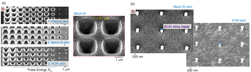
A flow chart of PhC fabrication on Si surface is shown in Figure S1(a) and the final result for fs-laser fabrication in (b). Figure S2 summarises structural changes during plasma etching through different diameter holes which were laser ablated through Cr film. Different reactive ion etching (RIE) protocols were tested with a Cr mask with nm holes obtained using a stepper lithography followed by lift-off (Figure 5). An optimised RIE procedure to obtain etched pits with the aspect ratio close to one was carried out at flow rates of \ceSF6 50 sccm, \ceCHF3 10 sccm, \ceO2 10 sccm (at bias 5 W) for 7 min; the inductively coupled plasma (ICP) power was 180 W, pressure 5 Pa ( 37.5 mTorr). It is noteworthy that the aspect ratio of KOH etch Si is 0.71 for the inverted pyramids on Si(100) surface. Figure S4 shows SEM images of etched patterns after removal of Cr mask. By defining the opening width of the etched Si pit, , ratio to the period of the pattern, , it is possible to establish the required etching protocol. Final PhC pattern should have minimum width of the ridges between adjacent etched inverted pyramids, which corresponds to the condition or . Inset plot in Figure S4 shows a linear dependence for the for the patterns etched in the same run at the etch time of min. The shape of plasma etched inverted pyramids was apparently different (Figure S4) resembling KOH-etched shape defined by the crystalline structure of Si for m while showing tee-pee structure for larger .
Figure S5 shows results of Si initially etched by RIE then with different dry and wet etching treatments applied. It was observed that with the smallest pulse energy of nJ, there were no ablation opening but a noticeable surface modification took place. Plasma etching, which produced a nanotextured black-Si surface was applied to reveal structural modifications on the Cr mask at the low energy laser pulses (see Figure S5 (b)). Those regions acted as a mask and prevented surface etching. The mask is expected to be Si:Cr nano-alloy which can have different compositions depending on the formation at the higher temperatures close to the Cr melting at 1860∘C or that of Si at 1414∘C [41]. As shown in Section II, the largest part of laser pulse energy is deposited into Cr. Hence high temperature phases of Cr-rich alloy are expected Cr3Si, -Cr5Si3 and -Cr5Si3 [41] since they are formed at higher temperatures. However, due to an ultra-fast thermal quenching of the alloy due to a very small volume, formation of non-equilibrium phases of the melt are possible, as was observed for bulk damage of materials with ultra-short laser pulses [42]. In such a case, Si-rich phases are also possible since they are formed at lower temperatures (closer to the Si-Cr interface): CrSi and CrSi2; interestingly, the latter is a thermoelectric material [41]. Phases such as amorphous-Al2O3, which are not existent at room conditions, can be formed under tightly focused fs-laser pulses [43], hence an amorphous Si:Cr nano-alloys can be expected. A separate study is planned to investigate nano-alloy formation at the conditions used.