Correlations in the Electronic Structure of van der Waals NiPS3 Crystals: An X-Ray Absorption and Resonant Photoelectron Spectroscopy Study
Abstract
The electronic structure of high-quality van der Waals NiPS3 crystals was studied using near-edge x-ray absorption spectroscopy (NEXAFS) and resonant photoelectron spectroscopy (ResPES) in combination with density functional theory (DFT) approach. The experimental spectroscopic methods, being element specific, allow to discriminate between atomic contributions in the valence and conduction band density of states and give direct comparison with the results of DFT calculations. Analysis of the NEXAFS and ResPES data allows to identify the NiPS3 material as a charge-transfer insulator. Obtained spectroscopic and theoretical data are very important for the consideration of possible correlated-electron phenomena in such transition-metal layered materials, where the interplay between different degrees of freedom for electrons defines their electronic properties, allowing to understand their optical and transport properties and to propose further possible applications in electronics, spintronics and catalysis.
SHU]
Department of Physics, Shanghai University, 200444 Shanghai, China
SHU]
Department of Physics, Shanghai University, 200444 Shanghai, China
SHU]
Department of Physics, Shanghai University, 200444 Shanghai, China
SFedU]
Institute of Physical and Organic Chemistry, Southern Federal University,
344090 Rostov on Don, Russia
FUB]
Institut für Chemie und Biochemie, Freie Universität Berlin, Arnimallee 22,
14195 Berlin, Germany
TUDD]
Institut für Festkörper- und Materialphysik, Technische Universität Dresden,
01069 Dresden, Germany
SHU]
Department of Physics, Shanghai University, 200444 Shanghai, China
\alsoaffiliation[FUB]
Institut für Chemie und Biochemie, Freie Universität Berlin, Arnimallee 22,
14195 Berlin, Germany
SHU]
Department of Physics, Shanghai University, 200444 Shanghai, China
\alsoaffiliation[FUB]
Institut für Chemie und Biochemie, Freie Universität Berlin, Arnimallee 22,
14195 Berlin, Germany
![[Uncaptioned image]](/html/2112.13732/assets/ToC_figure.jpg)
Layered materials, like graphene, silicene or transition metal dichalcogenides (TMDs) and different heterosystems on their basis have attracted much attention in the last years 1, 2, 3, 4, 5, 6. These studies are motivated by the hope on the possible new applications of these materials in different areas, where their unique electronic and transport properties might bring new functionalities. These layered materials can be relatively easily produced in the high quality form either as bulk materials or as a monolayer (or multilayer) on different substrates and then isolated for further studies or applications 7, 8, 9, 10, 11, 12. Such high-quality layers and heterosystems made from layered 2D materials allow to perform studies of different intriguing collective quantum phenomena, which appear in low-dimensional systems, like, for example, superconductivity for twisted graphene bi-layers 13, 14, charge density waves in TMDs 15, 16, and coherent excitonic excitations in antiferromagnetic transition metal trichalcogenide (TMT) NiPS3 17. For example, recently, different exciting phenomena in 2D materials were extended to the observation of the long-range Ising-type antiferromagnetic (AFM) order in the TMT FePS3 monolayer with a Néel temperature () of K 18, 19. Following these works, a layer-dependent ferromagnetic (FM) order in CrI3 with a Curie temperature () of K was reported 20 and then the FM magnetic order has been observed for single atomic layers of Cr2Ge2Te6 ( K) 21, Fe3GeTe2 ( K) 22, and MnSe2 23. These inspiring discoveries of magnetic order in 2D monolayers open up exciting opportunities for the application of these properties in new transport and optical devices and for the exploration of intrinsic 2D Ising-type (anti)ferromagnetism.
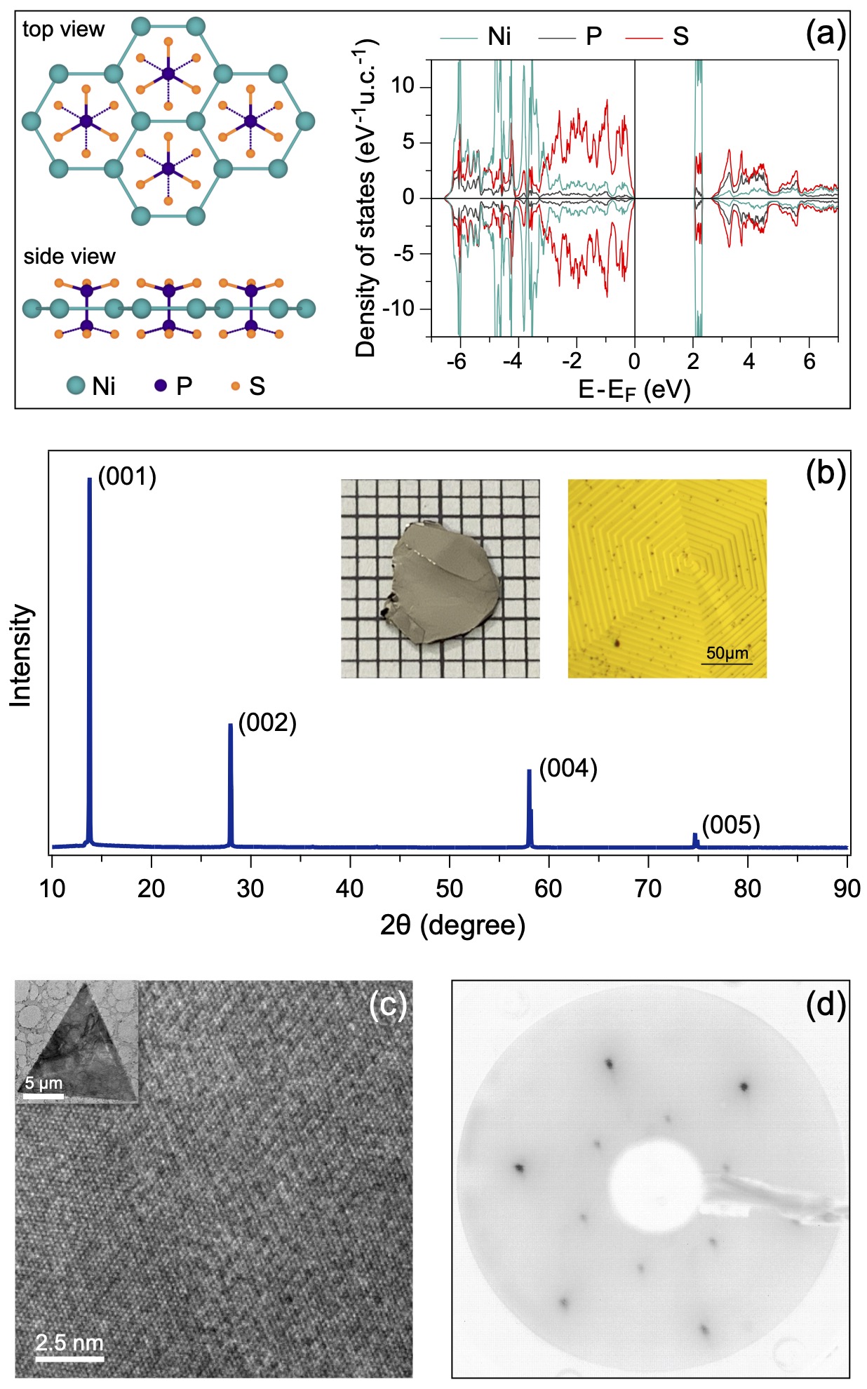
The above mentioned layered transition metal trichalcogenides (TMPX3; TM: TMs, like Fe, Co, or Ni; X: chalcogen, like S or Se) came to the focus of the studies of 2D materials only recently 24, 25, 26. From the crystallographic point of view they can be seen as layers of TMS2 where one third of TM atoms is replaced by P–P dimers perpendicular to the layer (Fig. 1(a)) and in the 3D structure they crystalize into the or space groups 27, 28. Most of these compounds are AFM wide-gap semiconductors 29, 30, 28 and they were proposed for different applications like gas sensors, optical sensors, effective materials in water splitting applications and in (opto)spintronics 31, 32, 26. Surprisingly, at the present time, the main focus in the studies of this class of materials is concentrated on the applied-oriented investigations, missing the systematic studies of their electronic structure using different electron spectroscopy methods, which provide direct insight in these properties. Such experiments can give a direct comparison with the available theoretical data and link them to the available application-oriented studies, providing the route to improve their properties 33.
Here, we present systematic x-ray photoelectron spectroscopy studies of the representative TMT layered material, NiPS3. Using density functional theory (DFT) calculations, it is shown that NiPS3 is an AFM semiconductor in its ground state. It has a band gap of more than eV and the magnetic properties of this material are described with a model Hamiltonian of the XY-type. Near-edge x-ray absorption spectroscopy (NEXAFS) and resonant photoelectron spectroscopy (ResPES) performed around the respective absorption edges allow to discriminate between different atomic contributions in the density of states (DOS) for valence and conduction bands. Our analysis of the NEXAFS and ResPES data for the Ni absorption edge indicate that NiPS3 can be described as a charge-transfer insulator according to the Zaanen-Sawatzky-Allen scheme with strong correlation effects in the valence band of this material. Details describing experimental and theoretical approaches used in the present study as well as additional data are presented in the Supplementary Information.
Layered NiPS3 bulk crystals in our study were synthesized using chemical vapor transport (CVT) method from the stoichiometric amounts of elements and obtained several- samples were characterized using different bulk- and surface-sensitive techniques. Fig. 1(b,c) show x-ray diffraction (XRD) plot, optical images and transmission electron microscopy (TEM) data for NiPS3 crystal and these data are in perfect agreement with referenced and previously published data 27, 34, 35 demonstrating high-quality of samples studied in the present work (see also Fig. S1 and Fig. S2 in Supplementary Information for the high-resolution cross-section TEM images and energy dispersive x-ray (EDX) analysis data collected in the TEM measurements, respectively). The distance between single layers of NiPS3 extracted from the high-resolution TEM data is Å, which is in very good agreement with the value of Å obtained in our DFT calculations for fully relaxed 3D structure. [The complete crystallographic data for the fully optimized 3D structure of NiPS3 are presented in Table S3.] Raman spectra of NiPS3 are shown in Fig. S4 of Supplementary Information and also in very good agreement with previously presented results, which were used for the assignment of the observed scattering peaks 36, 37, 34, 38.
NiPS3 was characterized using different surface-sensitive methods and Fig. 1(d) presents low-energy electron diffraction (LEED) image of the freshly-cleaved and UHV-degassed sample. It shows clear hexagonal diffraction spots, which are due to the hexagonal unit cell of NiPS3 in the -plane perpendicular to the impinge electron beam. The presented LEED image was collected in the low-current electron-beam regime at the primary electron energy of eV indicating high surface crystallographic quality with long-range order. Our reference measurements using Au-crystal allow to conclude that presented image shows 1st and 2nd diffraction orders for the NiPS3 -surface.
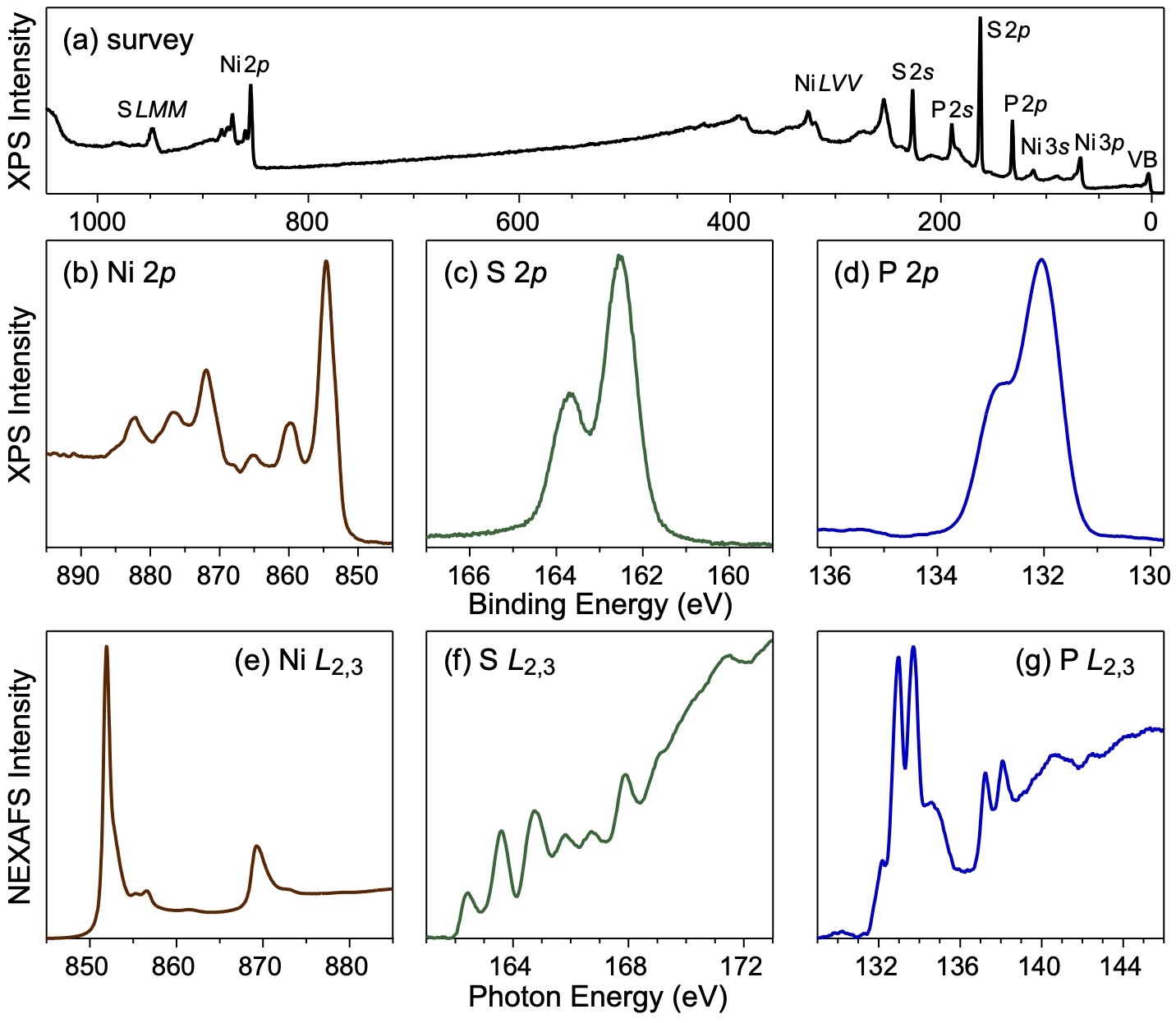
The results of x-ray photoelectron spectroscopy (XPS) characterization and NEXAFS measurements at the Ni, S, and P absorption edges for NiPS3 are summarized in Fig. 2. Survey XPS spectrum measured for NiPS3 shows a series of characteristic emission peaks (without any additional emission lines from possible contaminants), which can be easily identified, and they are marked in panel (a). The characteristic multiplet structure for the Ni spectrum (Fig. 2(b)) is in very good agreement with the recent data for NiPS3 39 and NiGa2S4 40, where multiplet modeling using the NiS6 cluster gives the dominant Ni ground state in both cases ( marks the hole on the ligand site). S and P XPS spectra (Fig. 2(c,d)) demonstrate clear single spin-orbit-slit doublets indicating strongly localized covalent bonds between P and S atoms forming (P2S6)4- anions.
The Ni NEXAFS spectrum (Fig. 2(e) and Fig. 3(a)) demonstrates characteristic absorption edge for two spin-orbit split components separated by eV. According to the Zaanen-Sawatzky-Allen scheme for transition-metal compounds (insulators and semiconductors) 41, their electronic structure can be described with two parameters, the correlation energy () and charge transfer energy between -states of metal and -states of ligand (). Simplifying all considerations, one can say that if , then compound is the Mott-Hubbard type insulator, while it is the charge-transfer type insulator if . For NiPS3 the Ni NEXAFS spectra were simulated in Ref. 39 and good agreement with experimental data was suggested for eV and eV, indicating that this compound is the so-called self-doped negative charge-transfer insulator. In our simulations (see computational details and Fig. S5 in Supplementary Information) using eV, the best fit is achieved for charge transfer energy between eV and eV giving simple charge-transfer insulating state for NiPS3. Besides the correctly shown two-peaks satellite structure above the absorption edge, with these parameters our simulations also correctly reproduce the high-energy shoulder for these line as well as all fine structures in the NEXAFS spectra. Our DFT calculations with eV lead to the correct crystallographic structure of NiPS3 with simultaneous adequately reproduced value for K (vs. K obtained in the experiment 42). In this case, the respective value for the occupation number for orbitals of the Ni2+ ion is and the calculated value for magnetic moment of Ni ions is closer to the formal value of compared to the previously reported results 39. Our DFT calculations also give significantly wider band gap for NiPS3 – 2.19 eV (vs. eV in Ref. 39) together with correctly calculated optical absorption spectra (see Fig. S6 in Supplementary Information). Also our DFT calculations give the different distribution of the PDOS in the valence band compared to the previous results (see Fig. 1(a) and Fig. S7 for present DFT results obtained using PBED2 and HSE06+D2 functionals, respectively). One has to note that value eV was recently obtained during correct simulation of the resonant inelastic x-ray scattering spectra of NiPS3 17 supporting our results.
The S and P NEXAFS spectra of NiPS3 shown in Fig. 2(f) and (g), respectively, have a very rich structure consisting of sharp peaks. These spectra reflect the transitions from the ligand spin-orbit split and core levels onto the unoccupied and states. The interpretation of these spectra is quite tedious and ambiguous procedure, however one can conclude that the sharp double-peak structure in the S ( eV and eV) and P ( eV and eV) spectra reflects the electron transitions into the first unoccupied hybrid -like antibonding state formed by S and P 43, 44. The first peak in the S spectrum at eV and the respective shoulder in the P spectrum at eV most probably correspond to the states in the conduction band peaked at eV. Further peaks in the NEXAFS spectra observed at higher photon energies can be assigned either to the so-called “echo” or shadow effect of the spin-orbit split features due to multiple scattering or to electron transitions to a mixed-valence band states 43, 44, 45.
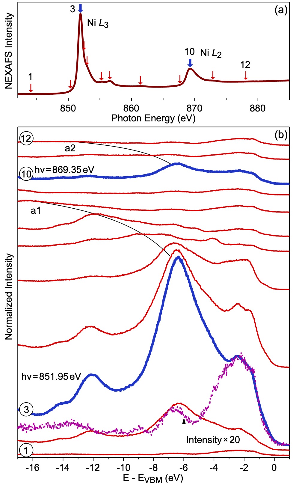
The results of the ResPES measurements at the Ni absorption edge for NiPS3 are presented in Fig. 3, supporting the description of this material as the charge-transfer insulator: In panel (a) the reference Ni NEXAFS spectrum is shown and in panel (b) a series of photoemission spectra taken at the particular photon energies marked by the vertical arrows in (a) is presented. Previous considerations of the transition metal oxides and sulfides 46, 47, 48, 49, 50 show that in case of the Mott-Hubbard insulator with (e. g., Mn and Fe oxides) the core-level and valence band XPS spectra consist of the low-binding-energy intense peak originated mainly from the final state and the satellite structure at larger binding energies. For the charge-transfer insulator with (e. g., Ni oxide), the low-binding-energy intense peak is formed by the configuration mixing of the and final states ( is the bound states; e. g., for NiO its a Zhang-Rice doublet bound states) 50 and the peak associated with the final state is located at larger binding energies with smaller intensities. (Here one has to note that strong hybridization between two final states does not allow to clearly separate them in the photoemission spectra of the valence band region, requiring detailed fitting of the experimental data using cluster model calculations.)
In the ResPES measurements at the Ni absorption edge for NiPS3 the photoemission intensity is the result of interference of two emission channels 51: (i) a direct photoemission and (ii) a photoabsorption process followed by a participator Coster-Kronig decay and the initial and final states for these two photoemission channels are identical. Also the interference between these excitation channels leads to the Fano-type resonance for states with the final-state character 51. For the ResPES experiments the second emission channel (Coster-Kronig decay) prevails in the spectra, therefore giving the position of the peak relative to the position of the line.
The off-resonance spectrum of NiPS3 measured at eV (spectrum in Fig. 3(b) and its intensity multiplied by factor 20 is shown by the dotted line) demonstrates a broad two-peaks structure in the range of eV and additional satellite structure at larger binding energies. If we assume that NiPS3 is a charge-transfer insulator with (according to the previous considerations and considering the similar ion state for charge-transfer insulating state of NiO), then the first structure can be assigned to the final state and other peaks to the final state. The on-resonance photoemission spectrum measured with the photon energy eV corresponding to the absorption edge (spectrum in Fig. 3(b)) demonstrates the drastic increase of the photoemission intensity by factor of for the two-peaks structure in the range eV and by factor of for the peaks at large binding energies. However, as it was discussed earlier, in the ResPES experiments the Coster-Kronig decay channel mainly contributes in the photoemission spectra. Thus we can conclude that the huge peak at eV and the additional satellites structure at eV correspond to the final state and confirm that NiPS3 has to be described as the charge-transfer insulator material. The similar consideration is valid for the on-resonance photoemission spectrum measured at the absorption edge (spectrum in Fig. 3(b)). The obtained results which allow to describe NiPS3 as charge-transfer insulator are supported by the DFT results. In the DOS plot (Fig. 1(a)), the top of the valence band is dominated by the S states with the Ni states spreading between eV and eV. At the same time the bottom of the conduction band is formed mainly by unoccupied Ni states, leading to the description of NiPS3 as a charge-transfer insulator according to the Zaanen-Sawatzky-Allen scheme (see Fig. S8) and confirming experimental spectroscopic results. [Here we have to note that the correct simulation of the ResPES spectra on the basis of the available DOS data is only possible in the many-electron approximation, which might be a topic for further studies.] The presented results are in a rather good agreement with the experimental and calculated ResPES spectra of NiO (Ni2+) in the charge-transfer insulating state, where similar spectral behavior was found 49, 50.
In summary, we performed systematic studies of the crystallographic structure and electronic properties of layered van der Waals material NiPS3 using different ex situ and in situ UHV surface science techniques, including LEED and electron spectroscopy methods, like XPS, NEXAFS and ResPES. Our structural investigations demonstrate very high quality of the studied crystals allowing to obtain clear diffraction spots for the freshly-cleaved surface of insulating NiPS3. Further results obtained using electron spectroscopy methods indicate strong correlations effects in this material and we show that all electron spectroscopy data can be successfully described using cluster based approach for the Ni2+ ion in octahedral field. NEXAFS Ni data show that NiPS3 can be described as a transfer-charge insulator with . This is also supported by the systematic ResPES data collected around the Ni absorption edge, which clearly demonstrate the strong resonant behavior for the photoemission final state. As deduced from these data, this final state is located at large binding energies compared to those for final state located at the top of the valence band. The present results are first systematic electron spectroscopy data allowing to understand the electronic structure of these new layered materials and are of paramount importance for the further studies giving a strong basis for the understanding their transport, optical, and catalytic properties.
This work was supported by the National Natural Science Foundation of China (Grant No. 21973059). A.M. acknowledges the BMBF (grant No. 05K19KER). D.S. acknowledges the BMBF (grant no. 0519ODR). A.T. acknowledges the Ministry of Science and Higher Education of the Russian Federation no. 0852-2020-0019 (State assignment in the field of scientific activity, Southern Federal University, 2020 project no. BAZ0110/20-1-03EH) and resources of the center of the collective use of SFedU “High-Resolution Electron Microscopy”. We thank HZB for the allocation of synchrotron radiation beamtime and for support within the bilateral Russian-German Laboratory program. The North-German Supercomputing Alliance (HLRN) is acknowledged for providing computer time.
The following files are available free of charge
-
•
Description of experimental methods, sample preparation and DFT calculations. Additional experimental and theoretical data (PDF) can be downloaded via link: https://pubs.acs.org/doi/10.1021/acs.jpclett.1c00394
References
- Geim 2009 Geim, A. Graphene: Status and Prospects. Science 2009, 324, 1530–1534
- Das Sarma et al. 2011 Das Sarma, S.; Adam, S.; Hwang, E. H.; Rossi, E. Electronic Transport in Two-Dimensional Graphene. Rev. Mod. Phys. 2011, 83, 407–470
- Geim and Grigorieva 2014 Geim, A. K.; Grigorieva, I. V. Van der Waals Heterostructures . Nature 2014, 499, 419–425
- Zhuang et al. 2015 Zhuang, J.; Xu, X.; Feng, H.; Li, Z.; Wang, X.; Du, Y. Honeycomb Silicon: A Review of Silicene. Sci. Bull. 2015, 60, 1551–1562
- Carvalho et al. 2016 Carvalho, A.; Wang, M.; Zhu, X.; Rodin, A. S.; Su, H.; Castro Neto, A. H. Phosphorene: From Theory to Applications. Nat. Rev. Mater. 2016, 1, 16061
- Manzeli et al. 2017 Manzeli, S.; Ovchinnikov, D.; Pasquier, D.; Yazyev, O. V.; Kis, A. 2D Transition Metal Dichalcogenides. Nat. Rev. Mater. 2017, 2, 17033
- Bae et al. 2010 Bae, S.; Kim, H.; Lee, Y.; Xu, X.; Park, J.-S.; Zheng, Y.; Balakrishnan, J.; Lei, T.; Kim, H. R.; Song, Y. I. et al. Roll-to-Roll Production of 30-inch Graphene Films for Transparent Electrodes. Nat. Nanotech. 2010, 5, 574–578
- Chhowalla et al. 2013 Chhowalla, M.; Shin, H. S.; Eda, G.; Li, L.-J.; Loh, K. P.; Zhang, H. The Chemistry of Two-Dimensional Layered Transition Metal Dichalcogenide Nanosheets. Nat. Chem. 2013, 5, 263–275
- Ryu et al. 2014 Ryu, J.; Kim, Y.; Won, D.; Kim, N.; Park, J. S.; Lee, E.-K.; Cho, D.; Cho, S.-P.; Kim, S. J.; Ryu, G. H. et al. Fast Synthesis of High-Performance Graphene Films by Hydrogen-Free Rapid Thermal Chemical Vapor Deposition. ACS Nano 2014, 8, 950–956
- Dedkov and Voloshina 2015 Dedkov, Y.; Voloshina, E. Graphene Growth and Properties on Metal Substrates. J. Phys.: Condens. Matter 2015, 27, 303002
- Li et al. 2018 Li, H.; Li, Y.; Aljarb, A.; Shi, Y.; Li, L.-J. Epitaxial Growth of Two-Dimensional Layered Transition-Metal Dichalcogenides: Growth Mechanism, Controllability, and Scalability. Chem. Rev. 2018, 118, 6134–6150
- Dedkov and Voloshina 2020 Dedkov, Y.; Voloshina, E. Epitaxial Graphene/Ge Interfaces: A Minireview. Nanoscale 2020, 12, 11416–11426
- Cao et al. 2018 Cao, Y.; Fatemi, V.; Fang, S.; Watanabe, K.; Taniguchi, T.; Kaxiras, E.; Jarillo-Herrero, P. Unconventional Superconductivity in Magic-Angle Graphene Superlattices. Nat. Rev. Mater. 2018, 556, 43
- Andrei and MacDonald 2020 Andrei, E. Y.; MacDonald, A. H. Graphene Bilayers with a Twist. Nat. Mater. 2020, 19, 1265–1275
- Xi 2015 Xi, X. Strongly Enhanced Charge-Density-Wave Order in Monolayer NbSe2. Nat. Nanotechnol. 2015, 10, 765
- Hossain et al. 2017 Hossain, M.; Zhao, Z.; Wen, W.; Wang, X.; Wu, J.; Xie, L. Recent Advances in Two-Dimensional Materials with Charge Density Waves: Synthesis, Characterization and Applications. Crystals 2017, 7, 298–19
- Kang et al. 2020 Kang, S.; Kim, K.; Kim, B. H.; Kim, J.; Sim, K. I.; Lee, J.-U.; Lee, S.; Park, K.; Yun, S.; Kim, T. et al. Coherent Many-Body Exciton in Van der Waals Antiferromagnet NiPS3. Nature 2020, 583, 785–789
- Lee et al. 2016 Lee, J.-U.; Lee, S.; Ryoo, J. H.; Kang, S.; Kim, T. Y.; Kim, P.; Park, C.-H.; Park, J.-G.; Cheong, H. Ising-Type Magnetic Ordering in Atomically Thin FePS3. Nano Lett. 2016, 16, 7433–7438
- Wang et al. 2016 Wang, X.; Du, K.; Liu, Y. Y. F.; Hu, P.; Zhang, J.; Zhang, Q.; Owen, M. H. S.; Lu, X.; Gan, C. K.; Sengupta, P. et al. Raman Spectroscopy of Atomically Thin Two-Dimensional Magnetic Iron Phosphorus Trisulfide (FePS3) Crystals. 2D Mater. 2016, 3, 031009
- Huang et al. 2017 Huang, B.; Clark, G.; Navarro-Moratalla, E.; Klein, D. R.; Cheng, R.; Seyler, K. L.; Zhong, D.; Schmidgall, E.; McGuire, M. A.; Cobden, D. H. et al. Layer-Dependent Ferromagnetism in a Van der Waals Crystal Down to the Monolayer Limit. Nature 2017, 546, 270
- Gong et al. 2017 Gong, C.; Li, L.; Li, Z.; Ji, H.; Stern, A.; Xia, Y.; Cao, T.; Bao, W.; Wang, C.; Wang, Y. et al. Discovery of Intrinsic Ferromagnetism in Two-Dimensional Van der Waals Crystals. Nature 2017, 546, 265
- Deng et al. 2018 Deng, Y.; Yu, Y.; Song, Y.; Zhang, J.; Wang, N. Z.; Sun, Z.; Yi, Y.; Wu, Y. Z.; Wu, S.; Zhu, J. et al. Gate-Tunable Room-Temperature Ferromagnetism in Two-Dimensional Fe3GeTe2. Nature 2018, 563, 94
- O’Hara et al. 2018 O’Hara, D. J.; Zhu, T.; Trout, A. H.; Ahmed, A. S.; Luo, Y. K.; Lee, C. H.; Brenner, M. R.; Rajan, S.; Gupta, J. A.; McComb, D. W. et al. Room Temperature Intrinsic Ferromagnetism in Epitaxial Manganese Selenide Films in the Monolayer Limit. Nano Lett. 2018, 18, 3125–3131
- Susner et al. 2017 Susner, M. A.; Chyasnavichyus, M.; McGuire, M. A.; Ganesh, P.; Maksymovych, P. Metal Thio- and Selenophosphates as Multifunctional Van der Waals Layered Materials. Adv. Mater. 2017, 29, 1602852
- Wang et al. 2018 Wang, F.; Shifa, T. A.; Yu, P.; He, P.; Liu, Y.; Wang, F.; Wang, Z.; Zhan, X.; Lou, X.; Xia, F. et al. New Frontiers on van der Waals Layered Metal Phosphorous Trichalcogenides. Adv. Funct. Mater. 2018, 28, 1802151
- Zhu et al. 2020 Zhu, M.; Kou, H.; Wang, K.; Wu, H.; Ding, D.; Zhou, G.; Ding, S. Promising Functional Two-Dimensional Lamellar Metal Thiophosphates: Synthesis Strategies, Properties and Applications. Mater. Horiz. 2020, 529, 185
- Du et al. 2016 Du, K.-z.; Wang, X.-z.; Liu, Y.; Hu, P.; Utama, M. I. B.; Gan, C. K.; Xiong, Q.; Kloc, C. Weak Van der Waals Stacking, Wide-Range Band Gap, and Raman Study on Ultrathin Layers of Metal Phosphorus Trichalcogenides. ACS Nano 2016, 10, 1738–1743
- Yang et al. 2020 Yang, J.; Zhou, Y.; Guo, Q.; Dedkov, Y.; Voloshina, E. Electronic, Magnetic and Optical Properties of MnPX3 (X = S, Se) Monolayers with and without Chalcogen Defects: A First-Principles Study. RSC Adv. 2020, 10, 851–864
- Sivadas et al. 2015 Sivadas, N.; Daniels, M. W.; Swendsen, R. H.; Okamoto, S.; Xiao, D. Magnetic Ground State of Semiconducting Transition-Metal Trichalcogenide Monolayers. Phys. Rev. B 2015, 91, 235425
- Chittari et al. 2016 Chittari, B. L.; Park, Y.; Lee, D.; Han, M.; MacDonald, A. H.; Hwang, E.; Jung, J. Electronic and Magnetic Properties of Single-Layer MPX3 Metal Phosphorous Trichalcogenides. Phys. Rev. B 2016, 94, 184428
- Li et al. 2014 Li, X.; Wu, X.; Yang, J. Half-Metallicity in MnPSe3 Exfoliated Nanosheet with Carrier Doping. J. Am. Chem. Soc. 2014, 136, 11065–11069
- Zhang et al. 2016 Zhang, X.; Zhao, X.; Wu, D.; Jing, Y.; Zhou, Z. MnPSe3 Monolayer: A Promising 2D Visible-Light Photohydrolytic Catalyst with High Carrier Mobility. Adv. Sci. 2016, 3, 1600062
- Yang et al. 2020 Yang, J.; Zhou, Y.; Dedkov, Y.; Voloshina, E. Dirac Fermions in Half-Metallic Ferromagnetic Mixed Cr1-xMxPSe3 Monolayers. Adv. Theory Simul. 2020, 3, 2000228
- Jenjeti et al. 2018 Jenjeti, R. N.; Kumar, R.; Austeria, M. P.; Sampath, S. Field Effect Transistor Based on Layered NiPS3. Sci. Rep. 2018, 8, 8586
- Xue et al. 2018 Xue, S.; Chen, L.; Liu, Z.; Cheng, H.-M.; Ren, W. NiPS3 Nanosheet–Graphene Composites as Highly Efficient Electrocatalysts for Oxygen Evolution Reaction. ACS Nano 2018, 12, 5297–5305
- Bernasconi et al. 1988 Bernasconi, M.; Marra, G. L.; Benedek, G.; Miglio, L.; Jouanne, M.; Julien, C.; Scagliotti, M.; Balkanski, M. Lattice Dynamics of Layered MPX3 (M = Mn, Fe, Ni, Zn; X = S, Se) Compounds. Phys. Rev. B 1988, 38, 12089–12099
- Kuo et al. 2016 Kuo, C.-T.; Neumann, M.; Balamurugan, K.; Park, H. J.; Kang, S.; Shiu, H. W.; Kang, J. H.; Hong, B. H.; Han, M.; Noh, T. W. et al. Exfoliation and Raman Spectroscopic Fingerprint of Few-Layer NiPS3 Van der Waals Crystals. Sci. Rep. 2016, 6, 20904
- Kim et al. 2019 Kim, K.; Lim, S. Y.; Lee, J.-U.; Lee, S.; Kim, T. Y.; Park, K.; Jeon, G. S.; Park, C.-H.; Park, J.-G.; Cheong, H. Suppression of Magnetic Ordering in XXZ-Type Antiferromagnetic Monolayer NiPS3. Nat. Commun. 2019, 10, 345
- Kim et al. 2018 Kim, S. Y.; Kim, T. Y.; Sandilands, L. J.; Sinn, S.; Lee, M.-C.; Son, J.; Lee, S.; Choi, K.-Y.; Kim, W.; Park, B.-G. et al. Charge-Spin Correlation in Van der Waals Antiferromagnet NiPS3. Phys. Rev. Lett. 2018, 120, 136402
- Takubo et al. 2007 Takubo, K.; Mizokawa, T.; Son, J. Y.; Nambu, Y.; Nakatsuji, S.; Maeno, Y. Unusual Superexchange Pathways in an NiS2 Triangular Lattice with Negative Charge-Transfer Energy. Phys. Rev. Lett. 2007, 99, 037203
- Zaanen et al. 1985 Zaanen, J.; Sawatzky, G. A.; Allen, J. W. Band Gaps and Electronic Structure of Transition-Metal Compounds. Phys. Rev. Lett. 1985, 55, 418–421
- Le Flem et al. 1982 Le Flem, G.; Brec, R.; Ouvard, G.; Louisy, A.; Segransan, P. Magnetic Interactions in the Layer Compounds MPX3 (M = Mn, Fe, Ni; X = S, Se). J. Phys. Chem. Solids 1982, 43, 455–461
- Farrell et al. 2002 Farrell, S. P.; Fleet, M. E.; Stekhin, I. E.; Kravtsova, A.; Soldatov, A. V.; Liu, X. Evolution of Local Electronic Structure in Alabandite and Niningerite Solid Solutions [(Mn,Fe)S, (Mg,Mn)S, (Mg,Fe)S] Using Sulfur K- and L-edge XANES Spectroscopy. Am. Mineral. 2002, 87, 1321–1332
- Kruse et al. 2009 Kruse, J.; Leinweber, P.; Eckhardt, K.-U.; Godlinski, F.; Hu, Y.; Zuin, L. Phosphorus L2,3-Edge XANES: Overview of Reference Compounds. J. Synchrotron Rad. 2009, 16, 247–259
- Yang et al. 2012 Yang, S.; Wang, D.; Liang, G.; Yiu, Y. M.; Wang, J.; Liu, L.; Sun, X.; Sham, T.-K. Soft X-ray XANES Studies of Various Phases Related to LiFePO4 Based Cathode Materials. Energy Environ. Sci. 2012, 5, 7007
- Fujimori and Minami 1984 Fujimori, A.; Minami, F. Valence-Band Photoemission and Optical Absorption in Nickel Compounds. Phys. Rev. B 1984, 30, 957–971
- Fujimori et al. 1990 Fujimori, A.; Kimizuka, N.; Akahane, T.; Chiba, T.; Kimura, S.; Minami, F.; Siratori, K.; Taniguchi, M.; Ogawa, S.; Suga, S. Electronic Structure of MnO. Phys. Rev. B 1990, 42, 7580–7586
- Okada et al. 1992 Okada, K.; Kotani, A.; Thole, B. T. Charge Transfer Satellites and Multiplet Splitting in X-ray Photoemission Spectra of Late Transition Metal Halides. J. El. Spectr. Rel. Phenom. 1992, 58, 325–343
- Tjernberg et al. 1996 Tjernberg, O.; Söderholm, S.; Karlsson, U. O.; Chiaia, G.; Qvarford, M.; Nylén, H.; Lindau, I. Resonant Photoelectron Spectroscopy on NiO. Phys. Rev. B 1996, 53, 10372–10376
- Taguchi et al. 2008 Taguchi, M.; Matsunami, M.; Ishida, Y.; Eguchi, R.; Chainani, A.; Takata, Y.; Yabashi, M.; Tamasaku, K.; Nishino, Y.; Ishikawa, T. et al. Revisiting the Valence-Band and Core-Level Photoemission Spectra of NiO. Phys. Rev. Lett. 2008, 100, 206401
- Davis and Feldkamp 1981 Davis, L. C.; Feldkamp, L. A. Resonant Photoemission Involving Super-Coster-Kronig Transitions. Phys. Rev. B 1981, 23, 6239–6253