Dynamics of Li deposition on epitaxial graphene/Ru(0001) islands
Abstract
Li metal has been deposited on the surface of a Ru(0001) single crystal containing patches of monolayer-thick epitaxial graphene islands. The use of low-energy electron microscopy and diffraction allowed us to in situ monitor the process by measuring the local work function as well as to study the system in real and reciprocal space, comparing the changes taking place on the graphene with those on the bare Ru(0001) surface. It is found that Li deposition decreases the work function of the graphene islands but to a much smaller degree than of the Ru(0001) surface, as corresponds to its intercalation below the graphene overlayer. Finally, the diffusion process of Li out of the graphene islands has been monitored by photoelectron microscopy using a visible-light laser.
I Introduction
Graphene is a fascinating material with extraordinary mechanical, electronic and optical properties and actual or promising applications in many fields; to mention a few: microelectronics, spintronics, solar cells, batteries or water filters. Furthermore, intercalation of atoms into graphite and other layered materialsDaukiyaPSS2019 has long been known to produce compounds with new electrical and chemical properties as compared with those of the original material. For example, intercalation into bulk graphite leads to compounds with different superconductingSmith2015 properties. Also lithium-intercalated graphite has found application as the anode material in rechargeable batteries DahnScience1995 ; TarasconNature2001 ; AricoNatMat2005 ; AsenbauerSusEn2020 . While the bulk material has been widely studied WertheimSSC1980 ; EberhardtPRL1980 ; FausterPRL1983 ; HolzwarthPRB1978 ; HolzwarthPRB1984 ; HatwigsenPRB1997 ; CsanyiNatPhys2005 , the manufacturing of Li-graphene represents an important step towards nanometer-sized ion batteries with high charge-discharge ratios AricoNatMat2005 . Useful Li ion cycling has been shown in thin graphene/Ni films RadhakrishnanJElecSoc2012 ; DavidACSInterf2013 and single layer graphene has been proposed as a protective layer against corrosion for battery components YaoJACS2012 . This opens the path towards fabricating flexible electrodes for micro- or nano-scale batteries. Li-ion batteries based on graphene and Si have also been demonstrated with outstanding performancesAndronicoLaptop .
Epitaxial graphene, particularly on metal substratesWintterlinSS2009 has been shown to allow intercalation VirojanadaraPRB2010 ; EmtsevPRB2011 ; GierzPRB2010 ; YagyuAPL2014 ; ZhangNanotech2017 . However, the process through pristine graphene layers is governed by native defects and highly perfect layers can allow intercalation only in domains of reduced the lateral scale. Effective intercalation has been attributed to the presence of cracks and defects in the layers caused by initial deposition of the intercalant VirojanadaraPRB2010 . In addition, increasing the defect density by plasma etching has been shown to successfully lead to large-area intercalationBriggsNatMat2020 . It is therefore of great interest to study the process of Li incorporation into single-layer graphene with high spatial resolution in order to gain insight into the role of defects and edges in the intercalation process. To such end we use epitaxial graphene on Ru(0001), which can be considered SutterNatMat2008 a model system for the growth and study of high quality graphene. Detailed studies are available on the growth McCartyCarbon2009 ; CuiPCCP2010 as well as on the influence of interactions with the substrateBorcaNJP2010 . Intercalation of many types of atoms has also been explored in this system HuangAPL2011 , including selected cases such as oxygen, which can be used to decouple the graphene layer from the Ru substrateUlstrupSS2018 . In this work, we thus set out to locally study the process of Li incorporation into highly perfect, epitaxial monolayer graphene islands on Ru(0001) using low-energy electron microscopy (LEEM) and diffraction (LEED).
II Experimental
Experiments were carried out in an ultra-high vacuum chamber (base pressure: 5.010-10 mbar) equipped with a low-energy electron microscopeBauerBook2014 Elmitec LEEM III. In addition to other facilities not used in the present work, the system contains a SAES-getter type Li source and a leak valve allowing a precise dosing of molecular oxygen gas. The substrate used was a Ru(0001) single crystal. The standard procedure for Ru(0001) surface cleaning consists of cycles of flashing up to about 1500 K and exposing to molecular oxygen at pressures in the range of 10-7 mbar and temperatures of about 900 K. Annealing at these temperatures segregates carbon dissolved from the bulk to the surface, which reacts with oxygen and desorbs. If no oxygen is present and if the near-surface region is not yet fully depleted of carbon, it accumulates on the surface in the form of monolayer patches of graphene. The process can be followed in real time by LEEM imagingMcCartyCarbon2009 .
III Results and Discussion
Graphene islands can be grown from carbon dissolved in the bulk of a Ru crystal by annealing at temperatures of 900 K, as has been known for a long timeSutterNatMat2008 . An example is shown in Fig. 1a. Here the Ru(0001) surface is imaged, with its monoatomic steps separating atomically flat terraces. Additionally, large carbon islands, with lateral sizes of up to several microns can be observed. The carbon layer is transparent enough to the electron beam for the substrate steps underneath to be clearly observed.
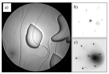
That the islands are indeed composed of carbon in the form of graphene is shown by their characteristic LEED pattern on Ru(0001)MoritzPRL2010 . By inserting an illumination aperture into the incoming electron beam and thus restricting the illuminated area to one such island, the diffraction pattern corresponding to the island’s surface can be recorded, performing in this way Selected Area Diffraction, as shown in Fig. 1b. This is a moiré pattern formed due to the coincidence of the lattices of the graphene overlayer (lattice constant: 0.246 nm) and the Ru(0001) surface (lateral lattice parameter: 0.271 nm). The (11) pattern (Fig. 1c) of the latter can be observed on the clean regions uncovered by the graphene.
Li was deposited onto Ru(0001) surfaces containing epitaxial graphene islands. The work function was continuously monitored during Li dosing. For this purpose, LEEM images were recorded as a function of the start voltage (SV), defined as the potential difference between the cathode and the sample. The SV was swept typically between -3.0 V and 3.0 V repeatedly during Li evaporation. The reflected electron intensity was integrated inside a user-defined window that can be placed either on a graphene island or on the clean Ru(0001) surface. Typical resulting reflectivity vs. SV curves are shown in Fig. 2. Incoming electrons with kinetic energies lower than the sample’s work function cannot penetrate into the solid and are completely reflected at the surface. Therefore, upon lowering the SV, a transition to a nearly complete reflectivity (mirror modeBauerBook2014 ) takes place when the SV equals the difference of work functions of sample and cathode. This transition can be used to monitor the sample’s work function evolution. In this work, its precise value has been taken as the SV at which the derivative of the reflectivity curve attains its maximum absolute value.
Figure 2 displays two sets of reflectivity vs. SV curves recorded during Li deposition: (a) On a graphene island, for a deposition time of 3 h, and (b) on a clean Ru(0001) region, for a deposition time of 1 h 45 min. Although there is in both cases a noticeable decrease of the work function upon Li-deposition, it is clear that the effect is less pronounced in the graphene / Ru system, as will be commented below.
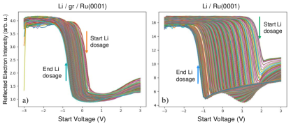
After the completion of each experiment of Li deposition, a new reflectivity curve was recorded in a wider energy range (-5.0 eV - 20.0 eV). One example is shown in Figure 3 with a dashed blue line (corresponding to the experiment of Fig. 2a), together with the corresponding curve on the graphene island before deposition for comparison (dashed black line). The total amount of Li deposited is close to that producing the maximum reduction of the work function in the system, as will be shown below. Data have been normalized to the maximal electron reflected intensity. The decrease of the work function of the graphene island, measured about 5 min after finishing the Li deposition (Fig. 3) amounts to 0.8 eV. One point to be mentioned is that, as deduced from the first and last curves recorded in real time during deposition (Fig. 2), the decrease in work function amounts to 1.0 eV. This means that the work function of the Li/graphene/Ru(0001) system slightly increases in the time following the end of the Li deposition, showing that there is a measurable evolution at room temperature of the Li-covered surface.
The local character of LEEM microscopy allows us to compare with the evolution of the clean Ru(0001) surface upon Li deposition. For this purpose, the corresponding reflectivity curves of the clean and Li-covered Ru(0001) surfaces, after deposition of the same amount of Li, are included in Figure 3 with solid lines. For Ru(0001), the reduction of the work function upon Li deposition amounts to 3.3 eV, close to the maximal reduction in this system, in agreement with published resultsBromberger2002 , compared to the 0.8 eV found for a similar coverage on the epitaxial graphene/Ru(0001) islands (Fig. 3a, dashed lines).
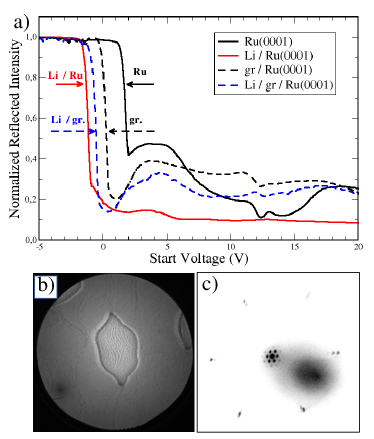
After Li deposition, the typical aspect of the graphene/Ru(0001) islands is shown in Fig. 3b). A somewhat granular structure can be appreciated inside the islands. In addition, they display a LEED pattern, shown in Fig. 3c), with a similar moiré structure as before deposition (Figure 1b), now with higher background intensity. Thus, no new superstructure is formed, either with respect to the substrate Ru(0001) surface or to the graphene overlayer, upon adsorption or incorporation of Li in the graphene islands.
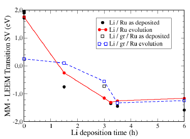
A compilation of results for the evolution of the work function of both the graphene islands and the uncovered Ru(0001) surface as a function of the Li deposition time is shown in Fig. 4. It can be seen that in the case of the Ru(0001) surface, the work function initially decreases rapidly with increasing Li coverage, reaching a maximum reduction of about 3.3 eV for the clean Ru surface (corresponding to a coverage of 0.3 ML-0.5 MLBromberger2002 ). On the other hand, the work function of the graphene/Ru islands decreases initially very slowly and then a more rapid decrease takes place reaching a maximal reduction of about 1.5 eV. This is achieved for a similar coverage as the one which gives the maximal reduction of work function for Li/Ru(0001). For higher Li coverages, the work function evolution shows a slight increase (about 0.2 eV for the clean Ru surface, about 0.1 eV for graphene/Ru as deduced from the measurements performed several minutes after Li deposition). The behavior for Li/Ru(0001) is the canonical one observed for alkali-atom deposition on transition-metal surfaces ZangwillBook . The strong initial decrease is due to the formation of a surface dipole layer as a consequence of the large electron transfer from the highly electronegative alkali atoms to the transition metal. This process reaches its maximum for an alkali coverage of the order of 0.5 ML. For higher coverages a small increase of the work function takes place due to depolarizing effect of neighbour dipoles (ToppingTopping1927 model) and possibly also to a decrease in the electronic polarizability of the charge cloud due to electron transfer VerhoefSS1997 .
An aspect which needs to be addressed is the effect on the measured work functions of the local electric fields arising from the coexistence of regions (patches) of different work functions as the Li coverage increases. At the beginning of deposition, Li atoms are expected to be randomly distributed on the surface, well separated from each other due to the electrostatic repulsion of dipoles. These conditions correspond to the small-patch regime, in which the measured work function gives a surface-averaged value allowing the determination of the induced surface dipoleBundaleski2013 . As coverage increases, condensation of adsorbate islands sets in and thus a coexistence of patches of surface covered by dilute Li atoms and surface covered by condensed Li atoms is expected, the latter with higher work function due to the depolarizing field of nearby dipoles. At some coverage, we must thus enter into the large-patch regime, favoured by the high extraction field produced by the 10 kV applied to the objective lens of the LEEM, of order 104 V/mm. This can be associated with the granular aspect of the graphene islands, as well as the Ru substrate, after Li deposition (Fig. 3b). In this regime the emission or absorption of electrons is dominated by the low work function patches independently of their size, so that the dependence of the measured work function on coverage tends to become weaker and a smooth decrease approaching saturation is expected. These considerations apply to the Li-covered regions both of the Ru(0001) substrate and of the graphene/Ru(0001) islands. The time dependence found in the system, i.e., the increase of work function measured following Li deposition can be ascribed to the rearrangement of Li, favoured by its high mobility, from the dilute-dipole to the compact island phases with a higher work function.
The maximum work function reduction upon Li deposition is a factor of 2 smaller for graphene/Ru than for the clean Ru(0001) surface (1.5 eV vs. 3.3 eV). Considering the electronegativities of the atoms involved (difference in Mulliken’s electronegativity for Li-C is 6.8 eV, compared to 5.4 eV for Li-RuMullikenJCP1934 ; HinzeJACS1962 ), we would expect a higher electron transfer for Li/C than for Li/Ru and therefore, a larger reduction of the work function for the Li/graphene/Ru(0001) surface than for Li/Ru(0001), if Li is residing on the surface of the graphene islands. It could be even larger considering that a charge transfer from the C atoms to the Ru substrate has already taken place, as shown by the work function reduction of gr/Ru(0001) by about 1.6 eV respect to Ru(0001), leaving the graphene surface positively charged. However, the opposite is found. This strongly suggests that the Li atoms are not simply sitting on top of the graphene/Ru(0001) surface. Such would be the situation if the Li atoms were being intercalated at the graphene/Ru interface upon deposition already at room temperature. This is in agreement with calculations indicating that Li cannot reside on the surface of defect-free grapheneLee_Persson2012 ; Dimakis2019 . The picture of Li atoms falling on top of the graphene islands, diffusing to the edges and from there onto the Ru terraces is consistent with the sharp decrease of the work function that takes place only after an appreciable Li coverage; the intercalation would then significantly proceed only after the Ru(0001) terraces have been covered by 0.3 ML - 0.5 ML Li and by a mechanism of diffusion following a concentration gradient across the island edges into the interior of the islands.
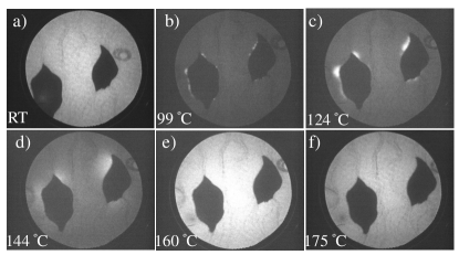
The maximal reduction of the work function of Ru(0001) upon Li adsorption amounts to 3.3 eV. Since the work function of the clean surface is 5.5 eVWandeltSS1981 , the final value, 2.3 eV, is low enough to allow photoemission of electrons by visible light. Illuminating with a violet laser (photon energy: 3.06 eV) and collecting the produced photoelectrons with the image column of the microscope allows us to image the Li-covered Ru(0001) with its graphene islands, performing in this way photoemission electron microscopy (PEEM). Examples of PEEM images of a Li-covered Ru(0001) surface containing two graphene islands can be seen in Figure 5.
A final experiment in PEEM was performed in order to gain insight into the presence of Li in the graphene islands. After deposition of about 0.5 ML of Li, the surface was continuously imaged in PEEM mode while raising the temperature. A selection of images of the process at different temperatures is shown in Figure 5. In the image at 99∘ C (b), small bright spots can be seen in some regions at the edges of the graphene islands (preferentially at the corners) which were not visible in the images at room temperature. As the temperature is raised, these regions first become brighter and then appear to grow, i.e. the regions of higher photoemission yield become wider and spread from the graphene islands away, while their intensity reduces as they expand across the Ru(0001) terraces, until they finally occupy the complete surface uncovered by the graphene islands. This suggests that temperature promotes the flow of Li out of the islands at their edges, mainly at the corner points (and suggests these can be also preferred places for Li intercalation into the islands) and its diffusion onto the Ru terraces, increasing the amount of Li adsorbed there and promoting a further reduction of the work function and an increase in photoelectron intensity. This is a further support for the fact that Li atoms were originally intercalated below the graphene layer following deposition. The Li density there can be higher than on the Ru(0001) surface after deposition because of the higher affinity of Li to C than to Ru, as quantified by the higher electronegativity difference between Li and C. Thermal activation is then likely to promote diffusion of Li out of the graphene islands onto the Ru(0001) terraces following the concentration gradient. This process sets in at temperatures around 100∘ C, from which an activation barrier for Li diffusion of the order of 40 meV can be deduced. This small value is reasonable and explains the time evolution of the work function after finishing Li deposition (see Fig. 4) and the high mobility of Li atoms. It compares also well with the 46 meV calculated for the similar case of Na diffusion on Ru(0001)Raghavan2021 .
IV Conclusions
Summarizing, we have grown submonolayer islands of epitaxial graphene on Ru(0001) and have monitored their morphology, structure and electronic properties (work function) by means of LEEM in real time during Li deposition, comparing with the evolution of the clean Ru(0001) surface. Li reduces the work function of graphene/Ru(0001) by as much as 1.5 eV, significantly less than the 3.3 eV found for Ru(0001). Intercalation takes place at room temperature without forming any new superstructure. This behavior is confirmed by observing the temperature evolution with visible-light PEEM, taking advantage of the work function reduction in the system. Temperature promotes the diffusion of Li atoms out of the graphene islands preferentially at their corners and their expansion onto the Ru(0001) terraces.
V Aknowledgments
This work is supported by grant RTI2018-095303-B-C51, funded by MCIN/AEI/10.13039/501100011033 and by “ERDF A way of making Europe”, by grant PID2020-117024GB-C43 (Ministerio de Ciencia e Innovación) and by grant S2018-NMT-4321, funded by the Regional Government of Madrid and by “ERDF A way of making Europe”. L.M.G. acknowledges a sabbatical grant from DGAPA-UNAM.
References
References
- (1) L. Daukiya et al., Progress in Surface Science 94, 1 (2019).
- (2) R. P. Smith et al., Physica C: Superconductivity and its Applications 514, 50 (2015).
- (3) J. R. Dahn, T. Zheng, Y. Liu, and J. S. Xue, Science 270, 590 (1995).
- (4) J.-M. Tarascon and M. Armand, Nature 414, 359 (2001).
- (5) A. S. Aricò, P. Bruce, B. Scrosati, J.-M. Tarascon, and W. van Schalkwijk, Nature Materials 4, 366 (2005).
- (6) J. Asenbauer et al., Sustainable Energy & Fuels 4, 5387 (2020).
- (7) G. K. Wertheim, P. T. T. M. Van Attekum, and S. Basu, Solid State Communications 33, 1127 (1980).
- (8) W. Eberhardt, I. T. McGovern, E. W. Plummer, and J. E. Fisher, Physical Review Letters 44, 200 (1980).
- (9) T. Fauster, F. J. Himpsel, J. E. Fischer, and E. W. Plummer, Physical Review Letters 51, 430 (1983).
- (10) N. A. W. Holzwarth, S. Rabii, and L. A. Girifalco, Phys. Rev. B 18, 5190 (1978).
- (11) N. A. W. Holzwarth, S. G. Louie, and S. Rabii, Phys. Rev. B 30, 2219 (1984).
- (12) C. Hartwigsen, W. Witschel, and E. Spohr, Phys. Rev. B 55, 4953 (1997).
- (13) G. Csányi, P. B. Littlewood, A. H. Nevidomskyy, C. J. Pickard, and B. D. Simons, Nature Physics 1, 42 (2005).
- (14) G. Radhakrishnan, J. D. Cardema, P. M. Adams, H. I. Kim, and B. Foran, Journal of The Electrochemical Society 159, A752 (2012).
- (15) L. David et al., ACS Applied Materials & Interfaces 5, 546 (2013).
- (16) F. Yao et al., Journal of the American Chemical Society 134, 8646 (2012).
- (17) M. A. Editor, LaptopMag (2014).
- (18) J. Wintterlin and M.-L. Bocquet, Surface Science 603, 1841 (2009).
- (19) C. Virojanadara, S. Watcharinyanon, A. A. Zakharov, and L. I. Johansson, Physical Review B 82, 205402 (2010).
- (20) K. V. Emtsev, A. A. Zakharov, C. Coletti, S. Forti, and U. Starke, Physical Review B 84, 125423 (2011).
- (21) I. Gierz et al., Physical Review B 81, 235408 (2010).
- (22) K. Yagyu et al., Applied Physics Letters 104, 053115 (2014).
- (23) Y. Zhang, H. Zhang, Y. Cai, J. Song, and P. He, Nanotechnology 28, 075701 (2017).
- (24) N. Briggs et al., Nature Materials 19, 637 (2020).
- (25) P. W. Sutter, J.-I. Flege, and E. A. Sutter, Nature Materials 7, 406 (2008).
- (26) K. McCarty, P. Feibelman, E. Loginova, and N. Bartelt, Carbon 47, 1806 (2009).
- (27) Y. Cui, Q. Fu, and X. Bao, Physical Chemistry Chemical Physics 12, 5053 (2010).
- (28) B. Borca et al., New Journal of Physics 12, 093018 (2010).
- (29) L. Huang et al., Applied Physics Letters 99, 163107 (2011).
- (30) S. Ulstrup et al., Surface Science 678, 57 (2018).
- (31) E. Bauer, Surface Microscopy with Low-Energy Electrons (, 2014).
- (32) W. Moritz et al., Physical Review Letters 104, 136102 (2010).
- (33) C. Bromberger, H. Jänsch, and D. Fick, Surface Science 506, 129 (2002).
- (34) A. Zangwill, Physics at Surfaces (, 1988).
- (35) J. Topping, Proc. R. Soc. Lond. 114, 67 (1927).
- (36) R. W. Verhoef and M. Asscher, Surface Science 391, 11 (1997).
- (37) N. Bundaleski, J. Trigueiro, A. Silva, A. Moutinho, and O. Teodoro, Journal of Applied Physics 113, 183720 (2013), https://doi.org/10.1063/1.4804663.
- (38) R. Mulliken, The Journal of Chemical Physics 2, 782 (1934).
- (39) J. Hinze and H. H. Jaffe, Journal of the American Chemical Society 84, 540 (1962).
- (40) E. Lee and K. Persson, Nano Letters 12, 4624 (2012).
- (41) N. Dimakis et al., Molecules 24, 754 (2019).
- (42) K. Wandelt, J. Hulse, and J. Küppers, Surface Science 104, 212 (1981).
- (43) A. Raghavan et al., Phys. Chem. Chem. Phys. 23, 7822 (2021).