Adsorption of water on the pristine and defective semiconducting 2D CrPX3 monolayers (X: S, Se)
Abstract
The effect of vacancy and water adsorption on the electronic structure of semiconducting 2D trichalcogenide material CrPX3 (X: S, Se) is studied using state-of-the-art density functional theory (DFT) approach. It is found that chalcogen vacancies play a minor role on the electronic structure of CrPX3 in the vicinity of the Fermi level leading to the slightly reduced band gap for these materials, however, inducing strongly localised defect states which are placed in the energy gap formed by the valence band states. Our DFT calculations show that the interaction of water molecules with CrPX3, pristine and defective, can be described as physisorption and the adsorption energy for H2O is insensitive to the difference between pristine and chalcogen-defective surface of trichalcogenide material. These results are the first steps for the theoretical description of the ambient molecules interaction with 2D semiconducting CrPX3 material, that is important for its future experimental studies and possible applications.
1 Introduction
The class of the pure 2D and quasi-2D materials is rapidly developing [1, 2, 3, 4] regularly bringing new exciting phenomena, like observation of the 2D magnetic order [5, 6, 7], superconductivity [8, 9], and exciting optical properties [10, 11]. Among these materials, quasi-2D transition metal trichalcogenides (MPX3, M: transition metal, X: S, Se) recently attracted increased attention because of their possible applications in many areas. It was proposed that they can be used as low-dimensional spin-polarised conductors which spin character can be tuned by the applied bias [12], in photocatalysis for the efficient water splitting and hydrogen production [13, 14, 15], as efficient materials for the Li storage [16], and, for example, the tuning of the vacancy state can lead to the low-dimensional ferromagnetic state [17].
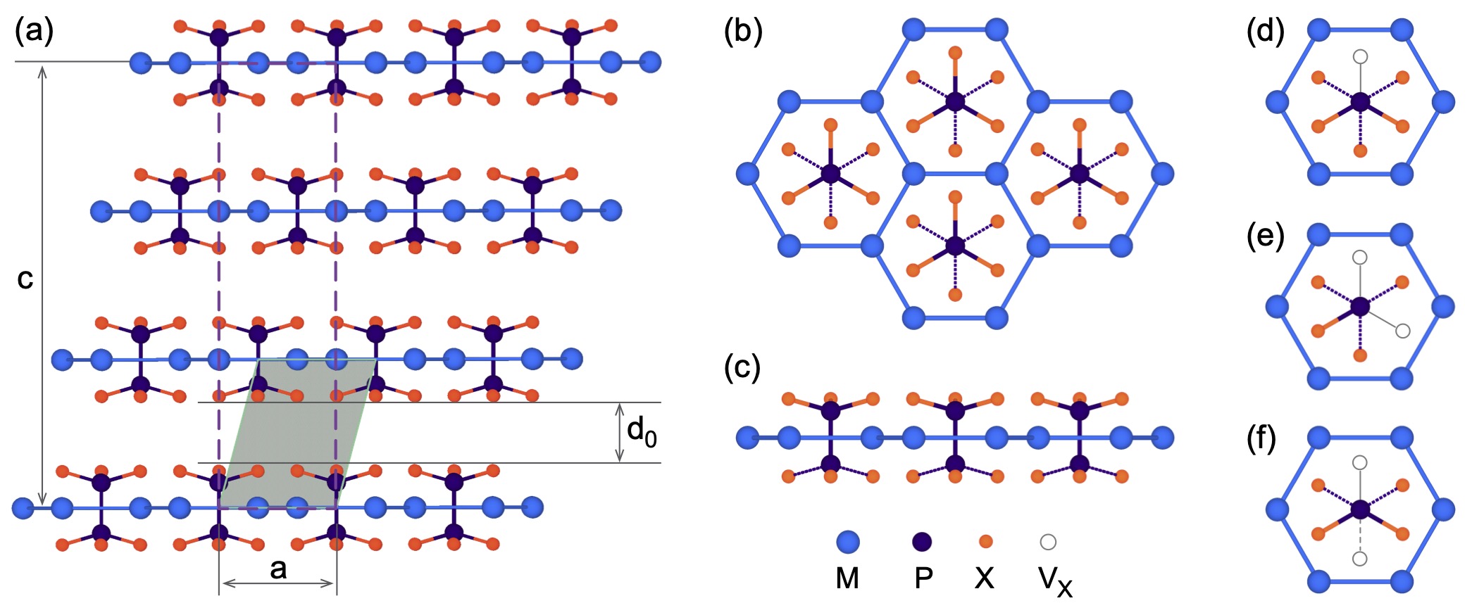
From the crystallographic point of view, these materials are similar to, e. g., MoS2, where one third of the metal atoms is substituted by P–P dimers and in this case the metal layer in MPX3 is encapsulated by both chalcogens and phosphorus atoms (Fig. 1). Diversity in transition metals and two different chalcogens can lead to a wide variation in the electronic and magnetic properties of these materials. Also, the simultaneous presence of sulphur and phosphorus in these compounds can cause a synergetic effect on the electronic structure of the central metal atoms. Moreover, due to the layered structure of MPX3, they can be easily prepared as two-dimensional nanostructures having a large surface area with large number of active sites. Surprisingly, the electronic structure of these materials is mainly addressed only from the theory side and the experimental studies are very rear and sporadically appear in the literature [18], moreover not always correctly interpreting the obtained experimental data [19, 20]. Also, the influence of vacancies as well as ambient adsorbates on the magnetic and electronic properties of MPX3 are not studied at all.
Here, we present state-of-the-art density functional theory (DFT) studies of Cr-based phosphorus trichalcogenides (CrPS3 and CrPSe3). These materials were recently synthesised and studied with respect to their electrochemical sensing and energy applications [20]. In our work we address many aspects of these materials, like stability, chalcogen defects formation and adsorption of water molecules on pristine and defective 2D CrPX3 layer. We found that in all cases, the electronic structure around the top of the valence band of CrPX3 remains insensitive and main modifications are connected with the valence states redistributions at large binding energies. These results demonstrate that CrPX3 are robust to the external factors, like chalcogen defects formation and ambient molecules adsorption, that can be utilised in future applications of these materials as, e. g., protective coatings or inert barriers for molecules.
2 Computational details
Spin-polarised DFT calculations based on plane-wave basis sets of eV cutoff energy were performed with the Vienna ab initio simulation package (VASP). [21, 22, 23] The Perdew-Burke-Ernzerhof (PBE) exchange-correlation functional [24] was employed. The electron-ion interaction was described within the projector augmented wave (PAW) method [25] with Cr (, , ), P (, ), S (, ) and Se (, ) states treated as valence states. The Brillouin-zone integration was performed on -centred symmetry reduced Monkhorst-Pack meshes using a Gaussian smearing with eV, except for the calculation of total energies. For these calculations, the tetrahedron method with Blöchl corrections [26] was employed. The and -meshes were used for the studies of bulk and monolayer CrPX3, respectively, and the -mesh was used for the () supercells consisting of -fold unit monolayers. The DFT+ scheme [27, 28] was adopted for the treatment of Cr orbitals, with the parameter equal to eV. Dispersion interactions were considered adding a atom-atom term as parameterised by Grimme (“D2” parameterisation) [29]. This approach yields structural parameters, which are in good agreement with available experimental data [20].
When modelling CrPX3 monolayers, the lattice constant in the lateral plane was set according to the optimised lattice constant of bulk CrPX3. A vacuum gap was set to approximately Å. During structure optimisation, the convergence criteria for energy and force were set equal to eV and eV/Å, respectively.
The cleavage energy was calculated as
where is the van der Waals gap of bulk crystal and is the in-plane area.
To extract the exchange interaction parameters between Cr ions spins, the Heisenberg Hamiltonian was considered
where is the net spin magnetic moment of the Cr ions at site , three different distance magnetic coupling parameters were estimated, considering one central Cr ions interacted with three nearest neighbouring (NN, ), six next-nearest neighbouring (2NN, ), and three third-nearest neighbouring (3NN, ) Cr ions, respectively. Here, the long-range magnetic exchange parameters () can be obtained as [30]
| (1) | |||
where is the calculated magnetic moment of the Cr ion and , , , are the total energies in ferromagnetic, Néel antiferromagnetic, zigzag antiferromagnetic, and stripy antiferromagnetic configurations, respectively.
To estimate temperature, Monte Carlo simulations were performed within the Metropolis algorithm with periodic boundary conditions [31]. The three exchange parameters , and were used in a superlattice containing a large enough amount of magnetic sites to accurately evaluate the value. Upon the heat capacity reaching the equilibrium state at a given temperature, the value can be extracted from the peak of the specific heat profile.
The electrically neutral vacancies were created by removing one or two X atoms from the () supercells. Thereby, the distance between repeated vacancies in the nearest-neighbour cells is larger than Å. The defect formation energy is defined as follows
where is a number of defects, and are the energies of the 2D CrPX3 with and without vacancy, respectively, is the chemical potential of X atom ( eV and eV).
To study the adsorption of a single molecule, a () supercell was used with one water molecule added. Adsorption energies were calculated as
where and are he energies of the isolated 2D CrPX3 and an adsorbate, and is the energy of their interacting assembly.
3 Results and Discussion
3.1 3D CrPX3 (X = S, Se)
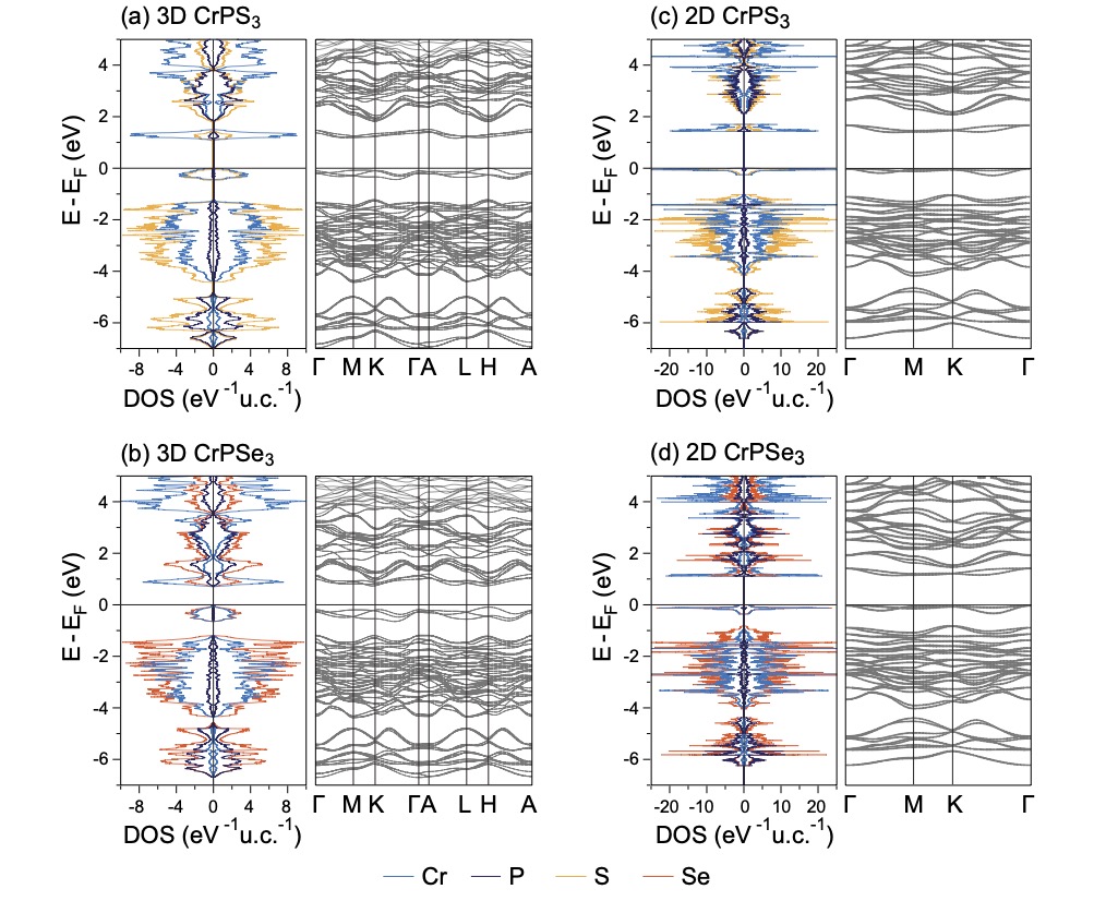
3D bulk MPX3 crystals usually adopt either an stacking in space group space or stacking in space group. Both of them can be represented in hexagonal unit cells (Fig. 1 a). Then every unit cell contains three MPX3 single layers which have symmetry (see Fig. 1 b,c), which are stacked in a different way. Each single-layer are held together by van der Waals forces. The lattice parameters of hexagonal 3D CrPX3 were fully relaxed in nonmagnetic (NM), ferromagnetic (FM) and Néel antiferromagnetic (nAFM) states and they are listed in Table 1 with the respective total energies. Thus, both CrPX3 (X = S, Se) prefer the symmetry, that is in agreement with available experimental data [32]. For both CrPS3 and CrPSe3, the energetically most favourable structure corresponds to the nAFM configuration (Tab. 1). The band structure and density of states (DOS) calculated for the ground-state structures of 3D CrPS3 and CrPSe3 are shown in Figure 2 (a) and (b), respectively. From these results one can see, that the both systems under study are indirect band gaps semiconductors. The band gaps obtained by the PBE method are eV for bulk CrPS3 and eV for bulk CrPSe3. The upper valence bands (VBs) are mainly formed by S/Se and equal to that by the Cr orbitals; the lower conduction bands (CBs) are composed of Cr states with somewhat contribution from S/Se . The partial contributions from P orbitals are very small in VBs as well as CBs. These results are very different from the respective data known for MnPX3 [33] and NiPX3 [18, 34], where the contribution of metal states in VBs was insignificant.
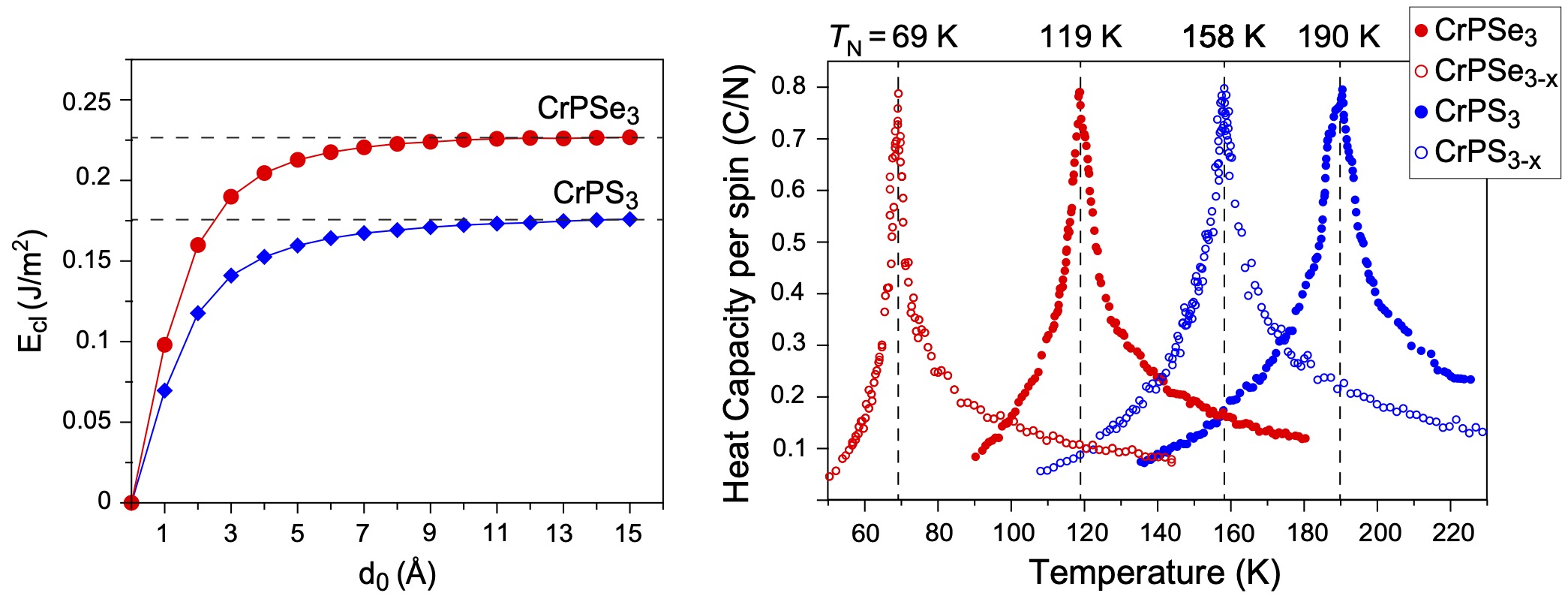
It is expected that individual CrPX3 layers can be isolated by mechanical exfoliation. In this regard, the cleavage energy () of a layered material is an essential property that need to be considered. The calculated values, J m-2 and J m-2 (Fig. 3, left panel), are smaller than that of a bulk graphite ( J m-2) [35], which is used as an indicator for the feasibility of exfoliation of materials in experiments. The obtained values are in the same range as recently published for MnPX3 and NiPX3 [33, 34].
3.2 2D CrPX3 (X = S, Se) monolayers
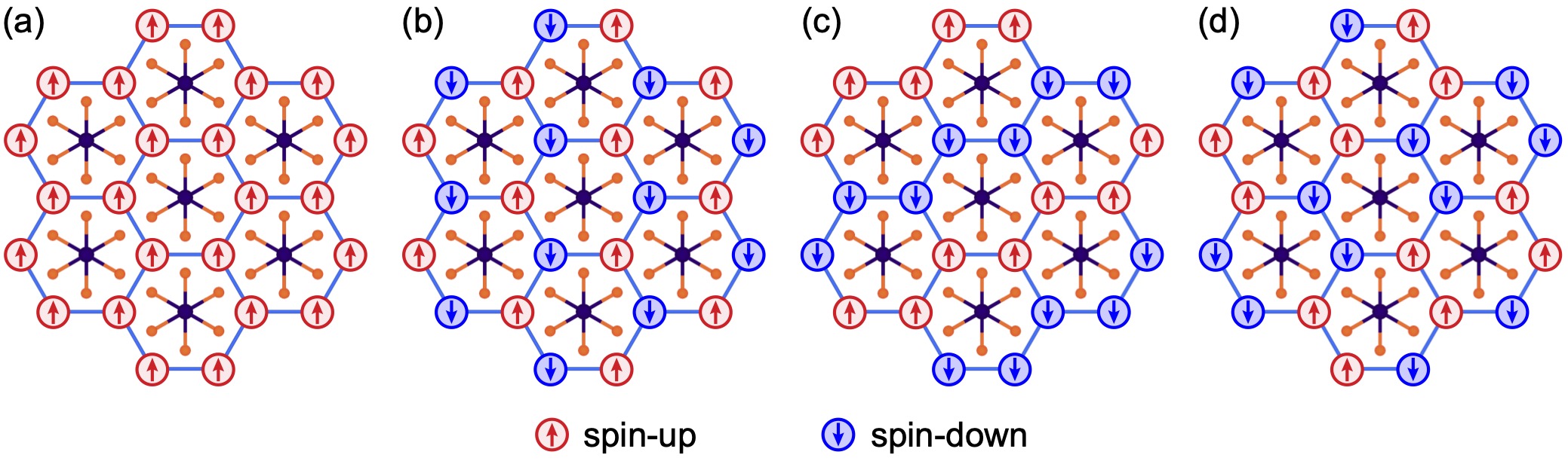
Four possible magnetic configurations were investigated to evaluate the ground state of 2D CrPX3 monolayers: The mentioned above FM (Fig. 4 a), and nAFM (Fig. 4 b) were supplemented by a zig-zag AFM (zAFM, Fig. 4 c) and a stripy AFM (sAFM, Fig. 4 d). The obtained results are listed in Table 2. It can be seen that the lowest energy configurations for the 2D CrPX3 (X = S, Se) monolayers are the Néel AFM states.
The 2D CrPS3 and CrPSe3 in their ground states keep an indirect semiconductor behaviour (Fig. 2c,d). Due to the quantum confinement effects, the band gaps are slightly larger than the values calculated for the bulk phases and are eV and eV for the 2D CrPS3 and CrPSe3, respectively. As for the bulk materials, the bands in the vicinity of Fermi energy are mostly composed of Cr- and S/Se- orbitals.
The exchange-coupling parameters (, , ) describing the magnetic interactions between Cr2+ ions were calculated according to eqn. (LABEL:equ:J) and are listed in Tab. 2. According to the Goodenough-Kanamori-Anderson (GKA) rules [36, 37], the origin of the nAFM ground state can be attributed to the competition between the NN AFM direct Cr–Cr () exchange interactions and the indirect Cr–SeSe–Cr () superexchange interactions [38]. The calculated parameters were used in the Monte-Carlo simulations of Néel temperatures of CrPX3 monolayers. The estimated is K for 2D CrPS3 and K for 2D CrPSe3 (Fig. 3, right panel). These results are in very good agreement with the experimental result available for CrPSe3, that is: K [20].
3.3 Chalcogen defects
Mechanical exfoliation used for monolayers production, can lead to formation of chalcogen vacancies. Therefore, we consider three different kinds of defects: (i) one vacancy at X-site, named as VX@1L with a defect concentration about % (Fig. 1 c); (ii) two vacancies at the neighbouring X-sites of the same chalcogen sublayer named as VX2@1L with a concentration about % (Fig. 1 d); (iii) two vacancies at X-sites of the different chalcogen sub-layers named as VX2@2L with a concentration about % (Fig. 1 e). The defect formation energies (Tab. 3) are of the same order that is known for the other MPX3 family members [33, 34] and are rather low in all cases presumably indicating a feasibility of formation of these kinds of defects in experiments. According to the defect formation energies, it is found that VX@1L defects are the most favourable to form, followed by V2X@2L and V2X@1L. Also, we can observed that for the same defect type, Se vacancy is more likely to occur than S vacancy, which correlates with the respective electronegativity values. Although the rather low obtained for all considered cases, we expect that in experimental conditions the formation of single chalcogen defects is more feasible and from now on we will focus on detailed consideration of VX@1L.
Removal of chalcogen atom leads to some modifications of the local lattice and electronic structures. As compared to the pristine CrPX3 monolayer, the phosphorous dimers tend to moving closer to the vacancy. The angle, which P–P dimer forms with the vertical direction is and for X = S and Se, respectively. The dimer is pulled out from a monolayer. This leads to somewhat increase of the P–S bond length (by Å), while the P–P bond lengths remain basically unchanged.
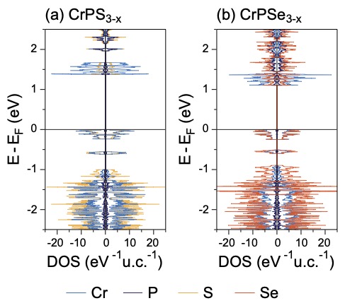
The electrons left behind upon removal of a chalcogen atom, occupy the easily available electronic states of a (P2X5) entity. The magnetic moments of the Cr2+-ions nearby the vacancy are coupled antiferromagnetically. Similarly to the data recently published for MnPX3 [33], there are no well-localised defect state generated within the band gap in the DOS (Fig. 5). As a result, the energy gap width of the defective monolayers stays almost unchanged regarding the pristine CrPX3: eV and eV for the defective CrPS3 and CrPSe3, respectively. At the same time, at eV a new state appears, which is formed by S/Se and equal to that by the Cr orbitals.
The estimated value for the defective trichalcogenide monolayers is reduced to K and K for CrPS3 and CrPSe3, respectively (Fig. 3). This effect is generally expected because the X-vacancy formation leads to the drastic reduction of the exchange-coupling parameters ( meV, meV, meV for CrPS3-x; meV, meV, meV for CrPSe3-x). At the same time the strongly localised magnetic moments of Cr2+ ions remain the same.
3.4 Adsorption of H2O
The effect of adsorption of molecular water plays an important role in various applications and technological processes, since they are present in the environment of any device. Thus in the next step we investigate how adsorption of H2O affects the electronic properties of CrPX3 monolayers.
Various high-symmetry adsorption sites and adsorption orientations are taken into account. Considering the pristine monolayers, all adsorption configurations have similar adsorption energies which range from meV to meV and from meV to meV for 2D CrPS3 and 2D CrPSe3, respectively. In the relaxed structures water stays almost parallel to the substrate and the vertical distance between the molecule and the CrPX3 monolayer is always above Å.
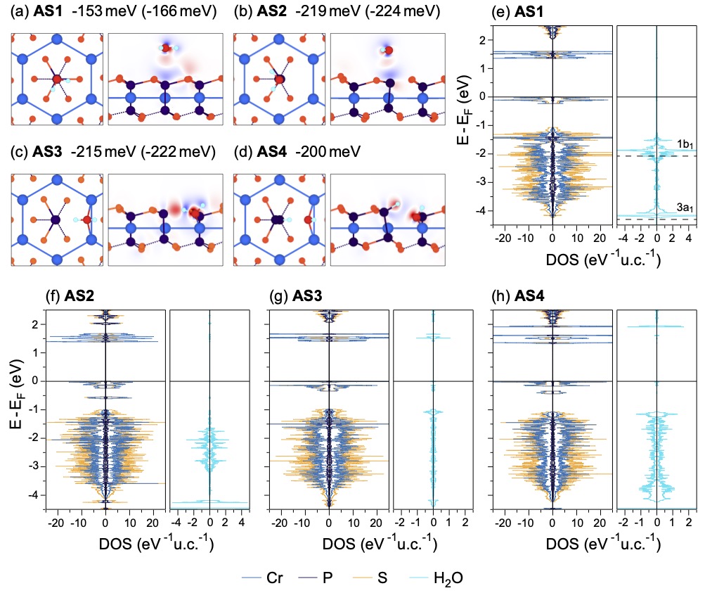
For pristine monolayers, in the most stable adsorption structure (AS1, Fig. 6a), a water molecule attaches with its oxygen atom to an P atom [ Å and Å for CrPS3 and CrPSe3, respectively] and the H atoms are directed towards the neighbouring X atoms. In accordance with the weak interaction, the structural parameters of H2O as well as of the studied monolayer undergo insignificant changes. As follows from the electron density redistribution plot (Fig. 6a), upon adsorption the main charge rearrangement takes place between O and P atoms. Charge accumulation in the -orbital of P on the side of the adsorbate indicates that it is the main orbital participating in the bonding. This charge accumulation is accompanied with a depletion at the hydrogen positions. These observation are in line with the effects arising in DOS due to the interaction between H2O and CrPX3 (Fig. 6e): Hybridisation between states of P and the water lone pair [ molecular orbital (MO) of H2O] takes place, that results in broadening of the respective water derived states. Besides, a slight upward shift with respect to the MO of gas phase water molecule is observed. The obtained results on the adsorption of H2O on pristine CrPX3 are in general trend observed for graphene and for the other 2D chalcogenides. The adsorption energies for H2O on graphene, MoS2, and WS2 are eV, eV, and eV, respectively [39, 40, 41], indicating the physisorption nature of interaction.
Considering the defective monolayers, the situation is more interesting. Firstly, the adsorption structure similar to AS1 exists. It is abbreviated as AS2 and presented in Figure 6b. In this case, the interaction between H2O and the substate is stronger ( meV and meV), which is reflected by the reduced distance Å and Å for CrPS3 and CrPSe3, respectively. In the rest, the electronic structures of the molecule and substate undergo qualitatively similar changes as in the case of AS1 (Fig. 6f).
In addition to AS2, a structure, called AS3 was investigated, where water molecule is coordinated between two Cr ions as it is shown in Figure 6c. (Similar configuration was found to be the energetically most favourable when studying water adsorption on NiPX3-x [34]). Charge accumulation is observed between O and two Cr atoms as well as between H and P atom, which lost the chalcogen neighbour (Fig. 6c). Significant contribution of the the and MOs to the bonding with the monolayer is expressed in their substantial broadening due to hybridisation with P- sates. The healing of vacancy is accompanied by shift of the the defect derived state from its original position to lower binding energies where it is mixed with the valence band states.
The interaction between between H and P atoms in AS3 has one important effects on the geometric structure: A significant elongation of the H–O bond from Å for the gas-phase molecule to Å and Å for the adsorbed molecule on CrPS3-x and CrPSe3-x, respectively. A further H–O bond elongation up to Å leads to structure AS4 (Fig. 6d), which is slightly higher in energy as compared to AS3. Here the P–H bond is formed ( Å). Similarly to recently published results for NiPX3 [34], the corresponding structure was found to be unstable for CrPSe3-x. The weaker adsorbate-substrate interaction in the case of AS4 is reflected by less pronounced changes in the DOS of the interacting species. By that the qualitative tendency of the induced modifications in AS4 is similar to AS3.
4 Conclusions
In conclusions, we performed systematic DFT studies of pristine and chalcogen-defective 2D CrPX3 (X: S, Se). It is shown that both pristine materials are wide gap semiconductors in the ground state with a band gap of eV and eV, respectively. The chalcogen vacancies are characterised by very strongly localised defect states located at eV below the valence band maximum and in the gap formed by valence band states, indicating the minimal influence of such defects on the optical and transport properties of CrPX3. The adsorption of H2O on the pristine and chalcogen-defective 2D CrPX3 layers is always described as a physisorption, with possible water splitting. However, the clear preferential adsorption of H2O on all kinds of surfaces of CrPX3, molecular or dissociative, is not observed. It is found that in all cases of the surface modifications (chalcogen vacancies or ambient molecules adsorption), the electronic structure of CrPX3 remains robust against these factors, indicating the possible application of these materials as effective protecting coatings.
References
- [1] Zeng M, Xiao Y, Liu J, Yang K and Fu L 2018 Chem Rev 118 6236–6296
- [2] Akinwande D, Huyghebaert C, Wang C H, Serna M I, Goossens S, Li L J, Wong H S P and Koppens F H L 2019 Nature 573 507–518
- [3] Dedkov Y S and Voloshina E 2020 Nanoscale 12 11416–11426
- [4] Andrei E Y and MacDonald A H 2020 Nat. Mater. 1265–1275
- [5] Lee J U, Lee S, Ryoo J H, Kang S, Kim T Y, Kim P, Park C H, Park J G and Cheong H 2016 Nano Lett. 16 7433–7438
- [6] Wang X, Du K, Liu Y Y F, Hu P, Zhang J, Zhang Q, Owen M H S, Lu X, Gan C K, Sengupta P, Kloc C and Xiong Q 2016 2D Mater. 3 031009
- [7] Gong C, Li L, Li Z, Ji H, Stern A, Xia Y, Cao T, Bao W, Wang C, Wang Y, Qiu Z Q, Cava R J, Louie S G, Xia J and Zhang X 2017 Nature 546 265–269
- [8] Cao Y, Fatemi V, Fang S, Watanabe K, Taniguchi T, Kaxiras E and Jarillo-Herrero P 2018 Nature 556 43–50
- [9] Cao Y, Fatemi V, Demir A, Fang S, Tomarken S L, Luo J Y, Sanchez-Yamagishi J D, Watanabe K, Taniguchi T, Kaxiras E, Ashoori R C and Jarillo-Herrero P 2018 Nature 556 80–84
- [10] Kang S, Kim K, Kim B H, Kim J, Sim K I, Lee J U, Lee S, Park K, Yun S, Kim T, Nag A, Walters A, Garcia-Fernandez M, Li J, Chapon L, Zhou K J, Son Y W, Kim J H, Cheong H and Park J G 2020 Nature 583 785–789
- [11] Ma Q, Ren G, Xu K and Ou J Z 2021 Adv. Opt. Mater 9 2001313
- [12] Li X, Wu X and Yang J 2014 J. Am. Chem. Soc. 136 11065–11069
- [13] Cheng Z, Shifa T A, Wang F, Gao Y, He P, Zhang K, Jiang C, Liu Q and He J 2018 Adv. Mater. 30 1707433
- [14] Cheng Z, Sendeku M G and Liu Q 2020 Nanotechnology 31 135405
- [15] Du C F, Liang Q, Dangol R, Zhao J, Ren H, Madhavi S and Yan Q 2018 Nano-Micro Lett. 10 67
- [16] Fan C Y, Zhang X H, Shi Y H, Xu H Y, Zhang J P and Wu X L 2019 J. Mater. Chem. A 7 1529–1538
- [17] Bai W, Hu Z, Xiao C, Guo J, Li Z, Zou Y, Liu X, Zhao J, Tong W, Yan W, Qu Z, Ye B and Xie Y 2020 J. Am. Chem. Soc. 142 10849–10855
- [18] Yan M, Jin Y, Wu Z, Tsaturyan A, Makarova A, Smirnov D, Voloshina E and Dedkov Y 2021 J. Phys. Chem. Lett. 12 2400–2405
- [19] Dedkov Y S, Yan M and Voloshina E 2020 Chem. Phys. Lett. 754 137627
- [20] Gusmão R, Sofer Z, Sedmidubský D, Huber Š and Pumera M 2017 ACS Catal. 7 8159–8170
- [21] Kresse G and Furthmuller J 1996 Comp. Mater. Sci. 6 15–50
- [22] Kresse G and Hafner J 1994 J. Phys.: Condens. Matter 6 8245–8257
- [23] Kresse G and Hafner J 1993 Phys. Rev. B 47 558–561
- [24] Perdew J P, Burke K and Ernzerhof M 1996 Phys. Rev. Lett. 77 3865–3868
- [25] Blöchl P E 1994 Phys. Rev. B 50 17953–17979
- [26] Blöchl P E, Jepsen O and Andersen O K 1994 Phys. Rev. B 49 16223–16233
- [27] Anisimov V I, Aryasetiawan F and Lichtenstein A I 1997 J. Phys.: Condens. Matter 9 767–808
- [28] Dudarev S L, Botton G A, Savrasov S Y, Humphreys C J and Sutton A P 1998 Phys. Rev. B 57 1505–1509
- [29] Grimme S 2006 J. Comput. Chem. 27 1787–1799
- [30] Sivadas N, Daniels M W, Swendsen R H, Okamoto S and Xiao D 2015 Phys. Rev. B 91 235425
- [31] Metropolis N, Rosenbluth A W, Rosenbluth M N, Teller A H and Teller E 1953 J. Chem. Phys. 21 1087–1092
- [32] Brec R, Ouvard G, Louisy A and Rouxel J 1980 Ann. Chim. 5 499–512
- [33] Yang J, Zhou Y, Guo Q, Dedkov Y S and Voloshina E 2020 RSC Adv. 10 851–864
- [34] Wu Z, Xu S, Zhou Y, Guo Q, Dedkov Y and Voloshina E (submitted)
- [35] Zacharia R, Ulbricht H and Hertel T 2004 Phys. Rev. B 69 155406
- [36] Goodenough J B 1955 Phys. Rev. B 100 564–573
- [37] Kanamori J 1960 J. Appl. Phys. 31 S14–S23
- [38] Yang J, Zhou Y, Dedkov Y S and Voloshina E 2020 Adv. Theory Simul. 3 2000228
- [39] Voloshina E, Usvyat D, Schütz M, Dedkov Y and Paulus B 2011 Phys. Chem. Chem. Phys. 13 12041–12047
- [40] Levita G, Restuccia P and Righi M C 2016 Carbon 107 878–884
- [41] Bui V Q, Pham T-T, Le D A, Thi C M and Le H M 2015 J. Phys.: Condens. Matter 27 305005
| X | Symmetry | Magnetic state | ||||
|---|---|---|---|---|---|---|
| S | NM | |||||
| FM | ||||||
| nAFM | ||||||
| NM | ||||||
| FM | ||||||
| nAFM | ||||||
| Se | NM | |||||
| FM | ||||||
| nAFM | ||||||
| NM | ||||||
| FM | ||||||
| nAFM |
| X | Magn. state | ||||||||
|---|---|---|---|---|---|---|---|---|---|
| S | FM | ||||||||
| nAFM | |||||||||
| sAFM | |||||||||
| zAFM | |||||||||
| Se | FM | ||||||||
| nAFM | |||||||||
| sAFM | |||||||||
| zAFM |
| Defect type | X = S | X = Se |
|---|---|---|
| VX@1L | ||
| VX2@1L | ||
| VX2@2L |