Challenges to magnetic doping of thin films of the Dirac semimetal Cd3As2
Abstract
Magnetic doping of topological quantum materials provides an attractive route for studying the effects of time-reversal symmetry breaking. Thus motivated, we explore the introduction of the transition metal Mn into thin films of the Dirac semimetal Cd3As2 during growth by molecular beam epitaxy. Scanning transmission electron microscopy measurements show the formation of a Mn-rich phase at the top surface of Mn-doped Cd3As2 thin films grown using both uniform doping and delta doping. This suggests that Mn acts as a surfactant during epitaxial growth of Cd3As2, resulting in phase separation. Magnetometry measurements of such samples indicate a ferromagnetic phase with out-of-plane magnetic anisotropy. Electrical magneto-transport measurements of these films as a function of temperature, magnetic field, and chemical potential reveal a lower carrier density and higher electron mobility compared to pristine Cd3As2 films grown under similar conditions. This suggests that the surfactant effect might also serve to getter impurities. We observe robust quantum transport (Shubnikov-de Haas oscillations and an incipient integer quantum Hall effect) in very thin (7 nm) Cd3As2 films despite being in direct contact with a structurally disordered surface ferromagnetic overlayer.
I Introduction
Magnetic doping of quantum materials such as semiconductors and topological insulators (TIs) is a well established route to the discovery of interesting emergent quantum phenomena.[1, 2, 3, 4, 5] Magnetically-doped semiconductors such as (Ga,Mn)As have provided an important platform for proof-of-concept spintronic devices [6] while magnetic doping of certain TIs has led to the discovery of the quantum anomalous Hall effect [7, 8, 9]. In the latter case, the key physics is driven by the breaking of time-reversal symmetry by ferromagnetic order induced by the exchange interaction between transition metal dopants (Cr, V, Mn, and Fe) and the extended band states of the TI in the (Bi,Sb)2(Te,Se)3 family.
The success of transition metal doping of semiconductors and TIs provides a strong motivation for exploring similar magnetic doping of other topological materials such as topological Dirac semimetals [10, 11, 12, 13, 14, 15]. Topological Dirac semimetals host three-dimensional Dirac fermions and can be identified as a parent phase of other topological phases, for instance, Weyl semimetals [16, 17]. Introducing magnetic dopants into a Dirac semimetal to break the time-reversal symmetry could lead to the degenerate Dirac fermions separating into two (or four) Weyl fermions and a Weyl semimetal phase [19].
In the last decade, Cd3As2 has been theoretically predicted [18] and experimentally demonstrated [12, 13, 14]as a Dirac semimetal. More recently, high-quality Cd3As2 thin films have been successfully grown using molecular beam epitaxy (MBE) [20, 21, 22, 23] and exhibit the quantum Hall effect [24, 21, 25]. The past success of MBE growth of magnetically-doped semiconductors provides a strong motivation to explore magnetic doping of MBE-grown Cd3As2 thin films as a route toward breaking time-reversal symmetry [19] for realizing novel topological phases such as magnetic Weyl semimetals [26, 27, 28] and monopole superconductors [29]. We are aware of only two published reports on magnetic doping of Cd3As2 thin films using Cr [30] and Mn [31]. These studies principally relied on electrical magneto-resistance measurements to draw conclusions about the effect of magnetic dopants on the Dirac semimetal states and assumed that the magnetic dopants were homogeneously distributed throughout the Cd3As2 film.
In this paper, we describe our attempts to use MBE to dope Mn into the Dirac semimetal Cd3As2. We present a systematic structural and magnetic study of heterostructures using high-angle annular dark-field scanning transmission electron microscopy (HAADF-STEM), energy dispersive X-ray spectroscopy (EDX), atomic force microscopy (AFM), high-resolution x-ray diffraction (XRD), superconducting quantum interference device (SQUID) magnetometry, and electrical transport. We find that instead of being incorporated into the Cd3As2 lattice, the Mn dopants form a Mn-rich layer on the top of the Cd3As2 layer. The Mn-rich layer shows insulating behavior and lowers the carrier density in the Cd3As2 layer underneath. Remarkably, even though the Mn-rich phase/Cd3As2 heterostructure exhibits ferromagnetism at room temperature with out-of-plane anisotropy, the samples show pronounced quantum oscillations and an incipient integer quantum Hall effect at low temperature.
II Results and discussion
The Mn-doped Cd3As2 thin films were grown by MBE in a Veeco EPI 930 chamber. We used epi-ready miscut semi-insulating GaAs (111)B substrates ( toward ). Elemental source materials were evaporated from standard effusion cells containing As (99.999995%), Ga(99.99999%), Sb(99.9999%), Cd (99.9999%), and Mn (99.9998%). The epi-ready GaAs substrates were first annealed inside the MBE chamber to flash off the native oxide at a thermocouple temperature of 720 ∘C (the actual temperature is likely 580 ∘C). Then, we deposited a thin (nm) GaAs layer at the same substrate temperature to smooth the surface. Subsequently, the substrates were cooled down to C under As4 flux for the growth of the GaSb buffer layer with an Sb/Ga beam equivalent pressure (BEP) ratio of 7. We note that the both the GaAs and GaSb layers are highly insulating, as confirmed by control measurements. The substrates were then cooled down to 400 ∘C under Sb4 flux, and further cooled down to 180 ∘C after closing the Sb shutter for the growth of Mn-doped Cd3As2. Once the sample temperature was stable at 180 ∘C, we used the Cd, As, and Mn effusion cells with BEP of Cd around Torr, As around Torr and Mn around Torr.
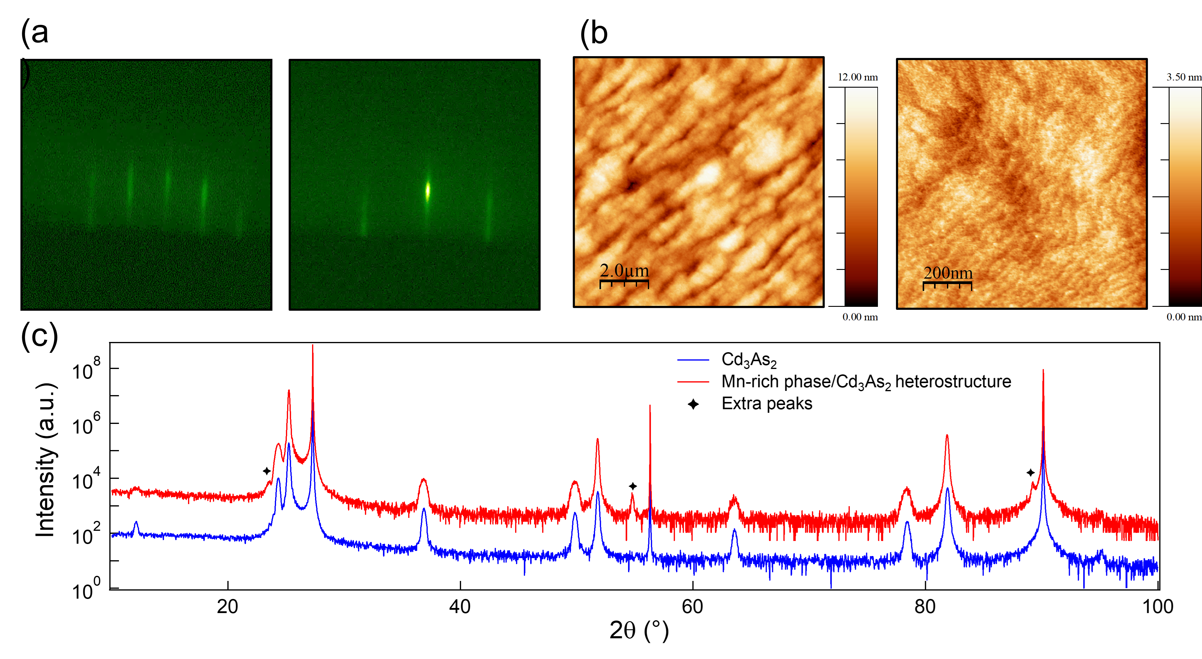
We attempted to grow Mn-doped Cd3As2 thin films using two methods: uniform doping wherein the Mn flux is constant during the growth of Cd3As2 and the delta doping method wherein we interrupt the growth of Cd3As2 and deposit a fractional monolayer of MnAs. The latter approach has been effective in magnetic doping of II-VI and III-V semiconductors [32, 33]. Both growth methods resulted in films with similar characteristics. Reflection high-energy electron diffraction (RHEED) measurements during the growth showed streaky patterns in either approach, indicating a relatively flat surface with some disorder even when depositing a Mn-rich layer (Fig. 1(a). Post-growth, we carried out ex situ AFM measurements (Fig. 1(b)) that indicated a root mean square surface roughness of 1.77 nm over an area of . The steps in the AFM image are due to the miscut substrate; these help prevent twinning defects and improve the quality of the sample. The m2 AFM image in Fig. 1(b) shows the atomic steps of the heterostructure, indicative of the epitaxial growth of the heterostructure. Figure 1(c) compares the XRD scan of a nominally uniformly Mn-doped Cd3As2 film of nomila 25 nm thickness; the plot compares this XRD scan with that of a pristine Cd3As2 film. We observe extra diffraction peaks in the Mn-doped film suggesting the presence of an extra phase. However, from the XRD scan alone, we are unable to identify the crystal structure of this phase.
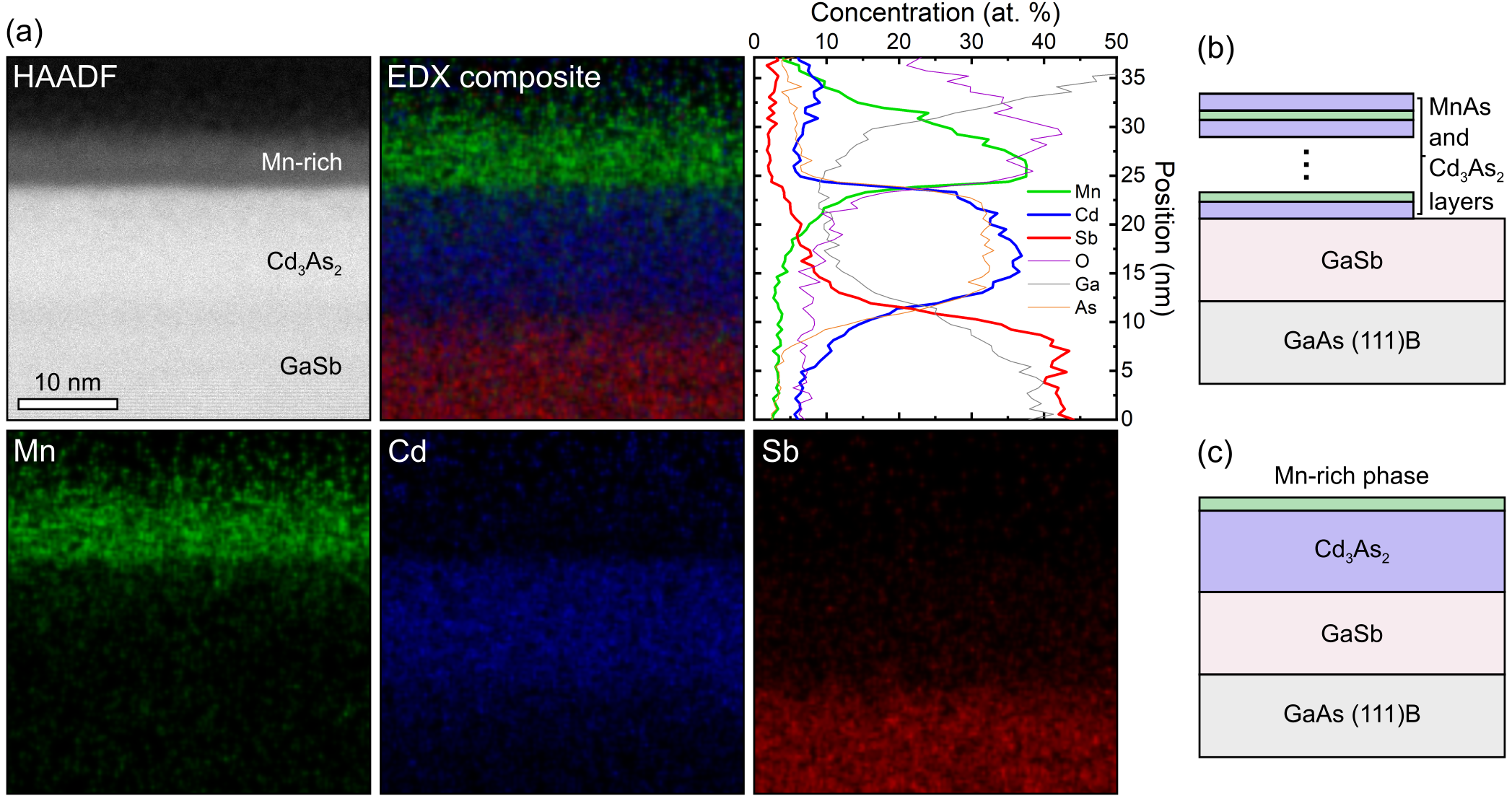
To understand the crystalline structure and elemental distribution within the heterostructures, we used cross-sectional HAADF-STEM imaging and STEM-EDX elemental mapping. We prepared TEM lamella for STEM analysis on a FEI Helios Nanolab G4 dual-beam Focused Ion Beam (FIB). Amorphous carbon was first deposited on the films to protect the surface from damage due to exposure to the ion beam. STEM imaging and EDX spectroscopy were performed on an aberration–corrected FEI Titan G2 60-300 (S)TEM microscope equipped with a CEOS DCOR probe corrector and a super-X EDX spectrometer. The microscope was operated at 300 keV. We acquired HAADF-STEM images with a probe convergence semi-angle of 25.5 mrad and detector inner and outer collection angles of 55 and 200 mrad respectively. We now discuss the TEM measurements obtained from a uniformly Mn-doped Cd3As2 film of nominal 15 nm thickness. Measurements taken on a delta-doped film of similar thickness yield qualitatively similar results (see Supplementary Material at xxx).
High magnification HAADF-STEM images of the film cross-section revealed a crystalline Mn-Cd3As2 film of thickness nm, epitaxial to the GaSb substrate (Fig. 2(a)). A uniform amorphous-like layer ( nm thick) of darker contrast is seen on top of the film. STEM-EDX elemental mapping, shown in Fig. 2(a), was used to obtain compositional information from the heterostructure. Surprisingly, instead of incorporating Mn throughout the film, the growth procedure, illustrated in Fig. 2(b), produced a segregated Mn-rich phase at the top surface of the Cd3As2 film. The resultant structure is visible in the EDX maps and illustrated in Fig. 2(c).
Averaging the results from several STEM-EDX data sets revealed that the darker contrast region seen in STEM images on top of the Cd3As2 film is primarily composed of a Mn-oxide phase with small traces of Cd and As (O: 49 at%, Mn: 39 at%; Cd and As: 12 at%). While most of the Mn migrated to the surface, EDX analysis revealed at% Mn content in the Cd3As2 film layer, indicating some doping of the films with Mn. In addition to the uniform Mn-rich layer, some regions exhibited islands rising out of the film surface with more mixing between the Mn, Cd and As (Cd: 17.3 at%, Mn: 27.4 at%, O: 24.5 at%, As: 29.8 at%). These islands were mostly amorphous with some crystalline regions closer to the surface of the film. The phase separation seen from the STEM-EDX data is supported by the low solubility of Mn in Cd3As2. As a result, even for the MBE growth under non-equilibrium conditions, it is hard to overcome the kinetic barrier to form Mn-doped Cd3As2[34].
Since our attempt to introduce magnetic dopants into Cd3As2 thin films inadvertently resulted in a phase-segregated heterostructure wherein a Mn-rich compound is cleanly interfaced with a Cd3As2 film, two important questions arise. First, is the Mn-rich phase magnetically ordered? If so, how does its presence affect the electronic transport properties of the Cd3As2 film with which it is directly interfaced? Naively, one might anticipate that interfacial exchange interaction between the magnetic moments in the overlayer and the band electrons in the Cd3As2 film would result in a degradation of the mobility due to spin-dependent scattering. We now address the magnetic and electrical transport properties of these Mn-doped Cd3As2 films. Since we have established that the actual sample structure consists of a thin Mn-rich overlayer interfaced with a Cd3As2 film regardless of the growth method used, we will refer to the samples being measured as heterostructures with nm Mn-rich layer/ nm Cd3As2.
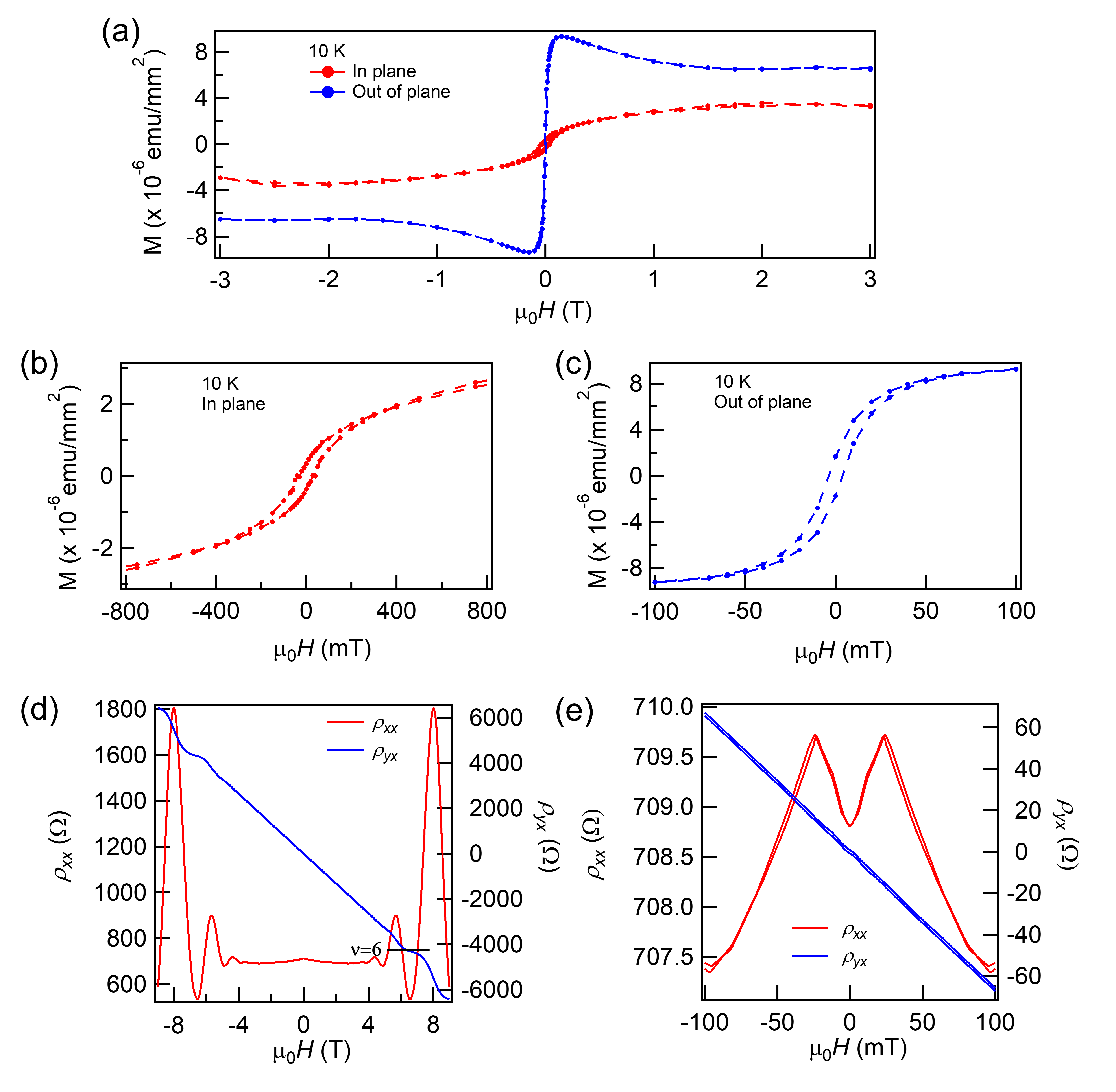
We first discuss SQUID magnetometry measurements of a 1 nm Mn-rich layer/ 7 nm Cd3As2 heterostructure that results from the delta-doping method with 6 repeats of (sub-monolayer MnAs/1.25 nm Cd3As2); the thicknesses in the final structure are estimated from HAADF-STEM measurements of a thicker sample using similar conditions with twice the thickness. The measurements were carried out in a Quantum Design SQUID magnetometer with the sample mounted in a straw for field parallel to and field normal to the sample plane. Figure 3 (a) shows the magnetization () versus field () at K for this sample with the field in plane and out-of-plane. A diamagnetic background has been subtracted in these plots. Zoomed in views of vs. for field in-plane (Fig. 3(b)) and out-of-plane (Fig. 3(c)) show hysteresis loops with a very large coercive field ( mT) in the former case and much smaller coercive field ( mT) in the latter. The behavior of the coercive field and the saturation field for the two field orientations are consistent with ferromagnetism in the sample with a strong out-of-plane magnetocrystalline anisotropy. This could arise from an inhomogenous distribution of Mn forming complex nanoscale cluster phases with the other elements present in the TEM analysis (primarily O, but also containing Cd and As). We note that the most commonly known compounds involving Mn and O (MnO and Mn3O4) are antiferromagnetic and feromagnetic, respectively. A more detailed understanding of the origin of ferromagnetism in such samples will require measurements such as x-ray magnetic circular dichroism and polarized neutron reflectometry.
Next, we discuss electrical transport in this 1 nm Mn-rich layer/ 7 nm Cd3As2 heterostructure. We fabricated the samples into 40 Hall bar devices using photolithography and Ar+ plasma dry etching. The top gate was defined by a 30 nm Al2O3 dielectric layer and Ti(5 nm)/Au(50 nm) contacts deposited by atomic layer deposition and electron beam evaporation, respectively. Magnetoresistance (MR) and Hall effect measurements were carried out in a Quantum Design Physical Properties Measurement System over a temperature range 2 K K and in magnetic fields up to T. All the MR and Hall effect data shown have been properly field symmetrized or anti-symmetrized, respectively. Figure 3(d) shows the results of such measurements at K. Surprisingly, despite the presence of the ferromagnetic overlayer in direct contact with the Cd3As2 film, we observe pronounced quantum oscillations and even an incipient quantum Hall effect indicated by a Hall resistance plateau corresponding to . We searched for possible signatures of an exchange coupling between the electrons in the Cd3As2 layer and Mn moments in the overlayer. Since the easy axis of the Mn-rich layer is out-of-plane according to our SQUID measurements, an exchange coupling between carriers in Cd3As2 and the Mn moments should lead to hysteresis in the field dependence of the Hall resistance and also to the MR from modifications to the quantum corrections to diffusive transport. Figure 3 (e) shows a careful sweep of the longitudinal MR and the Hall effect in the field range -0.1 T 0.1 T. The low field MR shows a non-monotonic dependence on magnetic field with an initial positive MR followed by a sudden change to a negative MR at a field close to the coercive field observed in SQUID magnetometry. The negative MR at fields higher than the saturation field of the ferromagnetic layer may indicate a reduction in spin-dependent scattering. In contrast, pristine Cd3As2 films grown under similar conditions only show a positive MR for field perpendicular to the sample plane (see Supplementary material at xxx). We do not see any obvious signs of hysteretic or non-linear Hall resistance. It is possible that with the step size used in the magneto-transport measurements (0.01 T), we might not be able to resolve these differences given how quickly the magnetization saturates with field along the anisotropy axis and the narrowness of hysteresis loop.
To further understand the effect of the Mn-rich overlayer on quantum transport, we analyzed the quantum oscillations in the heterostructure and compared the behavior with similar measurements in pure Cd3As2 thin films. For the 1 nm Mn-rich layer/ 7 nm Cd3As2 heterostructure, the amplitude of quantum oscillations gradually decreased with increasing temperature but remained finite up to about K as shown in Fig.4(a). We note that the quantum Hall plateau mentioned earlier was observable up to K in Fig. 4(b). To extract the carrier density, mobility, and effective mass of the carriers involved in quantum transport, we studied the temperature dependence of the quantum oscillations (Figs. 4(c) and 4(d)). The carrier density and mobility were calculated using both the Drude model and quantum oscillations. Using the Drude model, we find a carrier density and a mobility cm2/V/s at K. The analysis of quantum oscillations yields and cm2/V/s. The higher carrier density and lower carrier mobility deduced from Drude analysis compared to that obtained from quantum oscillations indicates the presence of low-mobility carriers that do not contribute to the quantum oscillations. The band origin of the low mobility carriers is not clear at this stage. By fitting the amplitude of the quantum oscillations using the standard Lifshitz-Kosevich formula [21], we extracted an effective mass . This light effective mass is due to the Dirac dispersion and is in good agreement with previous studies of Cd3As2 thin films [35, 24, 21].
Figure 4(c) also shows the carrier density and the mobility of a pure 7 nm Cd3As2 thin film (at K) calculated from the Drude model; this film was grown under nominally identical conditions (substrate temperature and Cd:As flux ratio) to those used for the growth of Mn-delta-doped samples. The carrier density in the pure film is about 20% higher and the Drude mobility is about 50% lower than in the Mn-doped film. Our findings suggest that the Mn-rich layer does not contribute to the transport signal and perhaps passivates the Cd3As2 layers underneath from electronegative OH-surface adsorbates [36].
Although the Mn-rich layer lies between the Cd3As2 layer and the top gate, it does not appear to affect the efficiency of the top gate. As shown in Fig. 4(e) and 4(f), the chemical potential of the heterostructure can be tuned from n-type to p-type by applying a top gate voltage. The quantum oscillations are only observed in the positive gate voltage regime, indicating the higher mobility of n-type carriers. We also note that the emerging quantum Hall plateaus are observable only around zero gate voltage, which is close to the Dirac point of the Cd3As2 layer. Away from the Dirac point, the quantum Hall plateaus disappear because of the high carrier density in the n-type regime and the low mobility in the p-type regime.
We now discuss our results in the context of prior studies of pristine (non-magnetic) Cd3As2 thin films, in particular those grown on (111) GaSb/GaAs. The integer quantum Hall effect was initially observed in a (112)-oriented Cd3As2 thin film of 20 nm thickness [24], followed by observations in similarly grown films whose thicknesses ranged from 10 nm - 60 nm [25]. While it is clear that the integer quantum Hall effect in these Cd3As2 films indicates quantum transport in a two-dimensional (2D) electron gas, a complete understanding of its origin is still lacking. A systematic study of the thickness-dependence of the quantum transport appears to rule out the role of Weyl orbits in the experimentally observed quantum Hall effect. [25] This hypothesis is consistent with our observation of an incipient integer quantum Hall effect in an even thinner (7 nm) Cd3As2 film than in these earlier studies; in addition, we observe the quantum Hall effect in the presence of a highly structurally disordered ferromagnetic interface at the top surface. We note that recent density functional theory calculations indicate that surface Fermi arcs likely survive in Cd3As2 films down to the thicknesses studied experimentally here. [37] However, these Fermi arc states on the top surface would presumably not survive in the presence of the disordered magnetic layer, especially with an out-of-plane magnetization. Our results appear to suggest that the wave function of the 2D electron system in ultrathin Cd3As2 films, likely built from Fermi arc states and quantum confined bulk states, has a maximum located away from the top and bottom surfaces, thus being immune to perturbation by the magnetism on the top surface. At this stage, however, we do not have a rigorous calculation to support this speculation.
III Summary
In summary, we have shown that conventional magnetic doping approaches to introducing ferromagnetism into Cd3As2 by MBE result in a phase separation with a Mn-rich near-surface layer capping a pristine Cd3As2 film since Mn likely acts as surfactant. The Mn-rich region shows out-of-plane magnetic anisotropy in SQUID measurements. Surprisingly, this ferromagnetic Mn-rich layer does not negatively affect the quantum transport in the Cd3As2 underneath. On the contrary, compared with pure Cd3As2 thin films grown under identical conditions, the presence of the Mn surfactant lowers the carrier density so that the chemical potential is close to the Dirac point and leads to an enhanced electron mobility. The resulting 1 nm Mn-rich layer/ 7 nm Cd3As2 films show an emergent quantum Hall effect in transport measurements. This should become more robust if the samples are measured at lower temperature and at higher magnetic fields. Measurements at dilution fridge temperatures may also reveal emergent physics resulting from the presence of the ferromagnetic overlayer. Although it is hard to dope Mn directly into Cd3As2 using MBE, it is worthwhile using other techniques such as polarized-neutron reflectometry to search for magnetic proximity effects of the easy-plane ferromagnetism on the Cd3As2 underneath. Our study indicates that extreme caution is called for in relying on magnetotransport data alone as a sign of broken time-reversal symmetry in magnetically-doped Cd3As2 films, especially in the absence of electron microscopy data [30].
Acknowledgements.
This project was supported by the Institute for Quantum Matter under DOE EFRC grant DE-SC0019331 (RX,NS). The magnetometry measurements were supported by a grant from the University of Chicago (JR,NS). The electron microscopy effort (JH,AM) was supported by SMART, one of seven centers of nCORE, a Semiconductor Research Corporation program, sponsored by the National Institute of Standards and Technology (NIST) and by the College of Science and Engineering Characterization Facility, University of Minnesota, which has received capital equipment funding from the National Science Foundation through the UMN MRSEC under Award Number DMR-2011401. We thank Chris Leighton, Paul Crowell, Yi Li, and Junyi Zhang for useful comments.References
- Macdonald et al. [2005] A. H. Macdonald, P. Schiffer, and N. Samarth, Ferromagnetic semiconductors: Moving beyond (Ga,Mn)As, Nat. Mater. 4, 195 (2005).
- Liu et al. [2008] C.-X. Liu, X.-L. Qi, X. Dai, Z. Fang, and S.-C. Zhang, Quantum anomalous Hall effect in Hg MnyTe quantum wells, Phys. Rev. Lett. 101, 146802 (2008).
- Yu et al. [2010] R. Yu, W. Zhang, H.-J. Zhang, S.-C. Zhang, X. Dai, and Z. Fang, Quantized anomalous Hall effect in magnetic topological insulators, Science 329, 61 (2010).
- Xu et al. [2012] S.-Y. Xu, M. Neupane, C. Liu, D. Zhang, A. Richardella, L. A. Wray, N. Alidoust, M. Leandersson, T. Balasubramanian, J. Sánchez-Barriga, O. Rader, G. Landolt, B. Slomski, J. H. Dil, J. Osterwalder, T.-R. Chang, H.-T. Jeng, H. Lin, A. Bansil, N. Samarth, and M. Z. Hasan, Hedgehog spin texture and Berry’s phase tuning in a magnetic topological insulator, Nat. Phys. 8, 616 (2012).
- Chang et al. [2013a] C.-Z. Chang, J. Zhang, M. Liu, Z. Zhang, X. Feng, K. Li, L.-L. Wang, X. Chen, X. Dai, Z. Fang, X.-L. Qi, S.-C. Zhang, Y. Wang, K. He, X.-C. Ma, and Q.-K. Xue, Thin films of magnetically doped topological insulator with carrier-independent long-range ferromagnetic order, Adv. Mater. 25, 1065 (2013a).
- Dietl and Ohno [2014] T. Dietl and H. Ohno, Dilute ferromagnetic semiconductors: physics and spintronic structures, Rev. Mod. Phys. 86, 187 (2014).
- Chang et al. [2013b] C.-Z. Chang, J. Zhang, X. Feng, J. Shen, Z. Zhang, M. Guo, K. Li, Y. Ou, P. Wei, L.-L. Wang, Z.-Q. Ji, Y. Feng, S. Ji, X. Chen, J. Jia, X. Dai, Z. Fang, S.-C. Zhang, K. He, Y. Wang, L. Lu, X.-C. Ma, and Q.-K. Xue, Experimental observation of the Quantum anomalous Hall effect in a magnetic topological insulator, Science 340, 167 (2013b).
- Kandala et al. [2015] A. Kandala, A. Richardella, S. Kempinger, C.-X. Liu, and N. Samarth, Giant anisotropic magnetoresistance in a quantum anomalous Hall insulator, Nat. Commun. 6, 1 (2015).
- Chang et al. [2015] C.-Z. Chang, W. Zhao, D. Y. Kim, H. Zhang, B. A. Assaf, D. Heiman, S.-C. Zhang, C.-x. Liu, M. H. W. Chan, and J. S. Moodera, High-precision realization of robust quantum anomalous Hall state in a hard ferromagnetic topological insulator, Nat. Mater. 14, 473 (2015).
- Liu et al. [2014a] Z. K. Liu, B. Zhou, Y. Zhang, Z. J. Wang, H. M. Weng, D. Prabhakaran, S.-K. Mo, Z. X. Shen, Z. Fang, X. Dai, Z. Hussain, and Y. L. Chen, Discovery of a three-dimensional topological Dirac semimetal, Na3Bi, Science 343, 864 (2014a).
- Xu et al. [2015] S.-Y. Xu, C. Liu, S. K. Kushwaha, R. Sankar, J. W. Krizan, I. Belopolski, M. Neupane, G. Bian, N. Alidoust, T.-R. Chang, H.-T. Jeng, C.-Y. Huang, W.-F. Tsai, H. Lin, P. P. Shibayev, F.-C. Chou, R. J. Cava, and M. Z. Hasan, Observation of Fermi arc surface states in a topological metal, Science 347, 294 (2015).
- Liu et al. [2014b] Z. K. Liu, J. Jiang, B. Zhou, Z. J. Wang, Y. Zhang, H. Weng, D. Prabhakaran, S. K. Mo, H. Peng, P. Dudin, T. Kim, M. Hoesch, Z. Fang, X. Dai, Z. X. Shen, D. L. Feng, H. Z., and Y. L. Chen, A stable three-dimensional topological Dirac semimetal Cd3As2, Nat. Mater. 13, 677 (2014b).
- Neupane et al. [2014] M. Neupane, S.-Y. Xu, R. Sankar, N. Alidoust, G. Bian, C. Liu, I. Belopolski, T.-R. Chang, H.-T. Jeng, H. Lin, A. Bansil, F. Chou, and M. Z. Hasan, Observation of a three-dimensional topological Dirac semimetal phase in high-mobility Cd3As2, Nat. Commun. 5, 1 (2014).
- Yi et al. [2014] H. Yi, Z. Wang, C. Chen, Y. Shi, Y. Feng, A. Liang, Z. Xie, S. He, J. He, Y. Peng, X. Liu, Y. Liu, L. Zhao, G. Liu, X. Dong, J. Zhang, M. Nakatake, M. Arita, K. Shimada, H. Namatame, M. Taniguchi, Z. Xu, C. Chen, X. Dai, Z. Fang, and X. J. Zhou, Evidence of topological surface state in three-dimensional Dirac semimetal Cd3As2, Sci. Rep. 4, 1 (2014).
- Armitage et al. [2018] N. P. Armitage, E. J. Mele, and A. Vishwanath, Weyl and Dirac semimetals in three-dimensional solids, Rev. Mod. Phys. 90, 015001 (2018).
- Weyl [1929] H. Weyl, Elektron und gravitation. i, Z. Phys. 56, 330 (1929).
- Burkov and Balents [2011] A. A. Burkov and L. Balents, Weyl semimetal in a topological insulator multilayer, Phys. Rev. Lett. 107, 127205 (2011).
- Wang et al. [2013] Z. Wang, H. Weng, Q. Wu, X. Dai, and Z. Fang, Three-dimensional Dirac semimetal and quantum transport in Cd3As2, Phys. Rev. B 88, 125427 (2013).
- Baidya and Vanderbilt [2020] S. Baidya and D. Vanderbilt, First-principles theory of the dirac semimetal Cd3As2 under Zeeman magnetic field, Phys. Rev. B 102, 165115 (2020).
- Schumann et al. [2016] T. Schumann, M. Goyal, H. Kim, and S. Stemmer, Molecular beam epitaxy of Cd3As2 on a III-V substrate, APL Mater. 4, 126110 (2016).
- Uchida et al. [2017] M. Uchida, Y. Nakazawa, S. Nishihaya, K. Akiba, M. Kriener, Y. Kozuka, A. Miyake, Y. Taguchi, M. Tokunaga, N. Nagaosa, Y. Tokura, and M. Kawasaki, Quantum Hall states observed in thin films of Dirac semimetal Cd3As2, Nat. Commun. 8, 1 (2017).
- Liu et al. [2015] Y. Liu, C. Zhang, X. Yuan, T. Lei, C. Wang, D. Di Sante, A. Narayan, L. He, S. Picozzi, S. Sanvito, R. Che, and F. Xiu, Gate-tunable quantum oscillations in ambipolar Cd3As2 thin films, NPG Asia Mater. 7, e221 (2015).
- Yanez et al. [2021] W. Yanez, Y. Ou, R. Xiao, J. Koo, J. T. Held, S. Ghosh, J. Rable, T. Pillsbury, E. G. Delgado, K. Yang, J. Chamorro, A. J. Grutter, P. Quarterman, A. Richardella, A. Sengupta, T. McQueen, J. A. Borchers, K. A. Mkhoyan, B. Yan, and N. Samarth, Spin and charge interconversion in dirac-semimetal thin films, Phys. Rev. Applied 16, 054031 (2021).
- Schumann et al. [2018] T. Schumann, L. Galletti, D. A. Kealhofer, H. Kim, M. Goyal, and S. Stemmer, Observation of the quantum Hall effect in confined films of the three-dimensional Dirac semimetal cd3as2, Phys. Rev. Lett. 120, 016801 (2018).
- Galletti et al. [2019] L. Galletti, T. Schumann, D. A. Kealhofer, M. Goyal, and S. Stemmer, Absence of signatures of Weyl orbits in the thickness dependence of quantum transport in cadmium arsenide, Phys. Rev. B 99, 201401(R) (2019).
- Liu et al. [2019] D. F. Liu, A. J. Liang, E. K. Liu, Q. N. Xu, Y. W. Li, C. Chen, D. Pei, W. J. Shi, S. K. Mo, P. Dudin, T. Kim, C. Cacho, G. Li, Y. Sun, L. X. Yang, Z. K. Liu, S. S. P. Parkin, C. Felser, and Y. L. Chen, Magnetic Weyl semimetal phase in a Kagomé crystal, Science 365, 1282 (2019).
- Morali et al. [2019] N. Morali, R. Batabyal, P. K. Nag, E. Liu, Q. Xu, Y. Sun, B. Yan, C. Felser, N. Avraham, and H. Beidenkopf, Fermi-arc diversity on surface terminations of the magnetic Weyl semimetal Co3Sn2S2, Science 365, 1286 (2019).
- Belopolski et al. [2019] I. Belopolski, K. Manna, D. S. Sanchez, G. Chang, B. Ernst, J. Yin, S. S. Zhang, T. Cochran, N. Shumiya, H. Zheng, B. Singh, G. Bian, D. Multer, M. Litskevich, X. Zhou, S.-M. Huang, B. Wang, T.-R. Chang, S.-Y. Xu, A. Bansil, C. Felser, H. Lin, and M. Z. Hasan, Discovery of topological Weyl fermion lines and drumhead surface states in a room temperature magnet, Science 365, 1278 (2019).
- Li and Haldane [2018] Y. Li and F. D. M. Haldane, Topological nodal Cooper pairing in doped Weyl metals, Phys. Rev. Lett. 120, 067003 (2018).
- Liu et al. [2018] Y. Liu, R. Tiwari, A. Narayan, Z. Jin, X. Yuan, C. Zhang, F. Chen, L. Li, Z. Xia, S. Sanvito, P. Zhou, and F. Xiu, Cr doping induced negative transverse magnetoresistance in Cd3As2 thin films, Phys. Rev. B 97, 085303 (2018).
- Wang et al. [2020] H. Wang, J. Ma, Q. Wei, and J. Zhao, Mn doping effects on the gate-tunable transport properties of Cd3As2 films epitaxied on GaAs, Journal of Semiconductors 41, 072903 (2020).
- Crooker et al. [1995] S. A. Crooker, D. A. Tulchinsky, J. Levy, D. D. Awschalom, R. Garcia, and N. Samarth, Enhanced spin interactions in digital magnetic heterostructures, Phys. Rev. Lett. 75, 505 (1995).
- Kawakami et al. [2000] R. K. Kawakami, E. Johnston-Halperin, L. F. Chen, M. Hanson, N. Guébels, J. S. Speck, A. C. Gossard, and D. D. Awschalom, (Ga,Mn)As as a digital ferromagnetic heterostructure, Appl. Phys. Lett. 77, 2379 (2000).
- Ril et al. [2017] A. I. Ril, I. V. Fedorchenko, S. F. Marenkin, A. V. Kochura, and A. E. Kuz’ko, Phase equilibria in the CdAs2–Cd3As2–MnAs ternary system, Russ. J. Inorg. Chem. 62, 976 (2017).
- Zhao et al. [2015] Y. Zhao, H. Liu, C. Zhang, H. Wang, J. Wang, Z. Lin, Y. Xing, H. Lu, J. Liu, Y. Wang, S. M. Brombosz, Z. Xiao, S. Jia, X. C. Xie, and J. Wang, Anisotropic Fermi surface and quantum limit transport in high mobility three-dimensional Dirac semimetal Cd3As2, Phys. Rev. X 5, 031037 (2015).
- Galletti et al. [2018] L. Galletti, T. Schumann, T. E. Mates, and S. Stemmer, Nitrogen surface passivation of the Dirac semimetal Cd3As2, Phys. Rev. Mater. 2, 124202 (2018).
- Villar Arribi et al. [2020] P. Villar Arribi, J.-X. Zhu, T. Schumann, S. Stemmer, A. A. Burkov, and O. Heinonen, Topological surface states in strained Dirac semimetal thin films, Phys. Rev. B 102, 155141 (2020).
- Wang et al. [2012] Z. Wang, Y. Sun, X.-Q. Chen, C. Franchini, G. Xu, H. Weng, X. Dai, and Z. Fang, Dirac semimetal and topological phase transitions in A3Bi (A= Na, K, Rb), Phys. Rev. B 85, 195320 (2012).
- Young et al. [2012] S. M. Young, S. Zaheer, J. C. Teo, C. L. Kane, E. J. Mele, and A. M. Rappe, Dirac semimetal in three dimensions, Phys. Rev. Lett. 108, 140405 (2012).