Single-shot readout in graphene quantum dots
Abstract
Electrostatically defined quantum dots in bilayer graphene offer a promising platform for spin qubits with presumably long coherence times due to low spin–orbit coupling and low nuclear spin density. We demonstrate two different experimental approaches to measure the decay times of excited states. The first is based on direct current measurements through the quantum device. Pulse sequences are applied to control the occupation of ground and excited states. We observe a lower bound for the excited state decay on the order of hundred microseconds. The second approach employs a capacitively coupled charge sensor to study the time dynamics of the excited state using the Elzerman technique. We find that the relaxation time of the excited state is of the order of milliseconds. We perform single-shot readout of our two-level system with a visibility of , which is an important step for developing a quantum information processor in graphene.
I Introduction
Spin qubits in semiconductors [1, 2] have the advantage that the operation and fabrication of gate electrodes are similar to classical transistors. High-quality qubits have been demonstrated on traditional bulk MOSFETs [3, 4, 5] as well as on \Romannum3-\Romannum5 [6, 7, 8], silicon- [9, 10, 11, 12] and germanium- [13] based heterostructures. Furthermore, semi-industrial structures compatible with industrial Si-technologies, such as fully-depleted silicon-on-insulator (FD-SOI) transistors [14] and fin field-effect transistors (FinFETs) [15], have been investigated.
Graphene offers several advantages as a host material for spin qubits, namely naturally low nuclear spin concentrations and weak spin–orbit interactions, similar to Si. In addition, the 2D nature of graphene allows for much smaller and possibly more strongly coupled quantum devices [16]. Furthermore, bilayer graphene quantum dots (QDs) offer the flexibility of bipolar operation [17]. Compared to the mature Si-based technology, the development of quantum devices in graphene is in its infancy. Recent advances in the controllability of individual states in single QDs [17, 18, 19, 20] and double QDs [21, 22], as well as the implementation of charge detection [23], enable the realization of spin qubits based on electrostatically defined QDs in bilayer graphene. Major milestones such as qubit manipulation and detection have yet to be achieved to unlock the qubit potential of graphene.
Single-shot readout is an essential first step towards building a universal quantum computer and implementing quantum algorithms and quantum error detection. In order to reach the single-shot readout limit, it is critical for the excited state relaxation time to be longer than the measurement time to resolve a single charging event. We first investigate the relaxation time by measuring the current flowing through a QD [24, 25], which allows us to extract a lower bound only, similar to previous experiments [26]. In order to study the time dynamics of the excited state beyond the microsecond regime, we add a charge detector to the device design and perform time-resolved measurements of the tunneling events in the QD. This allows us to perform single-shot readout of the two-level system using the Elzerman technique [27]. We estimate the relaxation time to be in the millisecond regime which is a few orders of magnitude longer than typical spin-qubit operation times[28, 29].
II Pulsed-gate spectroscopy
A false-color atomic force micrograph of the device is shown in Fig. 1(a). It consists of a hBN encapsulated bilayer graphene flake on top of a global graphite back gate with gold electrodes patterned on top. The gate layers are separated by atomic-layer-deposited aluminium oxide [17]. We form an -type channel connecting source and drain by operating the back gate at and the split gates at . Three finger gates are used to control the potential locally along the channel [see Fig. 1(a)]. The outer two finger gates TL and TR act as tunable tunnel barriers separating the QD from the left and right reservoirs. With increasingly negative voltage applied to the middle finger gate (the plunger gate), we locally lower the Fermi energy set by the back gate, subsequently loading holes into the QD forming below the gate. The sample is mounted in a dilution refrigerator with a base-temperature of on a printed circuit board equipped with low-pass-filtered DC lines and impedance-matched AC lines to perform pulsed-gate experiments. The plunger gate is connected to a bias-tee allowing for DC and AC control [e.g., applying a pulse as sketched in Fig. 1(b)] while all other gates and the ohmic contacts are connected to DC lines only.
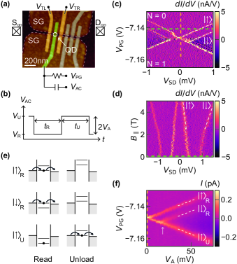
We first define our two-level system. Due to spin and valley degrees of freedom in bilayer graphene, the single-particle orbital states are four-fold degenerate [18, 30]. A perpendicular magnetic field, , lifts the degeneracy due to the spin (s) and valley (v) Zeeman effect following , with the spin -factor , the valley -factor and the Bohr magneton . Typical values around [17] ensure that at electron temperatures below , the two lowest energy levels are valley polarized already at perpendicular magnetic fields . As we operate our device at much higher fields, above , we can consider our QD as an effective two-level spin system with the ground state (GS) and the excited state (ES) energetically split by with the zero-field spin orbit splitting with typical values on the order of [20, 31, 32, 22].
To experimentally access the single-particle spectrum we perform finite-bias spectroscopy measurements around the to hole transition at [Fig. 1(c)]. The two lowest -polarized energy states and , from now on denoted as and for ease of notation, are well observable while the -states are split off and would only become visible for a larger bias window.
To confirm the nature of the excited state we apply an additional in-plane magnetic field , which only couples to the spin degree of freedom. Keeping the perpendicular magnetic field and the plunger gate voltage fixed [horizontal dashed line in Fig. 1(c)] we perform finite-bias spectroscopy measurements, varying the in-plane magnetic field [Fig. 1(d)]. The splitting as a function of magnetic field corresponds to a -factor of 2 and a zero-field spin–orbit splitting , consistent with a spin excited state.
We then perform transient current spectroscopy measurements at a source–drain voltage to study the relaxation of the excited state to the ground state. We apply an AC pulse additional to the DC voltage on the plunger gate, effectively shifting the QD states with respect to the Fermi level of the reservoirs in time. We start with two-level pulses each consisting of a read and an unload phase as shown in Fig. 1(b) with corresponding voltages and and pulse widths and . During , both and are pulsed above the Fermi level of the leads and the QD is emptied. During , if is aligned with we observe a steady current. If is aligned with during while lies below, holes can only tunnel through the QD excited state until one of them relaxes with a spin-flip or until direct tunneling from the leads into the ground state occurs. This effectively blocks transport until the QD gets emptied again in the subsequent unload phase. Fig. 1(f) shows the current through the QD as a function of pulse amplitude and for . We observe the splitting of the Coulomb resonance into two peaks, corresponding to transient current through the ground state of the read level, , and the unload level, . At , the peaks are separated by . This splitting is consistent with the total attenuation of the high-frequency line of our setup. The slope of the ground state splitting, together with the plunger gate lever arm, give us the conversion factor from pulse amplitude to energy scale , where and . For pulse amplitudes larger than the Zeeman splitting [indicated in Fig. 1(f)] the current peak corresponding to a transient current through the excited state of the read level, , becomes visible as well. We observe the peak, because a sufficiently high perpendicular magnetic field is applied. This not only lifts spin and valley degeneracies but also reduces the tunneling rates between the QD and the reservoirs. At low perpendicular magnetic field is not visible, as the reduction of tunneling rates solely by voltages applied to the tunnel barrier gates TL and TR is not sufficient in this device (see Ref. [23]).
The longer the QD stays in the read phase, the more likely the hole relaxes into the ground state . Therefore, studying the dependence of the amplitude of on the pulse width allows us to extract information about the relaxation time. However, two-level pulsed-gate spectroscopy only allows one to extract a lower bound for , as this measurement scheme cannot distinguish between relaxation and direct tunneling into the ground state during the read-phase. Already Ref. [33] suffered from this limitation, stating a lower bound of . To improve on this limitation, we extend the pulsing sequence to four-level pulses with added load and wait phases in which both and are pulsed below the bias window [34, 26]. The voltage and time for the load phase is chosen such that the time-integral over voltages in one pulse sequence is zero, in order to avoid charging up the bias-tee. The corresponding four-level pulse scheme is depicted in Fig. 2(a) with pulse widths and and voltages , , and for the respective pulse periods. During the load and the wait phases both and levels are below the bias window, allowing a hole to tunnel into either one of the two states. During , the excited state is aligned with the Fermi level of the leads while the ground state is still below, allowing for spin-selective tunneling.
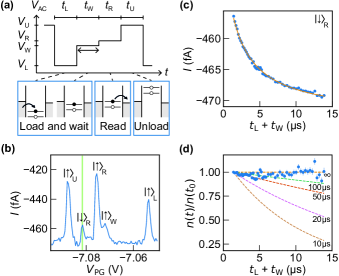
Applying the four-level pulsing scheme while sweeping the DC plunger gate voltage results in a current trace as shown in Fig. 2(b). Assigning the observed current peaks to ground state and excited state levels being aligned with the bias window during various pulse phases, we identify the peak (shaded in green), originating from holes tunneling through the excited state from source to drain during the read phase. If it relaxes to before the readout, it does not contribute to this current as it cannot tunnel out of the QD, making the amplitude of the current peak a measure of the relaxation. Therefore, we investigate the amplitude of the current peak, , as a function of the waiting time as shown in Fig. 2(c). We find that the current can be fitted to [34] in the limit , and therefore effectively to with high confidence. In these expressions, is the average number of charge carriers per pulse cycle, is the total duration of the four-level pulse, and is the background current level. This implies that, within our measurement time window the decay of the measured current through is dominated by the signal strength reducing as the pulse cycle time becomes longer for increasing . Multiplying with the total time we stay below , , we find the normalized probability of the hole still being in the excited state after the load and wait phase as a function of loading and waiting time, , shown in Fig. 2(d). Based on this we conservatively estimate a lower bound for the relaxation time . The data was acquired over 8 hours over which the background current fluctuation can be larger than and lead to an uncertainty in the offset current. Careful determination of is crucial as it affects the slope in Fig. 2(d). Further extending the waiting time inevitably leads to vanishingly small current beyond the detection limit of transport measurements. To overcome the signal strength limit, a more advanced readout mechanism is required.
III Single-shot excited state detection
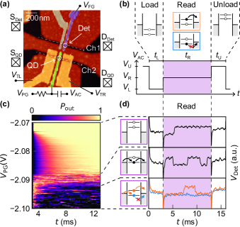
Recent progress in fabrication techniques enabled the realization of a fully electrostatically defined device with an integrated charge detector as described in Ref. [23]. The device shown in Fig. 3(a) consists of two channels separated by a depletion region underneath a wide middle gate. The QD is formed beneath the plunger gate in channel 2 whereas TL and TR serve as tunnel barriers to the leads as in the previous sample. The charge detector is based on a second QD formed below a single finger gate (FG) in the current biased channel 1. A charge carrier tunneling on or off the QD in channel 2 changes the electrostatic potential in its surroundings, therefore also in the nearby sensing QD in channel 1. This potential change shifts the Coulomb resonances in the sensing QD and leads to a step-like change in the voltage across channel 1, if the sensing QD is tuned to the steep slope of a conductance resonance.
At a perpendicular magnetic field of , we find an excited state split from the ground state by about . We exclude an orbital excitation, as the expected orbital splitting is a few . With an out-of-plane magnetic field of , typical valley splittings are - , with a valley -factor of 10 - 100 [17]. Therefore, the excited state is probably a spin state with and a spin-orbit coupling [35].
For the single-shot charge detection experiment, we follow the scheme introduced by Elzerman in Ref. [27]. Fig. 3(b) shows the voltage pulses applied to the plunger gate PG. Again, in the load phase either the GS or the ES can be loaded as both energy levels reside below the Fermi energy of the leads. During the loading time the charge carrier is trapped on the QD and Coulomb blockade prevents an additional hole from entering. After the pulse amplitude is changed to such that the energy level of the ES is pushed above while the GS level remains below. Therefore, the charge carrier can only tunnel off the QD if it was loaded onto the ES in the previous phase. Once the charge carrier has left the QD from the excited state, the Coulomb blockade is lifted and another charge carrier can tunnel into the GS. The combination of these two processes, tunneling out from the excited state, followed by tunneling into the ground state, leads to a characteristic ‘blip’ in the detector voltage, indicative of excited state loading during the load phase. Note that here we pulse the ES above of the leads, in contrast to the transport measurements before, where we aligned the ES level with the leads during the read phase. After we enter the unload phase, where the pulse amplitude is changed to , and both energy levels are pushed above emptying the QD. As a response to the three-level pulse we expect a change of voltage across the sensing QD consisting of two contributions. First, due to capacitive coupling between PG and the sensing QD the voltage will change proportionally to the applied pulse amplitude. Second, the voltage across the sensing QD traces the charge occupation of the QD, stepping up or down as soon as a charge carrier tunnels on or off the QD. Whenever we load the GS during load phase, the voltage trace should stay flat during . Therefore, measuring whether the voltage trace shows a blip or not during the read out phase forms the basis of our single-shot readout mechanism.
To find the appropriate alignment of the read-level for ES-dependent tunneling we sweep while keeping the three-level pulse amplitude constant. We choose pulse widths and , long enough to allow the charge carrier to tunnel in and out of the QD. The pulse voltages and ensure that both energy levels are pushed below (above) of the leads during the load (unload) phase. Starting with being too high, both GS and ES levels lie above , such that the charge carrier can always tunnel off the QD regardless of being in the ES or the GS. The characteristic voltage trace in this regime only shows a step up corresponding to the unloading event, and then remains at this higher level as shown in Fig. 3(d) top panel. When lowering we enter the regime of random telegraph signal corresponding to the GS being aligned with of the leads such that a charge carrier can tunnel on and off the QD multiple times within the read phase as observed in Fig. 3(d) middle panel. Further decreasing we find the correct read level where we can distinguish between the GS and ES of the QD being occupied. A single blip at the beginning of the read phase corresponds to the ES tunneling off the QD and subsequent tunneling into the GS from the leads. A flat trace during indicates that the charge carrier was loaded into the GS during the load phase, and is thus trapped on the QD. Alternatively, the excited state could have been loaded, but it relaxed into the ground state, before it could tunnel out. In this region the condition is fulfilled and we can perform a single-shot projective measurement of the state of the charge carrier. Exemplary traces for the two cases are shown in Fig. 3(d) bottom panel, with the blue trace corresponding to the GS and the orange one with the characteristic ’blip’ corresponding to the ES.
Averaging the read-phase voltage across the sensing QD over 300 single-shot traces at different plunger gate voltages we estimate the probability of the QD being empty as a function of time for each cycle as shown in Fig. 3(c). The correct readout configuration shows a higher current in the beginning of the read phase, as observed in the lower part of Fig. 3(c). The excited state tunneling events can only be observed if the excited state does not decay into the ground state during the time it stays in the load phase . Thus, observing a ’blip’ makes us conclude that the relaxation time is on the order of milliseconds.
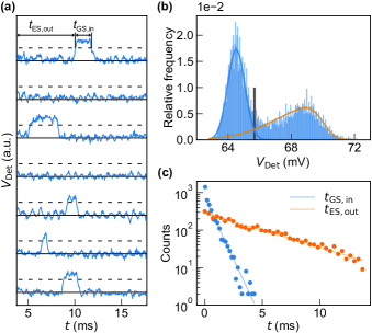
Typical experimental traces of the detector response in the read phase are shown in Fig. 4(a). If the trace surpasses the threshold voltage (dashed line) within the read phase window, it indicates that the hole occupied the ES during the previous load phase. Analyzing a data set consisting of 10’000 single-shots we extract the histogram of the peak values of shown in Fig 4(b). We identify two well-defined peaks indicating that the detector voltage has two favorable values corresponding to an additional hole being in the QD or not. By further analyzing the traces with a ’blip’, we extract the tunnel-out time of the ES and the tunnel-in time of the GS with fits to the data shown in Fig 4(c).
By choosing a threshold that optimizes the readout visibility [36, 37, 27], we obtain the ground state readout fidelity , the excited state readout fidelity , and the visibility . The readout fidelity is limited by finite measurement bandwidth and charge sensitivity. An improved device geometry could include a wider detector channel for higher detector conductance and an optimized ratio between channel separation and hBN thickness for stronger capacitive coupling between the charge sensor and the QD. Faster charge detection can be achieved by using a rf-charge detector [38, 39, 40], dispersive charge sensing by coupling the QDs to lumped-element LC tank circuit [41, 42, 43, 44], or by an on-chip superconducting resonator [45, 46, 47].
IV Conclusion
In conclusion, we first characterized the lifetime of excited states in a graphene QD through direct transport measurements. The measurement is limited by signal strength rather than the relaxation time, comparable to previous measurements performed in bilayer graphene QDs. In a second step we presented a QD device integrated with a capacitively coupled charge sensor capable of resolving a single charge tunneling event in the time-domain. The sensitivity of the charge detector enables excited state readout in the single-shot limit - an essential step towards a fully controllable quantum processor in graphene. Our result further indicates that the relaxation time is of the order of milliseconds, comparable to most semiconductor qubits encoded by electron spin, showing that spin qubits in bilayer graphene QDs are a promising platform.
V Acknowledgement
We are grateful for the technical support from Peter Märki, Thomas Bähler and the staff of the ETH FIRST cleanroom facility. We thank Luca Banszerus and Christian Volk for discussions. We acknowledge financial support by the European Graphene Flagship, the ERC Synergy Grant Quantropy, the European Union’s Horizon 2020 research and innovation programme under grant agreement number 862660/QUANTUM E LEAPS and NCCR QSIT (Swiss National Science Foundation) and under the Marie SKlodowska-Curie Grant Agreement Number 766025. KW and TT acknowledge support from the Element Strategy Initiative conducted by the MEXT, Japan, Grant Number JPMXP0112101001, JSPS KAKENHI Grant Number JP20H00354 and the CREST(JPMJCR15F3), JST.
References
- Loss and DiVincenzo [1998] D. Loss and D. P. DiVincenzo, Quantum computation with quantum dots, Phys. Rev. A 57, 120 (1998).
- Stano and Loss [2021] P. Stano and D. Loss, Review of performance metrics of spin qubits in gated semiconducting nanostructures (2021), arXiv:2107.06485 [cond-mat.mes-hall] .
- Veldhorst et al. [2014] M. Veldhorst, J. C. C. Hwang, C. H. Yang, A. W. Leenstra, B. de Ronde, J. P. Dehollain, J. T. Muhonen, F. E. Hudson, K. M. Itoh, A. Morello, and A. S. Dzurak, An addressable quantum dot qubit with fault-tolerant control-fidelity, Nature Nanotechnology 9, 981 (2014).
- Yang et al. [2019] C. H. Yang, K. W. Chan, R. Harper, W. Huang, T. Evans, J. C. C. Hwang, B. Hensen, A. Laucht, T. Tanttu, F. E. Hudson, S. T. Flammia, K. M. Itoh, A. Morello, S. D. Bartlett, and A. S. Dzurak, Silicon qubit fidelities approaching incoherent noise limits via pulse engineering, Nature Electronics 2, 151 (2019).
- Veldhorst et al. [2015] M. Veldhorst, C. H. Yang, J. C. C. Hwang, W. Huang, J. P. Dehollain, J. T. Muhonen, S. Simmons, A. Laucht, F. E. Hudson, K. M. Itoh, A. Morello, and A. S. Dzurak, A two-qubit logic gate in silicon, Nature 526, 410 (2015).
- Nakajima et al. [2020] T. Nakajima, A. Noiri, K. Kawasaki, J. Yoneda, P. Stano, S. Amaha, T. Otsuka, K. Takeda, M. R. Delbecq, G. Allison, A. Ludwig, A. D. Wieck, D. Loss, and S. Tarucha, Coherence of a driven electron spin qubit actively decoupled from quasistatic noise, Phys. Rev. X 10, 011060 (2020).
- Cerfontaine et al. [2014] P. Cerfontaine, T. Botzem, D. P. DiVincenzo, and H. Bluhm, High-fidelity single-qubit gates for two-electron spin qubits in gaas, Phys. Rev. Lett. 113, 150501 (2014).
- Nichol et al. [2017] J. M. Nichol, L. A. Orona, S. P. Harvey, S. Fallahi, G. C. Gardner, M. J. Manfra, and A. Yacoby, High-fidelity entangling gate for double-quantum-dot spin qubits, npj Quantum Information 3, 3 (2017).
- Xue et al. [2021] X. Xue, M. Russ, N. Samkharadze, B. Undseth, A. Sammak, G. Scappucci, and L. M. K. Vandersypen, Computing with spin qubits at the surface code error threshold (2021), arXiv:2107.00628 [quant-ph] .
- Zajac et al. [2018] D. M. Zajac, A. J. Sigillito, M. Russ, F. Borjans, J. M. Taylor, G. Burkard, and J. R. Petta, Resonantly driven cnot gate for electron spins, Science 359, 439 (2018).
- Yoneda et al. [2018] J. Yoneda, K. Takeda, T. Otsuka, T. Nakajima, M. R. Delbecq, G. Allison, T. Honda, T. Kodera, S. Oda, Y. Hoshi, et al., A quantum-dot spin qubit with coherence limited by charge noise and fidelity higher than 99.9%, Nature Nanotechnology 13, 102 (2018).
- Mills et al. [2021] A. R. Mills, C. R. Guinn, M. J. Gullans, A. J. Sigillito, M. M. Feldman, E. Nielsen, and J. R. Petta, Two-qubit silicon quantum processor with operation fidelity exceeding 99% (2021), arXiv:2111.11937 [quant-ph] .
- Hendrickx et al. [2021] N. W. Hendrickx, W. I. L. Lawrie, M. Russ, F. van Riggelen, S. L. de Snoo, R. N. Schouten, A. Sammak, G. Scappucci, and M. Veldhorst, A four-qubit germanium quantum processor, Nature 591, 580 (2021).
- Maurand et al. [2016] R. Maurand, X. Jehl, D. Kotekar-Patil, A. Corna, H. Bohuslavskyi, R. Laviéville, L. Hutin, S. Barraud, M. Vinet, M. Sanquer, et al., A cmos silicon spin qubit, Nature Communications 7, 13575 (2016).
- Camenzind et al. [2021] L. C. Camenzind, S. Geyer, A. Fuhrer, R. J. Warburton, D. M. Zumbühl, and A. V. Kuhlmann, A spin qubit in a fin field-effect transistor (2021), arXiv:2103.07369 [cond-mat.mes-hall] .
- Liu et al. [2021] Y. Liu, X. Duan, H.-J. Shin, S. Park, Y. Huang, and X. Duan, Promises and prospects of two-dimensional transistors, Nature 591, 43 (2021).
- Tong et al. [2021a] C. Tong, R. Garreis, A. Knothe, M. Eich, A. Sacchi, K. Watanabe, T. Taniguchi, V. Fal’ko, T. Ihn, K. Ensslin, and A. Kurzmann, Tunable valley splitting and bipolar operation in graphene quantum dots, Nano Letters 21, 1068 (2021a).
- Garreis et al. [2021] R. Garreis, A. Knothe, C. Tong, M. Eich, C. Gold, K. Watanabe, T. Taniguchi, V. Fal’ko, T. Ihn, K. Ensslin, and A. Kurzmann, Shell filling and trigonal warping in graphene quantum dots, Phys. Rev. Lett. 126, 147703 (2021).
- Möller et al. [2021] S. Möller, L. Banszerus, A. Knothe, C. Steiner, E. Icking, S. Trellenkamp, F. Lentz, K. Watanabe, T. Taniguchi, L. Glazman, V. Fal’ko, C. Volk, and C. Stampfer, Probing two-electron multiplets in bilayer graphene quantum dots (2021), arXiv:2106.08405 [cond-mat.mes-hall] .
- Kurzmann et al. [2021] A. Kurzmann, Y. Kleeorin, C. Tong, R. Garreis, A. Knothe, M. Eich, C. Mittag, C. Gold, F. K. de Vries, K. Watanabe, T. Taniguchi, V. Fal’ko, Y. Meir, T. Ihn, and K. Ensslin, Kondo effect and spin–orbit coupling in graphene quantum dots, Nature Communications 12, 6004 (2021).
- Tong et al. [2021b] C. Tong, A. Kurzmann, R. Garreis, W. W. Huang, S. Jele, M. Eich, L. Ginzburg, C. Mittag, K. Watanabe, T. Taniguchi, K. Ensslin, and T. Ihn, Pauli blockade of tunable two-electron spin and valley states in graphene quantum dots (2021b), arXiv:2106.04722 [cond-mat.mes-hall] .
- Banszerus et al. [2021a] L. Banszerus, S. Möller, C. Steiner, E. Icking, S. Trellenkamp, F. Lentz, K. Watanabe, T. Taniguchi, C. Volk, and C. Stampfer, Spin-valley coupling in single-electron bilayer graphene quantum dots, Nature Communications 12, 5250 (2021a).
- Kurzmann et al. [2019] A. Kurzmann, H. Overweg, M. Eich, A. Pally, P. Rickhaus, R. Pisoni, Y. Lee, K. Watanabe, T. Taniguchi, T. Ihn, and K. Ensslin, Charge detection in gate-defined bilayer graphene quantum dots, Nano Letters 19, 5216 (2019).
- Fujisawa et al. [2001] T. Fujisawa, Y. Tokura, and Y. Hirayama, Transient current spectroscopy of a quantum dot in the coulomb blockade regime, Phys. Rev. B 63, 081304 (2001).
- Hanson et al. [2003] R. Hanson, B. Witkamp, L. M. K. Vandersypen, L. H. W. van Beveren, J. M. Elzerman, and L. P. Kouwenhoven, Zeeman energy and spin relaxation in a one-electron quantum dot, Phys. Rev. Lett. 91, 196802 (2003).
- Banszerus et al. [2021b] L. Banszerus, K. Hecker, S. Möller, E. Icking, K. Watanabe, T. Taniguchi, C. Volk, and C. Stampfer, Spin relaxation in a single-electron graphene quantum dot (2021b), arXiv:2110.13051 [cond-mat.mes-hall] .
- Elzerman et al. [2004] J. M. Elzerman, R. Hanson, L. H. Willems van Beveren, B. Witkamp, L. M. K. Vandersypen, and L. P. Kouwenhoven, Single-shot read-out of an individual electron spin in a quantum dot, Nature 430, 431 (2004).
- Koppens et al. [2006] F. H. L. Koppens, C. Buizert, K. J. Tielrooij, I. T. Vink, K. C. Nowack, T. Meunier, L. P. Kouwenhoven, and L. M. K. Vandersypen, Driven coherent oscillations of a single electron spin in a quantum dot, Nature 442, 766 (2006).
- Hendrickx et al. [2020] N. W. Hendrickx, W. I. L. Lawrie, L. Petit, A. Sammak, G. Scappucci, and M. Veldhorst, A single-hole spin qubit, Nature Communications 11, 3478 (2020).
- Knothe and Fal’ko [2020] A. Knothe and V. Fal’ko, Quartet states in two-electron quantum dots in bilayer graphene, Phys. Rev. B 101, 235423 (2020).
- Konschuh et al. [2012] S. Konschuh, M. Gmitra, D. Kochan, and J. Fabian, Theory of spin-orbit coupling in bilayer graphene, Phys. Rev. B 85, 115423 (2012).
- Huertas-Hernando et al. [2006] D. Huertas-Hernando, F. Guinea, and A. Brataas, Spin-orbit coupling in curved graphene, fullerenes, nanotubes, and nanotube caps, Phys. Rev. B 74, 155426 (2006).
- Banszerus et al. [2021c] L. Banszerus, K. Hecker, E. Icking, S. Trellenkamp, F. Lentz, D. Neumaier, K. Watanabe, T. Taniguchi, C. Volk, and C. Stampfer, Pulsed-gate spectroscopy of single-electron spin states in bilayer graphene quantum dots, Phys. Rev. B 103, L081404 (2021c).
- Fujisawa et al. [2002] T. Fujisawa, D. G. Austing, Y. Tokura, Y. Hirayama, and S. Tarucha, Allowed and forbidden transitions in artificial hydrogen and helium atoms, Nature 419, 278 (2002).
- [35] For a detailed analysis of the nature of the excited state, magnetic field-dependent finite-bias measurements are required. They are challenging, however, due to the low tunneling rate through the QD and its non-monotonic dependence on magnetic field. Retuning the device will be necessary at each magnetic field to make the excited state visible, as magnetic fields shift both the Coulomb resonance of the charge sensor and the tunneling rate.
- Keith et al. [2019] D. Keith, S. K. Gorman, L. Kranz, Y. He, J. G. Keizer, M. A. Broome, and M. Y. Simmons, Benchmarking high fidelity single-shot readout of semiconductor qubits, New Journal of Physics 21, 063011 (2019).
- Morello et al. [2010] A. Morello, J. J. Pla, F. A. Zwanenburg, K. W. Chan, K. Y. Tan, H. Huebl, M. Mottonen, C. D. Nugroho, C. Yang, J. A. van Donkelaar, A. D. C. Alves, D. N. Jamieson, C. C. Escott, L. C. L. Hollenberg, R. G. Clark, and A. S. Dzurak, Single-shot readout of an electron spin in silicon, Nature 467, 687 (2010).
- Reilly et al. [2007] D. J. Reilly, C. M. Marcus, M. P. Hanson, and A. C. Gossard, Fast single-charge sensing with a rf quantum point contact, Applied Physics Letters 91, 162101 (2007).
- Noiri et al. [2020] A. Noiri, K. Takeda, J. Yoneda, T. Nakajima, T. Kodera, and S. Tarucha, Radio-frequency-detected fast charge sensing in undoped silicon quantum dots, Nano Letters 20, 947 (2020).
- Barthel et al. [2010] C. Barthel, M. Kjærgaard, J. Medford, M. Stopa, C. M. Marcus, M. P. Hanson, and A. C. Gossard, Fast sensing of double-dot charge arrangement and spin state with a radio-frequency sensor quantum dot, Phys. Rev. B 81, 161308 (2010).
- Betz et al. [2015] A. C. Betz, R. Wacquez, M. Vinet, X. Jehl, A. L. Saraiva, M. Sanquer, A. J. Ferguson, and M. F. Gonzalez-Zalba, Dispersively detected pauli spin-blockade in a silicon nanowire field-effect transistor, Nano Letters 15, 4622 (2015).
- Colless et al. [2013] J. I. Colless, A. C. Mahoney, J. M. Hornibrook, A. C. Doherty, H. Lu, A. C. Gossard, and D. J. Reilly, Dispersive readout of a few-electron double quantum dot with fast rf gate sensors, Phys. Rev. Lett. 110, 046805 (2013).
- House et al. [2015] M. G. House, T. Kobayashi, B. Weber, S. J. Hile, T. F. Watson, J. van der Heijden, S. Rogge, and M. Y. Simmons, Radio frequency measurements of tunnel couplings and singlet–triplet spin states in si:p quantum dots, Nature Communications 6, 8848 (2015).
- Crippa et al. [2019] A. Crippa, R. Ezzouch, A. Aprá, A. Amisse, R. Laviéville, L. Hutin, B. Bertrand, M. Vinet, M. Urdampilleta, T. Meunier, M. Sanquer, X. Jehl, R. Maurand, and S. De Franceschi, Gate-reflectometry dispersive readout and coherent control of a spin qubit in silicon, Nature Communications 10, 2776 (2019).
- Samkharadze et al. [2018] N. Samkharadze, G. Zheng, N. Kalhor, D. Brousse, A. Sammak, U. C. Mendes, A. Blais, G. Scappucci, and L. M. K. Vandersypen, Strong spin-photon coupling in silicon, Science 359, 1123 (2018).
- Zheng et al. [2019] G. Zheng, N. Samkharadze, M. L. Noordam, N. Kalhor, D. Brousse, A. Sammak, G. Scappucci, and L. M. K. Vandersypen, Rapid gate-based spin read-out in silicon using an on-chip resonator, Nature Nanotechnology 14, 742 (2019).
- Mi et al. [2018] X. Mi, M. Benito, S. Putz, D. M. Zajac, J. M. Taylor, G. Burkard, and J. R. Petta, A coherent spin-photon interface in silicon, Nature 555, 599 (2018).