Suppression of noise in graphene due to non-scalar mobility fluctuations induced by impurity motion
Abstract
Low frequency resistance variations due to mobility fluctuations is one of the key factors of noise in metallic conductors. According to theory, such noise in a two-dimensional (2D) device can be suppressed to zero at small magnetic fields, implying important technological benefits for low noise 2D devices. In this work, we provide direct evidence of anisotropic mobility fluctuations by demonstrating a strong field-induced suppression of noise in a high-mobility graphene Corbino disk, even though the device displays only a tiny amount of noise inherently. The suppression of the noise depends on charge density, showing less non-uniform mobility fluctuations away from the Dirac point with charge puddles. We model our results using a new approach based on impurity clustering dynamics and find our results consistent with the noise induced by scattering of carriers on mobile impurities forming clusters.
Modeling of noise is a challenging task that has been investigated intensively since the invention of semiconducting transistors in the late 1940’ies. Typically, models based on a collection of two-level systems (TLS) or trap states are employed Kogan (2008); Grasser (2020). Using a large collection of such states with broadly distributed parameters, wide band noise can be generated. In particular, analysis of low frequency noise in terms of charge traps in transport channels in field effect transistors has been very successful Grasser (2020).
According to the commonly accepted view, the noise in metallic conductors is determined entirely by fluctuations in charge carrier mobility Hooge et al. (1981). Several models have been put forward to elucidate the mobility noise. Apart from the models based on localized states and fluctuating scattering cross sections Hooge (1994), models based on modification of electron interference by mobile defects have been quite successful in accounting for many experimental observations Feng et al. (1986); Pelz and Clarke (1987). Furthermore, noise due to agglomeration of impurities have been investigated using master equation Ruseckas et al. (2011) and lattice gas Jensen (1990) type of approaches, and noise close to spectrum has been obtained.
In the present experimental work, our aim is to investigate the generic nature of noise in high-quality graphene. We will demonstrate that major part of the noise originates from mobility fluctuations, the effect of which depends on the magnetic field. Mobility fluctuations can be modeled by moving impurities or moving defects, which leads to universal characteristics due to impurity dynamics that we compare with our results. For example, the dynamics of mobile impurities may lead to genuine long-time correlations which may dominate the low-frequency noise under favorable conditions instead of a combination of random single fluctuators Ralls and Buhrman (1988). Long-time memory effects are naturally offered by the nearly endless number of possible reconfigurations among a collection of mobile impurities. The reshaping of impurity clusters via infrequent hopping events across large energy barriers leads to long-term, non-exponential correlations, which yields noise over large frequency spans.
Recent experiments imply that the origin of noise in graphene is complex, in particular near the charge neutrality point (Dirac point) Balandin (2013); Karnatak et al. (2017). The noise is argued to arise from an interplay of charge traps, atomic defects, short and long range scattering, as well as charge puddles. Various models have been proposed, and qualitative agreement with the data has been reached Heller et al. (2010); Pal et al. (2011); Zhang et al. (2011); Kaverzin et al. (2012); Kumar et al. (2015); Arnold et al. (2016); Karnatak et al. (2016). In many graphene devices, even correlations between charge traps and mobility noise have been found Pellegrini (2013); Lu et al. (2014), which is also common in regular metallic and semiconducting devices Dutta and Horn (1981); Hooge (1994); Kogan (2008). In our work, suspended clean graphene removes many of these noise sources and the fundamental noise elements can be addressed in pure form.
Corbino geometry is unique for electrical transport as the magnetoresistance includes only the diagonal conductivity component . This feature means that, if there are isotropic mobility fluctuations (fully correlated in two orthogonal directions) causing noise, this noise component will be suppressed to zero at Orlov (1992); here denotes the mobility at . This behavior has unsuccessfully been searched for both in two-dimensional electron gas Levinshtein and Rumyantsev (1983); Song and Min (1985); Song et al. (1988); Orlov and Yakimov (1990) as well as in graphene Rumyantsev et al. (2013). Our experimental results display a clear suppression of noise as a function of , with a minimum around . This is direct proof that a large part of the noise originates from mobility fluctuations in clean graphene.
I 1/f Noise
In metallic materials, the power spectral density of fluctuations is often assigned to the random impurity scattering due to the mobile impurities, defects, or vacancies Fleetwood (2015). Accordingly, the spectral density of noise is related to fluctuations of the conductivity governed by mobile impurities,
| (1) |
where with limited by scattering of the mobile impurities alone, is the electron charge, and (when the number of impurities is fixed), i.e. the noise does not scale with the density of charge carriers . Thus, parallel to works of Refs. Fleetwood and Giordano, 1985; Pelz and Clarke, 1987, our starting point differs from that of Hooge Hooge (1972); Hooge et al. (1981) who argued that the noise due to mobility fluctuations varies inversely with the total number of charge carriers : . The conductivity describes, in general, transport associated with scattering from a disordered and time-dependent part of a system. Constant depends on temperature (diffusion constant), number of impurities, interaction between them, volume or the area of the component as well as the details related to the scattering process. Our hypothesis is that in a specific sample under fixed external conditions, remains unchanged, for example even though the sample resistance is changed significantly by enhancing the carrier number by gating. If scattering is anisotropic, then correlations among noise contributions may arise, which yield specific characteristics for the noise when external conditions are changed (see below). Note that a magnetic field changes the sample, because the length of the traversed carrier path becomes longer. Consequently, in the incoherent transport case, the noise due to mobile impurities becomes suppressed as .
Conductance in graphene is influenced by immobile impurity scattering, both due to short-ranged and Coulomb scatterers, as well as randomly moving mobile impurities, with the scattering rates proportional to inverse mobilities , , and , respectively. For simplicity, we neglect here the electron-phonon scattering which, however, may govern the inelastic scattering length that is important in electronic interference effects. The graphene conductivity is then given by according to the Mathiessen rule. Consequently, the conductance fluctuation of graphene can be written as
| (2) |
where . The noise of a graphene device thus depends on the electron mobility due to mobile impurity scattering as well as their relative significance in total conductivity given in terms of total graphene mobility ; if this ratio is modified by some physical process, then the magnitude of the noise changes. For example, if mobile impurities behave as short range scatterers, the mobility related with them may decrease with increasing gate voltage Kamada et al. (2021a).
In a typical graphene sample, contact resistance starts to become important at large charge densities at which ; denotes the conductance quantum. Consequently, noise from contacts has to be taken into account, particularly at large . We model the contact resistance by two parallel trasport pathways, one for electrons and one for holes, with conductance and , respectively. We assume that . The electrons and holes are treated separately so that their noise is added incoherently, which yields
| (3) |
where and specify the number density of electrons and holes and we have assigned equally large noise constant to both carrier species at the two contacts: . Here denotes the contact resistance, while its components and specify the contact resistance for electrons and holes, respectively. The density of charge carriers as function of the gate voltage can be estimated as , where the electron-hole crossover voltage scale V is close to the residual charge range determined from the measured . This scale determines the coexistence of electrons and holes according to , which fulfills . Note that the constant has a slightly different role than the constant since we do not divide the contact resistance into parts according the type of the scattering mechanisms. This is because the contact resistance remains a constant in the range of interest. Near the Dirac point the equation can be approximated as which shows that the noise reaches a minimum at the Dirac point. Without invoking Hooge’s law (cf. Refs. Xu et al., 2010; Zhang et al., 2011), the above equation provides a simple explanation for the noise dip as a consequence of incoherent transport of electrons and holes through a noisy contact resistance.
On the whole, noise in our model is obtained by combing contributions from Eqs. 2 and 3 incoherently. Neglecting the variation of (though, see below), the noise is described using two fit parameters, and , while the rest of the parameters are determined from the conductance . Besides these two parameters, we employ a correlation factor in order to account for magnetic field dependence of the noise, which clearly indicates the presence of mobility fluctuations: describes the correlations between two orthogonal mobility fluctuation components. Using these three parameters we are able to account quite well for our measured noise results covering the parameter range of m-2 and T.
II Experimental setting
A scanning electron microscope picture of our graphene Corbino sample with Cr/Au electrodes is illustrated in the inset of Fig. 1: the size of the disk is in outer diameter and in inner diameter. The gate voltage dependence of the conductance of our sample at (see Fig. 1) yielded for the residual charge carrier density m-2. Details of the sample and its fabrication are discussed in the Methods section.

Our Corbino device displays strong classical, geometric magnetoresistance given by where and denote the resistance and mobility of graphene at zero field, respectively Kamada et al. (2021a). Following the analysis of Ref. Kamada et al., 2021a, we determine the contact resistance using the well known diffusive transport modeling for graphene with definite gate dependence for impurity scattering Hwang et al. (2007); Kamada et al. (2021a) and obtain , almost independent of gate voltage in the range of gate voltages V. Also, we set . The slope of the resistance change vs , where , indicates that cm2/Vs is approximately constant. The strong magnetoresistance can also be viewed as a good indicator of the high quality of our sample, as the magnetoresistance in disordered graphene would display more involved field dependence Zheng and Ando (2002); Müller et al. (2008); Jobst et al. (2012); Alekseev et al. (2013). Since the role of transverse conductivity components vanishes in the Corbino geometry, the mobility is equivalent to that obtained in Hall measurements. Since the ratio of azimuthal () to radial () direction currents is given by , the current path through the sample is substantially lengthened with growing .
III Results
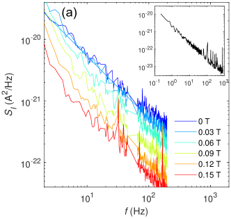
Fig. 2a displays measured noise power spectral density vs. frequency at a few fields between 0 and 0.15 T at 10 V using currents around . All the data are very close to the pure form: for the data at 0.03 T and , for example, fitting of a free exponent to yields . The inset displays a wider frequency scan of the noise at : clear noise is present over three decades in frequency. Our data also fulfill the basic properties of noise spectra as a function of bias current , where . The noise magnitude is approximately a constant, which is decomposed into and in our analysis. Compared with other low-noise graphene devices, the noise of our sample is on par with the lowest achieved results Kumar et al. (2015); Kamada et al. (2021b).
The noise changed irregularly with the increase of magnetic field at low temperatures, in particular at 4 K and below. This is assigned to the role of conductance fluctuations in our sample. Their significance becomes reduced with increasing temperature as the thermal diffusion length decreases from to about nm when is increased from 4 to 40 K. Consequently, we selected an operation temperature of K, at which the strength of individual conductance fluctuation features was sufficiently weakened, and the magnetic field dependence could be analyzed better in terms of diffusive transport models.
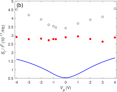
Charge density dependence of the scaled noise spectral density, and , where , is depicted in Fig. 2b for the graphene part and the contacts, respectively. The value for contact noise was determined from data measured at V in the unipolar regime where no interfaces exist and . The data points specified at Hz were taken from the fits of form to the measured spectra. The open circles denote the experimental data at 27 K, while the filled symbols and the blue curve indicate the separation between the noise contributions from the graphene itself and the contacts, respectively. Clearly, graphene contribution dominates the measured noise at the Dirac point, but at m-2 the graphene contacts account for of the noise. As the graphene resistance increases with , the contact contribution in the coupled noise becomes even less significant in a magnetic field. The dip structure in the noise near the Dirac point is due to the substantial magnitude of compared with the graphene noise, and it originates from the presence of both electron and hole carriers and incoherent addition of their contact noise contributions.
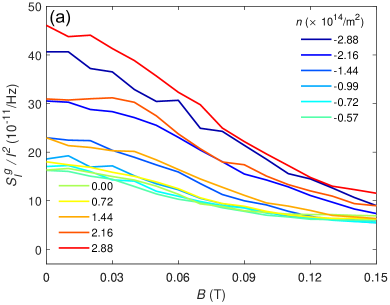
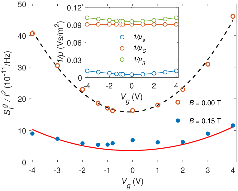
At small magnetic fields, T, the resistance grows as and, simultaneously, the apparent Dirac point shifts slightly higher in Kamada et al. (2021a). The magnetic field dependence of the measured noise is illustrated in Fig. 3a, which depicts scaled graphene noise power at 10 Hz as a function of magnetic field at several charge carrier densities near the Dirac point ( m-2). A clear reduction in noise is observed with increasing and the reduction takes place in approximately equal relative manner at all gate voltage values. The smallest noise is observed at the Dirac point, as typical, while the reduction of noise with becomes strongest at charge densities m-2 at which the reduction by the field amounts to . A leveling off of the reduction appears when approaching T, but no clear upturn is found in the investigated T range. T was selected as the upper limit in our analysis because there was already a deviation visible from the dependence in the magnetoresistance .
For Corbino devices with isotropic (scalar) mobility fluctuations , the current fluctuations should vanish at a sweet spot having . In practice, the sweet spot does not reduce the noise down to zero, but non-idealities/other noise sources will limit the reduction Levinshtein and Rumyantsev (1983); Song and Min (1985); Song et al. (1988); Orlov and Yakimov (1990); Rumyantsev et al. (2013). On the other hand, partial correlations between mobility fluctuations in radial and azimuthal direction may account for the observed noise reduction. If we simply calculate the total resistance fluctuations as a linear sum of local fluctuations of resistivity we obtain for total resistance fluctuations
| (4) |
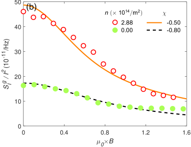
where we characterize the combined fluctuations of and by correlation coefficient according to ; similar formulas can be derived starting from anisotropic scattering Orlov (1992). When there is full positive (scalar) correlation (), the noise vanishes at . With full negative correlation , no suppression is seen in the noise Levinshtein and Rumyantsev (1983); Song and Min (1985); Song et al. (1988); Orlov and Yakimov (1990); Rumyantsev et al. (2013). By taking into account , our results in Fig. 3a yield away from the Dirac point. This result is in agreement with theoretical studies for changes in resistance due to reorganization of atoms Martin (1972); Nagaev and Kogan (1982),Orlov and Yakimov (1990) and also with noise correlation measurements in semimetallic Bi Black et al. (1983). According to our own kinetic Monte Carlo simulations (see Methods), the correlation coefficient is and for and at , respectively; here is the energy barrier for hopping between sites. The difference in these calculated values for can be explained by the fact that, at the lower temperature, a significant number of defects spend a considerable time at the electrodes forming elongated clusters instead of moving freely on graphene without additional restrictions on the shape of clusters as discussed in the supplementary information of Ref. Kamada et al., 2021b.
The gate voltage dependence of noise at and T is compared in Fig. 4. We observe that the difference between the data at and T grows monotonically when moving away from the Dirac point. The resistance fluctuations are increasingly suppressed from value with growing charge carrier density over m-2. This decrease can be assigned to a small change in the magnitude of correlations between and from (at Dirac point) to (at m-2). Possibly, the strengthening in anticorrelation between and is related to reduced screening at small charge densities.
Graphene properties may also become modified due to external factors, such as strain induced by or local strains induced by adsorption of adatoms Krasheninnikov and Nieminen (2011). According to Ref. Krasheninnikov and Nieminen, 2011, the stress field induced by the adatom extends over till the next nearest lattice sites and it involves asymmetry in the strain distribution. Such strain leads to pseudomagnetic fields Katsnelson (2012), which act as weak uniform scattering regions. In addition, there arises scalar (gauge) fields which may increase conductivity by enhancing local charge density Kamada et al. (2021b). Hence, adsorbed mobile atoms could provide short-ranged scattering centers which cause scalar-type mobility fluctuations, weakening negative correlations. Detailed theoretical modeling of the actual scattering centers and the ensuing is beyond the scope of the present work.
According to Eq. 2, graphene noise at varies as , where the scattering contribution due to mobile impurities, proportional to , may vary with gate voltage. Using diffusive transport theory Hwang et al. (2007); Kamada et al. (2021a), scattering by short range impurities produces while for Coulomb impurities , where and are constants. Using the mobility analysis described in Ref. Kamada et al., 2021a, we can determine , and . The division between relative scattering rates in terms of components and at 27 K is indicated in the inset of Fig. 4. If we assume that mobile impurities would be Coulomb scatterers with constant , would decrease with . Hence we conclude that the majority of mobile impurities in our device must be short range scatterers due to adatoms. For short-ranged scatterers, we obtain a parabolic change of upto % across the measured gate voltage range (see Fig. 4). This change will become reduced if part of the scatterers are Coulomb impurities. In fact, the adatoms will produce both short range scattering due to strain and long range scattering due to induced charge at the impurity site. Thus, the sharp division between short range and long range contributions is not properly valid for the mobile impurities present in our system. Nevertheless, the factor agrees with the functional form of the measured change, supporting the basic assumption of in our noise model. For better testing between theory and experiment, a separate means to determine the scattering contribution of the mobile impurities would be needed.
IV Conclusions
We have addressed the fundamental sources of noise in a low-noise, suspended graphene Corbino disk without strong two-level systems. By employing incoherent transport of electrons and holes, we could account for the contact noise by a single parameter. Also, we were able to account for the graphene noise, basically using a single parameter which is related to impurity movement and mobility fluctuations due to random agglomeration/deagglomeration of impurities. The noise decreased with increasing magnetic field, which pinpoints the nature of the noise to mobility fluctuations with intrinsic correlations between radial and azimuthal fluctuations. We find negative orthogonal mobility correlations, which agrees with expectations for ”rotating” impurities and our kinetic Monte Carlo simulations. With the significant noise suppression as a function of magnetic field, our work constitutes a strong direct demonstration of mobility noise in two dimensional materials.
Further work is needed to shed light on cluster formation of defects and collective dynamics of such clusters. Recent progress in both metallic and semiconducting 2D materials facilitates good opportunities in tackling these problems. The complex, and possibly self-limiting, dynamics of impurities provides a natural explanation for the long-time memory effects needed to create genuine noise, distinct from the regular noise theories based on distributed two-level or trap states. Our results demonstrate that these collective phenomena may be addressed in very clean micron scale systems.
Acknowledgements
We are grateful to Elisabetta Paladino, Igor Gornyi, Manohar Kumar, and Tapio Ala-Nissilä for fruitful discussions and to Sergey Rumyantsev for pointing Ref. Levinshtein and Rumyantsev, 1983 to us. This work was supported by the Academy of Finland projects 314448 (BOLOSE), 310086 (LTnoise) and 312295 (CoE, Quantum Technology Finland) as well as by ERC (grant no. 670743). The research leading to these results has received funding from the European Union’s Horizon 2020 Research and Innovation Programme, under Grant Agreement no 824109. The experimental work benefited from the Aalto University OtaNano/LTL infrastructure. A.L. is grateful to Väisälä foundation of the Finnish Academy of Science and Letters for scholarship.
Methods
All the suspended monolayer graphene devices employed in this work were fabricated using a technique based on lift off resist (LOR) sacrificial layer Tombros et al. (2011). Details on our sample fabrication process can be found in Ref. Kumar et al., 2018. First, graphene was exfoliated on LOR (thickness 500 nm) using a heat-assisted exfoliation technique Huang et al. (2015) and characterized using Raman spectroscopy. Electron-beam lithography was employed to pattern the contacts ( nm Cr/ nm Au) using a PMMA 50k/950k double layer resist. A global back gate was provided by the strongly doped silicon Si++ substrate with 285 nm of thermally grown SiO2 on it. Finally, the samples on LOR were current annealed at low temperatures, typically using a bias voltage of V. Most of the present work was performed on a Corbino disk with an area of and a distance of between the electrodes (inner and outer radii of 0.9 and , respectively); a scanning electron microscope picture of a similar Corbino sample is displayed in inset of Fig. 1. The gate capacitance F/m2 was obtained using filling factors of Landau levels Kumar et al. (2018).
In our experiments, we employed standard voltage-biased measurements for current fluctuations. The current was amplified using a transimpedance amplifier (SR570, gain ) and its fluctuations were measured using a Stanford Research SRS 785 FFT analyzer. For details of our experimental techniques we refer to Refs. Kumar et al., 2015; Laitinen et al., 2018.
Kinetic Monte Carlo (kMC) simulations were performed on a model system imitating the Corbino disk geometry by applying appropriate boundary conditions. The calculation procedure and assumptions are described in more detail in Ref. Kamada et al., 2021b. First, the trajectories of the defects on the Corbino disk were generated at two different temperatures ( and while energy barrier for hopping was ) by the kMC simulations allowing 25 defects to move via thermally activated diffusional hops on a 50 by 50 square lattice. The time evolution of the resistance was then calculated by finite element method (FEM) based on the output of the kMC describing the defect motion on the disk. As suggested by experiments with adsorbed Ne Kamada et al. (2021b), the defect sites were assumed to be more conductive than the background lattice. In the present model, the ratio of the conductivity values was set to . The FEM calculations were performed for the two orthogonal directions of the current flow, i.e. radial and azimuthal using the same kMC data in both. Finally, a correlation coefficient between the resistance fluctuations in the radial and azimuthal directions was calculated for the two different temperatures.
References
- Kogan (2008) S. Kogan, Electronic Noise and Fluctuations in Solids, 1st ed. (Cambridge University Press, New York, NY, USA, 2008).
- Grasser (2020) T. Grasser, Noise in Nanoscale Semiconductor Devices, edited by T. Grasser (Springer International Publishing, Cham, 2020) pp. 1–729.
- Hooge et al. (1981) F. N. Hooge, T. G. M. Kleinpenning, and L. K. J. Vandamme, Experimental studies on noise, Reports on Progress in Physics 44, 479 (1981).
- Hooge (1994) F. N. Hooge, noise sources, IEEE Transactions on Electron Devices 41, 1926 (1994).
- Feng et al. (1986) S. Feng, P. A. Lee, and A. D. Stone, Sensitivity of the conductance of a disordered metal to the motion of a single atom: Implications for noise, Physical Review Letters 56, 1960 (1986).
- Pelz and Clarke (1987) J. Pelz and J. Clarke, Quantitative ”local-interference” model for noise in metal films, Physical Review B 36, 4479 (1987).
- Ruseckas et al. (2011) J. Ruseckas, B. Kaulakys, and V. Gontis, Herding model and noise, EPL 96, 60007 (2011), arXiv:1111.1306 .
- Jensen (1990) H. J. Jensen, Lattice gas as a model of noise, Physical Review Letters 64, 3103 (1990).
- Ralls and Buhrman (1988) K. S. Ralls and R. A. Buhrman, Defect interactions and noise in metallic nanoconstrictions, Physical Review Letters 60, 2434 (1988).
- Balandin (2013) A. A. Balandin, Low-frequency noise in graphene devices., Nature Nanotechnology 8, 549 (2013), arXiv:1307.4797 .
- Karnatak et al. (2017) P. Karnatak, T. Paul, S. Islam, and A. Ghosh, noise in van der Waals materials and hybrids, Advances in Physics: X 2, 428 (2017).
- Heller et al. (2010) I. Heller, S. Chatoor, J. Männik, M. A. G. Zevenbergen, J. B. Oostinga, A. F. Morpurgo, C. Dekker, and S. G. Lemay, Charge noise in graphene transistors, Nano Letters 10, 1563 (2010).
- Pal et al. (2011) A. N. Pal, S. Ghatak, V. Kochat, E. S. Sneha, A. Sampathkumar, S. Raghavan, and A. Ghosh, Microscopic mechanism of noise in graphene: Role of energy band dispersion, ACS Nano 5, 2075 (2011).
- Zhang et al. (2011) Y. Zhang, E. E. Mendez, and X. Du, Mobility-dependent low-frequency noise in graphene field-effect transistors, ACS Nano 5, 8124 (2011).
- Kaverzin et al. (2012) A. A. Kaverzin, A. S. Mayorov, A. Shytov, and D. W. Horsell, Impurities as a source of noise in graphene, Physical Review B 85, 75435 (2012).
- Kumar et al. (2015) M. Kumar, A. Laitinen, D. Cox, and P. J. Hakonen, Ultra low noise in suspended bilayer graphene, Applied Physics Letters 106, 10.1063/1.4923190 (2015).
- Arnold et al. (2016) H. N. Arnold, V. K. Sangwan, S. W. Schmucker, C. D. Cress, K. A. Luck, A. L. Friedman, J. T. Robinson, T. J. Marks, and M. C. Hersam, Reducing flicker noise in chemical vapor deposition graphene field-effect transistors, Applied Physics Letters 108, 10.1063/1.4942468 (2016).
- Karnatak et al. (2016) P. Karnatak, T. P. Sai, S. Goswami, S. Ghatak, S. Kaushal, and A. Ghosh, Current crowding mediated large contact noise in graphene field-effect transistors, Nature Communications 7, 1 (2016).
- Pellegrini (2013) B. Pellegrini, noise in graphene, The European Physical Journal B 86, 373 (2013).
- Lu et al. (2014) J. Lu, J. Pan, S. S. Yeh, H. Zhang, Y. Zheng, Q. Chen, Z. Wang, B. Zhang, J. J. Lin, and P. Sheng, Negative correlation between charge carrier density and mobility fluctuations in graphene, Physical Review B 90, 085434 (2014).
- Dutta and Horn (1981) P. Dutta and P. M. Horn, Low-frequency fluctuations in solids: noise, Reviews of Modern Physics 53, 497 (1981).
- Orlov (1992) V. B. Orlov, Defect Motion as the Origin of the 1/f Conductance Noise in Solids, EUT report 92-E-25 (Eindhoven University of Technology, 1992).
- Levinshtein and Rumyantsev (1983) M. E. Levinshtein and S. L. Rumyantsev, Noise of the type under conditions of a strong geometric magnetoresistance, Soviet Physics: Semiconductors 17, 1167 (1983).
- Song and Min (1985) M. Song and H. S. Min, Influence of magnetic field on noise in GaAs Corbino disks, Journal of Applied Physics 58, 4221 (1985), https://doi.org/10.1063/1.335555 .
- Song et al. (1988) M. H. Song, A. N. Birbas, A. van der Ziel, and A. D. van Rheenen, Influence of magnetic field on noise in GaAs resistors without surface effects, Journal of Applied Physics 64, 727 (1988), https://doi.org/10.1063/1.341940 .
- Orlov and Yakimov (1990) V. Orlov and A. Yakimov, noise in Corbino disk: Anisotropic mobility fluctuations?, Solid State Electronics 33, 21 (1990).
- Rumyantsev et al. (2013) S. L. Rumyantsev, D. Coquillat, R. Ribeiro, M. Goiran, W. Knap, M. S. Shur, A. A. Balandin, and M. E. Levinshtein, The effect of a transverse magnetic field on noise in graphene, Applied Physics Letters 103, 173114 (2013), https://doi.org/10.1063/1.4826644 .
- Fleetwood (2015) D. M. Fleetwood, Noise and Defects in Microelectronic Materials and Devices, IEEE Transactions on Nuclear Science 62, 1462 (2015).
- Fleetwood and Giordano (1985) D. M. Fleetwood and N. Giordano, Direct link between noise and defects in metal films, Physical Review B 31, 1157 (1985).
- Hooge (1972) F. Hooge, Discussion of recent experiments on noise, Physica 60, 130 (1972).
- Kamada et al. (2021a) M. Kamada, V. Gall, J. Sarkar, M. Kumar, A. Laitinen, I. Gornyi, and P. Hakonen, Strong magnetoresistance in a graphene corbino disk at low magnetic fields, Physical Review B 104, 115432 (2021a).
- Xu et al. (2010) G. Xu, C. M. Torres, Y. Zhang, F. Liu, E. B. Song, M. Wang, Y. Zhou, C. Zeng, and K. L. Wang, Effect of spatial charge inhomogeneity on noise behavior in graphene, Nano Letters 10, 3312 (2010).
- Hwang et al. (2007) E. H. Hwang, S. Adam, and S. D. Sarma, Carrier transport in two-dimensional graphene layers, Physical Review Letters 98, 186806 (2007).
- Zheng and Ando (2002) Y. Zheng and T. Ando, Hall conductivity of a two-dimensional graphite system, Physical Review B 65, 245420 (2002).
- Müller et al. (2008) M. Müller, L. Fritz, and S. Sachdev, Quantum-critical relativistic magnetotransport in graphene, Physical Review B 78, 115406 (2008).
- Jobst et al. (2012) J. Jobst, D. Waldmann, I. V. Gornyi, A. D. Mirlin, and H. B. Weber, Electron-electron interaction in the magnetoresistance of graphene, Physical Review Letters 108, 106601 (2012).
- Alekseev et al. (2013) P. S. Alekseev, A. P. Dmitriev, I. V. Gornyi, and V. Y. Kachorovskii, Strong magnetoresistance of disordered graphene, Physical Review B 87, 165432 (2013).
- Kamada et al. (2021b) M. Kamada, A. Laitinen, W. Zeng, M. Will, J. Sarkar, K. Tappura, H. Seppä, and P. Hakonen, Electrical low-frequency noise due to surface diffusion of scatterers on an ultra-low-noise graphene platform, Nano Letters 21, 7637 (2021b), https://doi.org/10.1021/acs.nanoLetters1c02325 .
- Martin (1972) J. W. Martin, The electrical resistivity of some lattice defects in FCC metals observed in radiation damage experiments, Journal of Physics F: Metal Physics 2, 842 (1972).
- Nagaev and Kogan (1982) K. E. Nagaev and S. M. Kogan, Low-frequency current noise and internal friction in solids, Fiz. Tverd. Tela (Leningrad), Sov. Phys. Solid State 24, 1921 (1982).
- Black et al. (1983) R. D. Black, P. J. Restle, and M. B. Weissman, Nearly Traceless Noise in Bismuth, Physical Review Letters 51, 1476 (1983), arXiv:1011.1669v3 .
- Krasheninnikov and Nieminen (2011) A. V. Krasheninnikov and R. M. Nieminen, Attractive interaction between transition-metal atom impurities and vacancies in graphene: a first-principles study, Theoretical Chemistry Accounts 129, 625 (2011).
- Katsnelson (2012) M. I. Katsnelson, Graphene: Carbon in Two Dimensions (Cambridge University Press, 2012).
- Tombros et al. (2011) N. Tombros, A. Veligura, J. Junesch, J. J. van den Berg, P. J. Zomer, M. Wojtaszek, I. J. V. Marun, H. T. Jonkman, and B. J. van Wees, Large yield production of high mobility freely suspended graphene electronic devices on a polydimethylglutarimide based organic polymer, Journal of Applied Physics 109, 93702 (2011).
- Kumar et al. (2018) M. Kumar, A. Laitinen, and P. Hakonen, Unconventional fractional quantum Hall states and Wigner crystallization in suspended Corbino graphene, Nature Communications 9, 10.1038/s41467-018-05094-8 (2018), arXiv:1611.02742 .
- Huang et al. (2015) Y. Huang, E. Sutter, N. N. Shi, J. Zheng, T. Yang, D. Englund, H.-J. Gao, and P. Sutter, Reliable exfoliation of large-area high-quality flakes of graphene and other two-dimensional materials, ACS Nano 9, 10612 (2015).
- Laitinen et al. (2018) A. Laitinen, M. Kumar, T. Elo, Y. Liu, T. Abhilash, and P. Hakonen, Breakdown of Zero-Energy Quantum Hall State in Graphene in the Light of Current Fluctuations and Shot Noise, Journal of Low Temperature Physics 10.1007/s10909-018-1855-x (2018).