Observation of Aharonov-Bohm effect in PbTe nanowire networks
Abstract
We report phase coherent electron transport in PbTe nanowire networks with a loop geometry. Magneto-conductance shows Aharonov-Bohm (AB) oscillations with periods of and in flux. The amplitude of oscillations is enhanced near zero magnetic field, possibly due to interference between time-reversal paths. Temperature dependence of the AB amplitudes suggests a phase coherence length 8 - 12 m at 50 mK. This length scale is larger than the typical geometry of PbTe-based hybrid semiconductor-superconductor nanowire devices.
I Introduction
Topological quantum computing relies on braiding of Majorana zero modes (MZMs) to realize various quantum gate operations [1, 2]. A major theoretical proposal is the so-called measurement-based braiding where the topological qubit can be readout from interference between a MZM-involved path (electron ‘teleportation’) and a normal (topologically trivial) path [3, 4, 5, 6]. Therefore, phase coherent transport is a crucial ingredient in this roadmap. One-dimensional semiconductor-superconductor hybrid nanowire is a promising MZM candidate [7, 8, 9, 10] where the phase coherent transport can be revealed as Aharonov-Bohm (AB) oscillations in nanowire networks with a loop geometry. Among all 1D candidates, InSb and InAs nanowires are the mostly studied MZM material systems [11, 12, 13, 14, 15, 16], with AB effect demonstrated [17, 18, 19, 20, 21]. Recently, PbTe [22, 23, 24, 25, 26, 27] based nanowires [28, 29] have been proposed as a new MZM candidate [30]. In this paper, we report the observation of AB effect in PbTe nanowire networks.

II Device basics


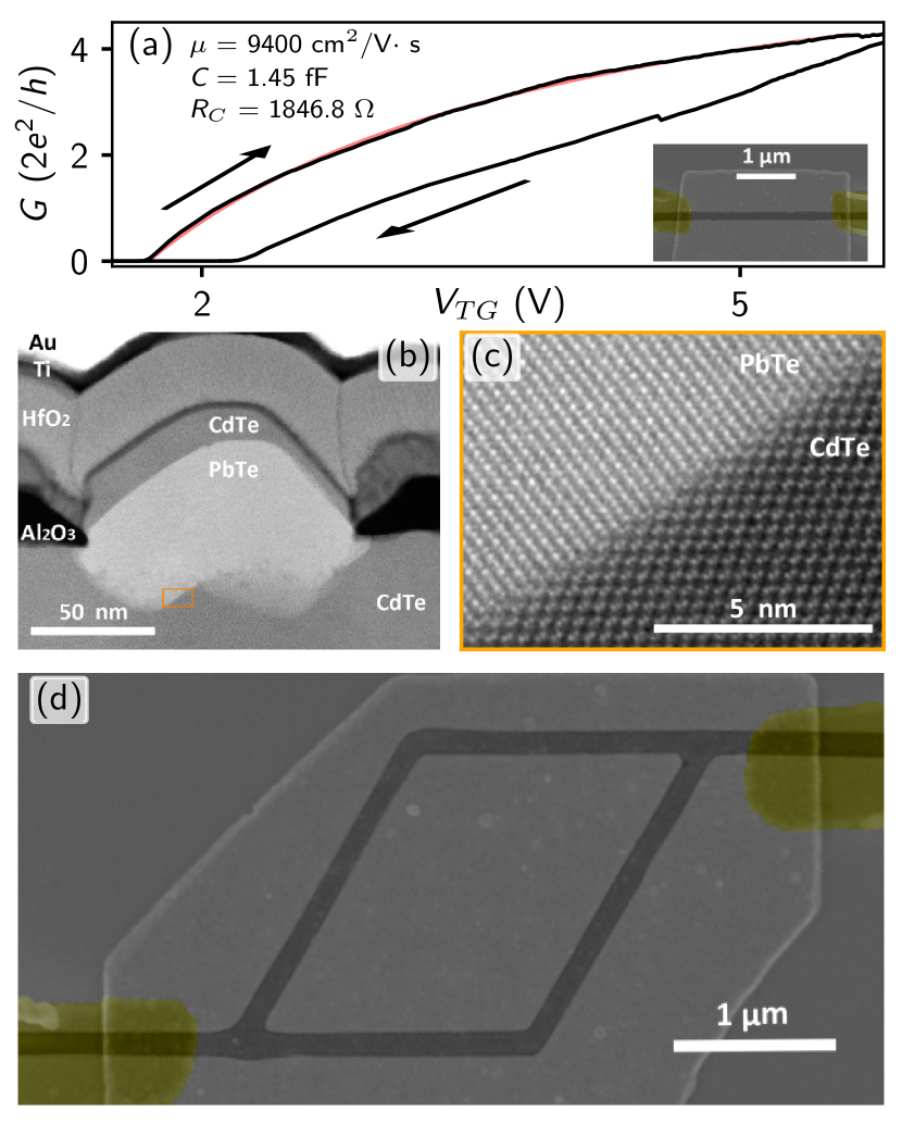
Fig. 1a (inset) shows the scanning electron micrograph (SEM) of a PbTe nanowire, selectively grown on a CdTe substrate using molecular beam epitaxy (MBE). The nanowire is contacted by two normal metal leads (yellow, Ti/Au) and then covered by a layer of HfO2 dielectric with a Ti/Au top gate. The selective area growth (SAG) of PbTe is achieved by covering the CdTe substrate with an Al2O3 dielectric mask followed by wet etched trenches. Growth details can be found in our recent work [29] where a CdTe(001) substrate was used. In this work, we choose a different substrate orientation, CdTe(111), for the PbTe growth. Valley-degeneracy breaking along this (111) direction, which is crucial in the realization of MZMs, has been experimentally demonstrated [25, 27] and theoretically verified [30].
Mobility fit (for the upward sweeping direction) of this field effect device (Fig. 1a) suggests a mobility 0.94 cm2/Vs, with the capacitance () estimated using a finite element model based on the device cross section (Fig. 1b). Clearly, the cross section has an irregular shape with rough interfaces, possibly due to the Ar treatment of the CdTe substrate before the PbTe growth. This interface can be a major source of disorder [31, 32, 33, 34, 35] and future growth optimization for flat interface may lead to higher mobility. Nevertheless, magnification of the interface (Fig. 1c) can still resolve matched lattices between PbTe and CdTe. Fig. 1d shows the SEM of a PbTe network device (Device A), grown and fabricated (contact, dielectric and gate) together with the mobility device on the same substrate chip. Transmission electron microscopy (TEM) analysis of Device A can be found in Supplementary (Sfig. 1).
III AB oscillations in Device A
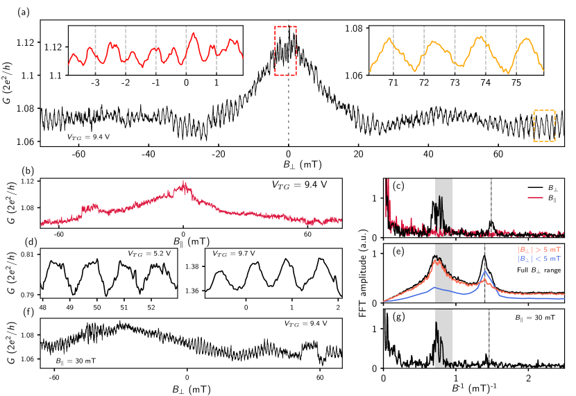
Fig. 2a shows the magneto-conductance of Device A, measured in a dilution refrigerator with a base temperature 20 mK. The differential conductance was measured using a lock-in amplifier in a two terminal circuit set-up. The bias voltage was fixed at zero throughout the measurement. The magnetic field () was oriented perpendicular to the substrate for Fig. 2a. The overall conductance shows a peak near = 0 T, suggesting the existence of weak anti-localization (WAL). On top of the background, periodic AB oscillations are resolved with periods of 1.4 mT (orange inset) and 0.7 mT (red inset), corresponding to flux periods of (first harmonic) and (second harmonic), respectively. Here, is the Plank constant and the electron charge. We further convert this period in into an effective loop area 2.95 m2 based on the formula of . This extracted area is close to the area defined by the inner surface of the nanowire loop ( 2.9 m2), suggesting that the electron wave-function is mainly distributed near the inner surface.
For a control test, we also apply parallel to the substrate and observe a WAL peak without AB oscillations (Fig. 2b). In Fig. 2c we plot the spectrum of Fast Fourier Transform (FFT) where the and oscillations in Fig. 2a are revealed as two FFT peaks (black curve). By contrast, the FFT of Fig. 2b shows no such peaks (the red curve in Fig. 2c). Boundaries of the shaded area refer to the expected AB periods estimated based on the area encircled by the inner and outer surfaces of the nanowire loop. The dashed line is the expected peak position of the second harmonic (), calculated by multiplying the center of the first harmonic peak by a factor of two.
We further show the magneto-conductance of Device A at different gate voltages, see supplementary (Sfig. 2). The AB amplitude varies for different gate voltages, as well as for the same gate voltage but repeated measurements, possibly due to device instabilities. In some gate settings, we observe no AB oscillations, possibility due to the pinch-off of one of the two AB ‘arms’ or other unknown dephasing mechanisms. Fig. 2d shows examples for and oscillations with amplitudes reaching 0.015 and 0.02, in unit of . In Fig. 2e we show the ensemble averaged FFT for all (in total 182 sets) measured -sweeping curves (the black line), where the first and second harmonic peaks are clearly visible. The second harmonic peak has a similar height as the first one, suggesting a significant -component. The oscillations in Fig. 2a are mostly prominent near = 0 T, possibly due to the time-reversal paths. To confirm this hypothesis, we perform the ensemble averaged FFT for near 0 T (blue curve in Fig. 2e) which indeed resolves a more prominent peak. By contrast, the averaged FFT for higher resolves a much smaller peak (red curve in Fig. 2e). In addition, in Fig. 2f with a small fixed in-plane magnetic field of 30 mT, the out-of-plane magneto-conductance reveals mainly the oscillations even for out-of-plane near 0 T. The corresponding FFT (Fig. 2g) also confirms that the peak is hardly visible.
IV Temperature Dependence
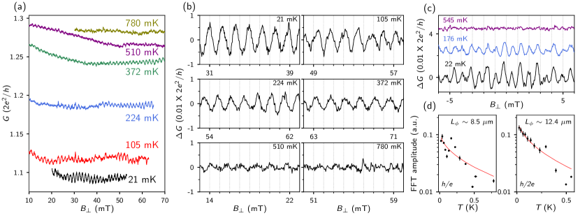
We now study the temperature dependence of the AB oscillations. Fig. 3a shows the oscillations with temperatures vary from 21 mK to 780 mK (only six curves are shown for clarity). The -evolution of AB amplitudes is more visible after subtracting an overall background (by smoothing the curve), as shown in Fig. 3b which focuses on the -ranges with large oscillations. The oscillation amplitude is reduced by roughly half at 200 - 300 mK, and almost vanishes at 780 mK. Fig. 3c shows the oscillation (background subtracted) at three typical s, resolving similar trend.

To quantify the and oscillation amplitudes, we perform FFT and estimate the amplitude by the ‘area’ underneath the corresponding FFT peak. This area is calculated by numerical integration, see Sfig. 3 for detailed information. Fig. 3d shows (left) and (right) amplitudes decaying with increasing as a general trend. The fluctuations is possibly due to instabilities within the mesoscopic environment. To fit this decay, we adopt a diffusive transport model [36, 20], where the AB amplitude is assumed to be and assumed to be . is the phase coherence length and is one half of the loop circumference for and the full circumference for oscillations. The fitting result (red lines in Fig. 3d) suggests a phase coherence length 8 - 12 m at a temperature of 50 mK. We note this value is only a rough estimation which may vary for different models. The extracted length scale (a few micron) is consistent with the observation of oscillations: electrons remain phase coherent after circulating the whole loop which is 8 m.
V AB oscillations in another Device
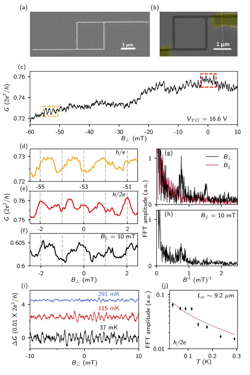
Finally, we show AB oscillations observed in a second device (Device B). The loop geometry has a square shape instead of a diamond as shown in Fig. 4a-b. The magneto-conductance (Fig. 4c) resolves AB oscillations with period near zero and period at higher , see Fig. 4d-e for the magnifications with corresponding colors. The AB periods for and oscillations are 1.25 and 0.66 mT, respectively. This period in can be converted into an effective loop area of 3.3 m2. Based on the device SEM, we can independently estimate the loop area to be 3 and 4 m2 for the inner and outer surfaces, respectively. Comparison to the evaluated loop area again suggests that the electrons are mainly located near the inner surface of the loop.
Fig. 4g shows the FFT of Fig. 4c, resolving the two harmonic peaks (black curve). As a comparison, FFT of a -scan curve (not shown), measured under the same gate voltage but with parallel to the substrate, resolves no such peaks (red curve). The oscillations are also enhanced near zero , similar to the case in Device A. This component can be reduced by a fixed in-plane of 10 mT, as shown in Fig. 4f. The corresponding FFT (for the whole range) also only resolves the peak (Fig. 4h).
Due to the device instabilities, we have only performed temperature dependence for the oscillations, see Fig. 4i for the oscillations at three different temperatures. In Fig. 4j, we plot the FFT amplitudes vs temperature, fit the diffusive transport model and extract the phase coherence length m at = 50 mK. This result is roughly consistent with the value of Device A. For more -scans of Device B, see Sfig. 2.
VI Summary
To summarize, we have demonstrated phase coherent transport in PbTe nanowire networks by observing Aharonov-Bohm oscillations in magneto-conductance. Both - and -period oscillations can be revealed. Temperature dependence of the AB amplitude suggests a phase coherence length 8 - 12 m at = 50 mK. This length scale exceeds the dimension of future PbTe-based hybrid semiconductor-superconductor devices, fulfilling a necessary condition for the exploration of topological quantum information processing. Future works could be aiming at the optimization of the nanowire growth for more uniform cross-sections which may lead to higher mobility and longer phase coherence length.
VII Acknowledgment
We thank Gu Zhang and Zhan Cao for valuable discussions. This work is supported by Tsinghua University Initiative Scientific Research Program, National Natural Science Foundation of China (92065206, 51788104) and National Key Research and Development Program of China (2017YFA0303303). Raw data and processing codes within this paper are available at https://zenodo.org/record/5798424.
References
- Kitaev [2003] A. Kitaev, Fault-tolerant quantum computation by anyons, Annals of Physics 303, 2 (2003).
- Nayak et al. [2008] C. Nayak, S. H. Simon, A. Stern, M. Freedman, and S. Das Sarma, Non-abelian anyons and topological quantum computation, Rev. Mod. Phys. 80, 1083 (2008).
- Fu [2010] L. Fu, Electron teleportation via majorana bound states in a mesoscopic superconductor, Phys. Rev. Lett. 104, 056402 (2010).
- Plugge et al. [2017] S. Plugge, A. Rasmussen, R. Egger, and K. Flensberg, Majorana box qubits, New Journal of Physics 19, 012001 (2017).
- Vijay and Fu [2016] S. Vijay and L. Fu, Teleportation-based quantum information processing with majorana zero modes, Phys. Rev. B 94, 235446 (2016).
- Karzig et al. [2017] T. Karzig, C. Knapp, R. M. Lutchyn, P. Bonderson, M. B. Hastings, C. Nayak, J. Alicea, K. Flensberg, S. Plugge, Y. Oreg, C. M. Marcus, and M. H. Freedman, Scalable designs for quasiparticle-poisoning-protected topological quantum computation with majorana zero modes, Phys. Rev. B 95, 235305 (2017).
- Lutchyn et al. [2010] R. M. Lutchyn, J. D. Sau, and S. Das Sarma, Majorana fermions and a topological phase transition in semiconductor-superconductor heterostructures, Phys. Rev. Lett. 105, 077001 (2010).
- Oreg et al. [2010] Y. Oreg, G. Refael, and F. von Oppen, Helical liquids and majorana bound states in quantum wires, Phys. Rev. Lett. 105, 177002 (2010).
- Prada et al. [2020] E. Prada, P. San-Jose, M. W. de Moor, A. Geresdi, E. J. Lee, J. Klinovaja, D. Loss, J. Nygård, R. Aguado, and L. P. Kouwenhoven, From andreev to majorana bound states in hybrid superconductor–semiconductor nanowires, Nature Reviews Physics 2, 575 (2020).
- Zhang et al. [2019] H. Zhang, D. E. Liu, M. Wimmer, and L. P. Kouwenhoven, Next steps of quantum transport in majorana nanowire devices, Nature Communications 10, 1 (2019).
- Mourik et al. [2012] V. Mourik, K. Zuo, S. M. Frolov, S. Plissard, E. P. Bakkers, and L. P. Kouwenhoven, Signatures of majorana fermions in hybrid superconductor-semiconductor nanowire devices, Science 336, 1003 (2012).
- Deng et al. [2016] M. Deng, S. Vaitiekėnas, E. B. Hansen, J. Danon, M. Leijnse, K. Flensberg, J. Nygård, P. Krogstrup, and C. M. Marcus, Majorana bound state in a coupled quantum-dot hybrid-nanowire system, Science 354, 1557 (2016).
- Albrecht et al. [2016] S. M. Albrecht, A. P. Higginbotham, M. Madsen, F. Kuemmeth, T. S. Jespersen, J. Nygård, P. Krogstrup, and C. Marcus, Exponential protection of zero modes in majorana islands, Nature 531, 206 (2016).
- Gül et al. [2018] Ö. Gül, H. Zhang, J. D. Bommer, M. W. de Moor, D. Car, S. R. Plissard, E. P. Bakkers, A. Geresdi, K. Watanabe, T. Taniguchi, et al., Ballistic majorana nanowire devices, Nature Nanotechnology 13, 192 (2018).
- Zhang et al. [2021] H. Zhang, M. W. de Moor, J. D. Bommer, D. Xu, G. Wang, N. van Loo, C.-X. Liu, S. Gazibegovic, J. A. Logan, D. Car, R. L. M. Op het Veld, P. J. van Veldhoven, S. Koellinga, M. A. Verheijen, M. Pendharkar, D. J. Pennachio, B. Shojaei, J. S. Lee, C. J. Palmstrøm, E. P. Bakkers, S. Das Sarma, and L. P. Kouwenhoven, Large zero-bias peaks in insb-al hybrid semiconductor-superconductor nanowire devices, arXiv: 2101.11456 (2021).
- Song et al. [2021] H. Song, Z. Zhang, D. Pan, D. Liu, Z. Wang, Z. Cao, L. Liu, L. Wen, D. Liao, R. Zhuo, D. E. Liu, R. Shang, J. Zhao, and H. Zhang, Large zero bias peaks and dips in a four-terminal thin inas-al nanowire device, arXiv: 2107.08282 (2021).
- Gazibegovic et al. [2017] S. Gazibegovic, D. Car, H. Zhang, S. C. Balk, J. A. Logan, M. W. de Moor, M. C. Cassidy, R. Schmits, D. Xu, G. Wang, et al., Epitaxy of advanced nanowire quantum devices, Nature 548, 434 (2017).
- Vaitiekėnas et al. [2018] S. Vaitiekėnas, A. M. Whiticar, M.-T. Deng, F. Krizek, J. E. Sestoft, C. J. Palmstrøm, S. Marti-Sanchez, J. Arbiol, P. Krogstrup, L. Casparis, and C. M. Marcus, Selective-area-grown semiconductor-superconductor hybrids: A basis for topological networks, Phys. Rev. Lett. 121, 147701 (2018).
- Lee et al. [2019] J. S. Lee, S. Choi, M. Pendharkar, D. J. Pennachio, B. Markman, M. Seas, S. Koelling, M. A. Verheijen, L. Casparis, K. D. Petersson, I. Petkovic, V. Schaller, M. J. W. Rodwell, C. M. Marcus, P. Krogstrup, L. P. Kouwenhoven, E. P. A. M. Bakkers, and C. J. Palmstrøm, Selective-area chemical beam epitaxy of in-plane inas one-dimensional channels grown on inp(001), inp(111)b, and inp(011) surfaces, Phys. Rev. Materials 3, 084606 (2019).
- Aseev et al. [2019] P. Aseev, G. Wang, L. Binci, A. Singh, S. Martí-Sánchez, M. Botifoll, L. J. Stek, A. Bordin, J. D. Watson, F. Boekhout, et al., Ballistic insb nanowires and networks via metal-sown selective area growth, Nano letters 19, 9102 (2019).
- het Veld et al. [2020] R. L. O. het Veld, D. Xu, V. Schaller, M. A. Verheijen, S. M. Peters, J. Jung, C. Tong, Q. Wang, M. W. de Moor, B. Hesselmann, et al., In-plane selective area insb–al nanowire quantum networks, Communications Physics 3, 1 (2020).
- Springholz et al. [1993] G. Springholz, G. Ihninger, G. Bauer, M. Olver, J. Pastalan, S. Romaine, and B. Goldberg, Modulation doping and observation of the integral quantum hall effect in pbte/pb1- x eu x te multiquantum wells, Applied physics letters 63, 2908 (1993).
- Grabecki et al. [1999] G. Grabecki, J. Wróbel, T. Dietl, K. Byczuk, E. Papis, E. Kamińska, A. Piotrowska, G. Springholz, M. Pinczolits, and G. Bauer, Quantum ballistic transport in constrictions of n-pbte, Physical Review B 60, R5133 (1999).
- Grabecki et al. [2004] G. Grabecki, J. Wrobel, T. Dietl, E. Papis, E. Kamińska, A. Piotrowska, A. Ratuszna, G. Springholz, and G. Bauer, Ballistic transport in pbte-based nanostructures, Physica E: Low-dimensional Systems and Nanostructures 20, 236 (2004).
- Grabecki et al. [2005] G. Grabecki, J. Wróbel, T. Dietl, E. Janik, M. Aleszkiewicz, E. Papis, E. Kamińska, A. Piotrowska, G. Springholz, and G. Bauer, Disorder suppression and precise conductance quantization in constrictions of pbte quantum wells, Phys. Rev. B 72, 125332 (2005).
- Chitta et al. [2006] V. Chitta, W. Desrat, D. Maude, B. Piot, N. Oliveira Jr, P. Rappl, A. Ueta, and E. Abramof, Integer quantum hall effect in a pbte quantum well, Physica E: Low-dimensional Systems and Nanostructures 34, 124 (2006).
- Grabecki et al. [2006] G. Grabecki, J. Wróbel, T. Dietl, E. Janik, M. Aleszkiewicz, E. Papis, E. Kamińska, A. Piotrowska, G. Springholz, and G. Bauer, Pbte—a new medium for quantum ballistic devices, Physica E: Low-dimensional Systems and Nanostructures 34, 560 (2006).
- Schellingerhout et al. [2021] S. Schellingerhout, E. de Jong, M. Gomanko, X. Guan, Y. Jiang, M. Hoskam, S. Koelling, O. Moutanabbir, M. Verheijen, S. Frolov, and E. Bakkers, Growth of pbte nanowires by molecular beam epitaxy, arXiv:2110.12789 (2021).
- Jiang et al. [2021] Y. Jiang, S. Yang, L. Li, W. Song, W. Miao, B. Tong, Z. Geng, Y. Gao, R. Li, Q. Zhang, et al., Selective area epitaxy of pbte-pb hybrid nanowires on a lattice-matched substrate, arXiv preprint arXiv:2110.13642 (2021).
- Cao et al. [2021] Z. Cao, D. E. Liu, W.-X. He, X. Liu, K. He, and H. Zhang, Numerical study of pbte-pb hybrid nanowires for engineering majorana zero modes, arXiv preprint arXiv:2110.13803 (2021).
- Pan and Das Sarma [2020] H. Pan and S. Das Sarma, Physical mechanisms for zero-bias conductance peaks in majorana nanowires, Phys. Rev. Research 2, 013377 (2020).
- Das Sarma and Pan [2021] S. Das Sarma and H. Pan, Disorder-induced zero-bias peaks in majorana nanowires, Phys. Rev. B 103, 195158 (2021).
- Zeng et al. [2021] C. Zeng, G. Sharma, S. Tewari, and T. Stanescu, Partially-separated majorana modes in a disordered medium, arXiv: 2105.06469 (2021).
- Ahn et al. [2021] S. Ahn, H. Pan, B. Woods, T. D. Stanescu, and S. Das Sarma, Estimating disorder and its adverse effects in semiconductor majorana nanowires, Phys. Rev. Materials 5, 124602 (2021).
- Woods et al. [2021] B. D. Woods, S. Das Sarma, and T. D. Stanescu, Charge-impurity effects in hybrid majorana nanowires, Phys. Rev. Applied 16, 054053 (2021).
- Kurdak et al. [1992] C. Kurdak, A. M. Chang, A. Chin, and T. Y. Chang, Quantum interference effects and spin-orbit interaction in quasi-one-dimensional wires and rings, Phys. Rev. B 46, 6846 (1992).