Intercalation of Mn in graphene/Cu(111) interface: Insights to the electronic and magnetic properties from theory
Abstract
The effect of Mn intercalation on the atomic, electronic and magnetic structure of the graphene/Cu(111) interface is studied using state-of-the-art density functional theory calculations. Different structural models of the graphene-Mn-Cu(111) interface are investigated. While a Mn monolayer placed between graphene and Cu(111) (an unfavorable configuration) yields massive rearrangement of the graphene-derived bands in the vicinity of the Fermi level, the possible formation of a Cu2Mn alloy at the interface (a favorable configuration) preserves the linear dispersion for these bands. The deep analysis of the electronic states around the Dirac point for the graphene/Cu2Mn/Cu(111) system allows to discriminate between contributions from three carbon sublattices of a graphene graphene layer in this system and to explain the bands’ as well as spins’ topology of the electronic states around the Fermi level.
SHU] Department of Physics, Shanghai University, Shangda Road 99, 200444 Shanghai, China SHU] Department of Physics, Shanghai University, Shangda Road 99, 200444 Shanghai, China SHU] Department of Physics, Shanghai University, Shangda Road 99, 200444 Shanghai, China
1 Introduction
Since the discovery of the unique properties of graphene 1, many fascinating phenomena in this material were demonstrated, exemplified by massless Dirac fermion physics 2, 3, 4, an anomalous quantum Hall effect 5, 6, 7, 8, and superconductivity 9. As an ideal 2D material, graphene has many possible attractive practical applications, such as protective coatings 10, touch screens 11, 12, gas sensors 13 and many others. With respect to the graphene-metal systems, the synthesis of graphene on metals is considered as one of the most promising technological approach 11, with further processing of the obtained graphene layers. Moreover, the graphene-metal interfaces, particularly graphene-ferromagnet, are proposed for the realization of the spintronics applications based on the transport of electrical charge or/and spin, such as the spin filters 14 and stable spin emitters 15, 16. Therefore, the understanding of the crystallographic structure and electronic properties of such graphene-metal interfaces 17, 18 is an initial prerequisite for the further studies of these systems.
From the point of view of electronic structure, graphene adsorbed on metal surfaces shows two distinct cases 19: (1) in the weakly bonded case, graphene is always doped (-type or -type), while the electronic structure characteristic for freestanding graphene remains almost intact [examples: graphene/Ir(111) 20, graphene/Pt(111) 21, graphene/Al(111) 22, and graphene/Cu(111) 23] and (2) in the strongly bonded case, graphene overlayer demonstrates the significant distortion of the linear dispersion relation for the graphene bands due to the strong overlap of the graphene states and valence band states of the underlying materials (space, energy, and -vector overlapping), that leads to the complete disappearance of the Dirac point in graphene [examples: graphene/Ni(111) 24, graphene/Co(0001) 25, graphene/Ru(0001) 26].
The electronic structure of graphene on metals can be altered in different ways, like intercalation of different species in graphene/metal interfaces, adsorption of atoms or molecules on top of graphene, graphene’s edge engineering, creation of the graphene nanostructures, etc. It is well known that the intercalation between graphene and metallic substrates can strongly affects the properties of the graphene-metal interface. There are several possible results of this process: (1) The intercalated species may decouple graphene from strongly interacting substrates, such as in the case of graphene/Al/Ni(111) 27, 28, graphene/Au/Ni(111) 29 and graphene/Cu/Ni(111) 30; (2) Such intercalated layers lead to the change the carrier concentration in graphene, and even change the carrier type (from holes to electrons) such as in the case of Cu intercalation in graphene/Ir(111) 31; (3) Intercalated metals may also enhance the magnetic coupling between a ferromagnetic substrate and graphene, such as graphene/Fe/Ni(111) 32 and graphene/Ni3Mn/Ni(111) 33, which improves the possible spin-filtering properties of graphene; (4) The intercalated layer in itself may bring new properties to graphene, such as in the case of intercalated lithium, where superconductivity in graphene has been predicted to occur 34.
Considering that graphene can be synthesized on Cu foil and the electronic properties of weakly-bonded graphene on Cu(111) has been well studied, the intercalation of Mn atoms (which possess the high magnetic moment due to the half-filled -shell, Mn ) in the graphene/Cu(111) system could be an interesting way to tailor the electronic and magnetic properties of graphene. Here, we present systematic structural and electronic properties studies of the system formed after intercalation of Mn in the graphene/Cu(111) interfaces using the density functional theory (DFT). It is found that the intercalation of a monolayer of Mn and formation of the sharp graphene/Mn/Cu(111) interface changes the electronic properties of graphene greatly, while the formation of the Cu2Mn interface alloy on Cu(111) only makes graphene -doped and leaves the linear dispersion of the graphene-derived states at the Fermi level (), which is similar to the case of graphene on Cu(111). The magnetic properties of the obtained interfaces and their possible application in graphene-based spin filtering devices are discussed in details.
2 Results and discussion
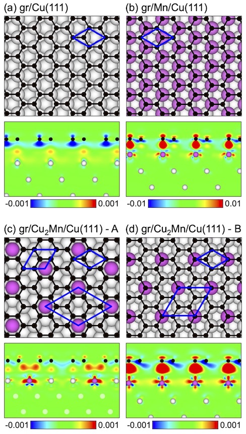
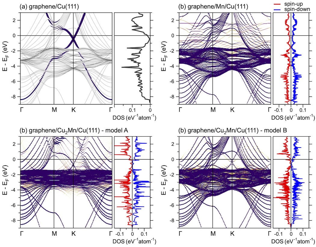
We first discuss the structural and electronic properties of graphene grown on Cu(111) as a reference system. When studying the interface between graphene and close-packed metal surface, three “high-symmetry” structures, which preserve symmetry, known as top–fcc (TF), top–hcp (TH), and fcc–hcp (FH) are usually considered 35 (for details, see Supplementary information, Fig. S1 and Tab. S1). According to our calculations, the TF structure for graphene/Cu(111), schematically shown in Fig. 1(a), was found to be the energetically most stable one. The results of our calculations for this structure are summarized in Tab. 1. Here, the graphene interaction energy of meV/C-atom and the distance of Å between graphene and top layer of the Cu(111) slab are indication of the weak interaction between graphene and the substrate. Nevertheless, as discussed below, it yields noticeable modifications of the graphene and copper band structures.
For the clean metal surface, Cu(111), the well-known -gap surface state around the -point is found in ARPES experiments 36. Using the graphene’s lattice constant, the calculated binding energy of this state at the -point is meV. [Note: A strong deviation from the experimental binding energy is due to the compression of Cu(111) lattice parameters. Complete relaxation of coordinates leads to the in-plane lattice constant of Cu(111) of Å and to the significant improvement of agreement between theory ( meV) and experiment ( meV 36)]. In our calculations for graphene/Cu(111) we detect the upward energy shift of the metal surface state by meV compared to clean Cu(111). This effect, observed earlier also for the adsorption of graphene on Ag(111) and Au(111) surfaces 37, 38, can be explained by the stronger localization of the metal surface state wave-function upon physisorption of graphene on Cu(111) compared to the clean Cu surface. There is also a charge transfer from the Cu(111) surface to graphene (Fig. 1(a)). As a result, graphene became -doped with the position of the Dirac point at meV (Fig. 2(a)), which is consistent with the previously published results for graphene/Cu(111) 39, 40. Closer look at the calculated band structure of graphene/Cu(111) allows to detect hybridization between the Cu and graphene states in the energy range of eV and consequent opening of the energy gap of meV directly at 39.
When discussing intercalation of Mn under graphene on Cu(111), several scenario are possible. Let us start with an assumption that Mn atoms form a 2D hexagonal layer commensurated with the ()-Cu(111) substrate. Here, Mn intercalant can occupy either fcc hollow or hcp hollow sites above Cu(111). Together with already mentioned three high-symmetry structures for graphene on Cu(111), this results in structural possibilities (for details, see Supplementary information, Fig. S2 and Tab. S2). Besides two possible magnetic orders for Mn atoms – ferromagnetic (FM) and row-wise antiferromagnetic (AFM) – have to be taken into account. The energetically most stable structure according to our calculations corresponds to the case where graphene keeps its TF arrangement with respect to Cu(111) and intercalated Mn occupies the fcc hollow sites above Cu(111) (Fig. 1(b)). The magnetic moments of Mn atoms () are coupled antiferromagnetically. The results of our calculations for this structure are summarized in Tab. 1. Intercalation of Mn yields the increase of the interaction energy between graphene and metal ( meV/C-atom). This is reflected by the decreased distance between graphene and Mn/Cu(111) ( Å), which allows for a strong hybridization between graphene and Mn valence bands states resulting in destruction of the Dirac cone (Fig. 2(b)). The magnetic moment of Mn atoms are , while the induced magnetic moments of carbon atoms in graphene overlayer are and , which are detectable in magnetic spectroscopic experiments.
According to available experimental and theoretical data, epitaxial Mn films grown on Cu(111) form a surface alloy Cu2Mn having a superstructure with respect to Cu(111) 41, 42. Graphene adsorbed on superstructured Mn-Cu(111) surface was previously investigated by means of DFT in the studies on the grain boundaries suppression during the graphene growth 43. In this work the energetically most stable arrangement corresponds to the structure shown in Fig. 1(c) (model A). Here, both monolayers – the Cu2Mn alloy and the graphene layer – are rotated by with respect to Cu(111). From experimental point of view, the existence of such a structure is hardly possible. Indeed, the preparation of graphene on Mn-Cu(111) is a two-step procedure. Firstly, graphene is synthesized on single crystal Cu(111) by thermal decomposition of, e. g., ethylene (C2H4) in an ultrahigh vacuum chamber. As a result, the lattices of graphene and Cu(111) are aligned in the same direction (with a possible formation of the moiré structure due to the lattice mismatch between two materials) 44. On the second step, the annealing of the prediposited Mn leads to intercalation of Mn with a formation of system, which is supposed to be an ordered graphene/Cu2Mn/Cu(111) trilayer. In such a procedure, it is difficult to expect any change of the graphene orientation (rotation) with respect to the Cu(111) surface. Thus, in our studies, when considering the formation of a Cu2Mn surface alloy at the graphene/Cu(111) interface, the related orientation between graphene and Cu(111) was kept unchanged, while a superstructure of Cu2Mn with respect to the both Cu(111) and graphene was preserved. For comparison reasons we have considered different high-symmetry arrangements of graphene above the Cu2Mn/Cu(111) substrate and two possible magnetic orders for Mn atoms (for details, see Supplementary information, Tab. S3 and Fig. S3). The energetically most stable structure – TH – is shown in Fig. 1(d) (model B). Here the magnetic moments of Mn atoms are coupled ferromagnetically and the TH and TF arrangements of C-atoms are energetically degenerate with the difference in the total energy of only meV (see Tab. S3). The calculations for the previously reported structure 43 shown in Fig. 1(c) (model A) are also performed for comparison reasons. The results are summarized in Tab. 1.
For the both structures under consideration (model A and model B), the calculated interaction energy between graphene and Cu2Mn/Cu(111) as well as the equilibrium distance between graphene and substrate are close to the values obtained for graphene/Cu(111). In both cases graphene is strongly -doped due to the charge transfer from the metal to graphene valence band states (Fig. 1(c,d)). In both structures, Mn atoms possess quite substantial magnetic moment – and for model A and model B, respectively (Tab. 1). However, the induced magnetic moment in a graphene layer does not exceed the value of for carbon atoms adsorbed above Mn atoms and they are coupled antiferromagnetically with respect to those of metal ions.
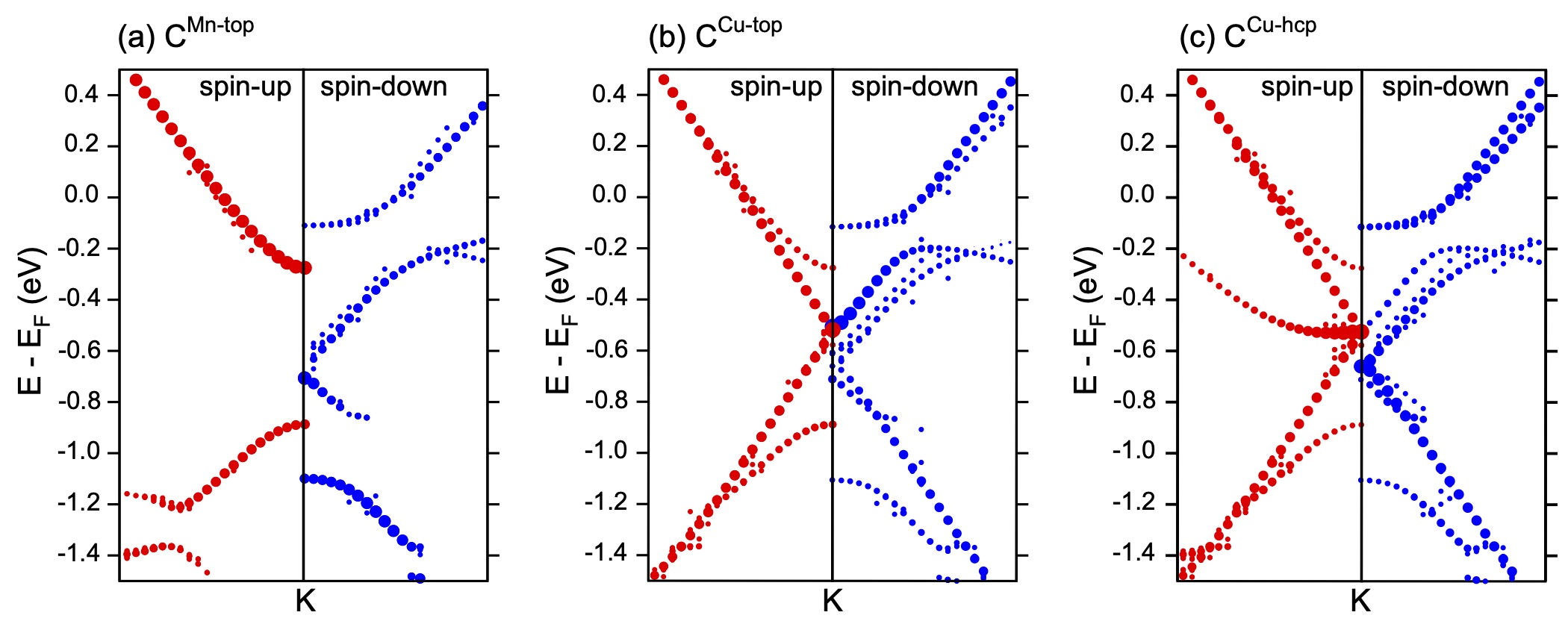
The calculated band structures (only for spin-up channel) are shown in Fig. 2(c) and Fig. 2(d) for model A and model B, respectively (see also Fig. S4 for complete spin-resolved band structures). Fig. 3(a-c) also shows the zoomed region around the point for the most energetically stable configuration of the graphene/Cu2Mn/Cu(111) system in model B for spin-up and spin-down channels, respectively. This figure represents the decomposition of the respective spin channels for graphene states around the point on the C-atoms projected weights corresponding to different carbon atoms in the unit cell of the graphene/Cu2Mn/Cu(111) – model B structure. From the presented data, it is clear that the existence of three different adsorption sites of carbon atoms in the unit cell for this structure leads to the respective splitting of the graphene band around the point in to three band’s branches. For the first one, associated with the carbon atoms above the Cu-hcp atoms of the Cu(111) slab (Fig. 3(a)), the linear dispersion of the graphene states is still conserved (although it is spin split) allowing to estimate the doping level of graphene and obtain the position of the Dirac points eV and eV for spin-up and spin-down channels, respectively. For carbon atoms adsorbed above the Cu-top atoms of the Cu2Mn layer (Fig. 3(b)), the linear dispersion is preserved only for spin-up channel and band gap at the Dirac point is opened for the spin-down channel. The most disturbed bands dispersions are found for the graphene bands branches associated with the carbon atoms above the Mn-top atoms of the Cu2Mn layer (Fig. 3(c)). The significant spin splitting of the bands of eV in the later case can be assigned to the appearance of the corresponding magnetic moments of carbon atoms adsorbed above the Mn atoms, which have large magnetic moment. The respective energy splitting of the bands and formation of the band gap for these graphene bands branches can be associated with the hybridization of the graphene and Mn states (, , ). The observed misbalance at the Fermi level of the respective weights for different spin channels of the graphene states might lead to the different conductivity for spin-up and spin-down channels, which could be useful in future spintronics applications and can be a topic for further studies.
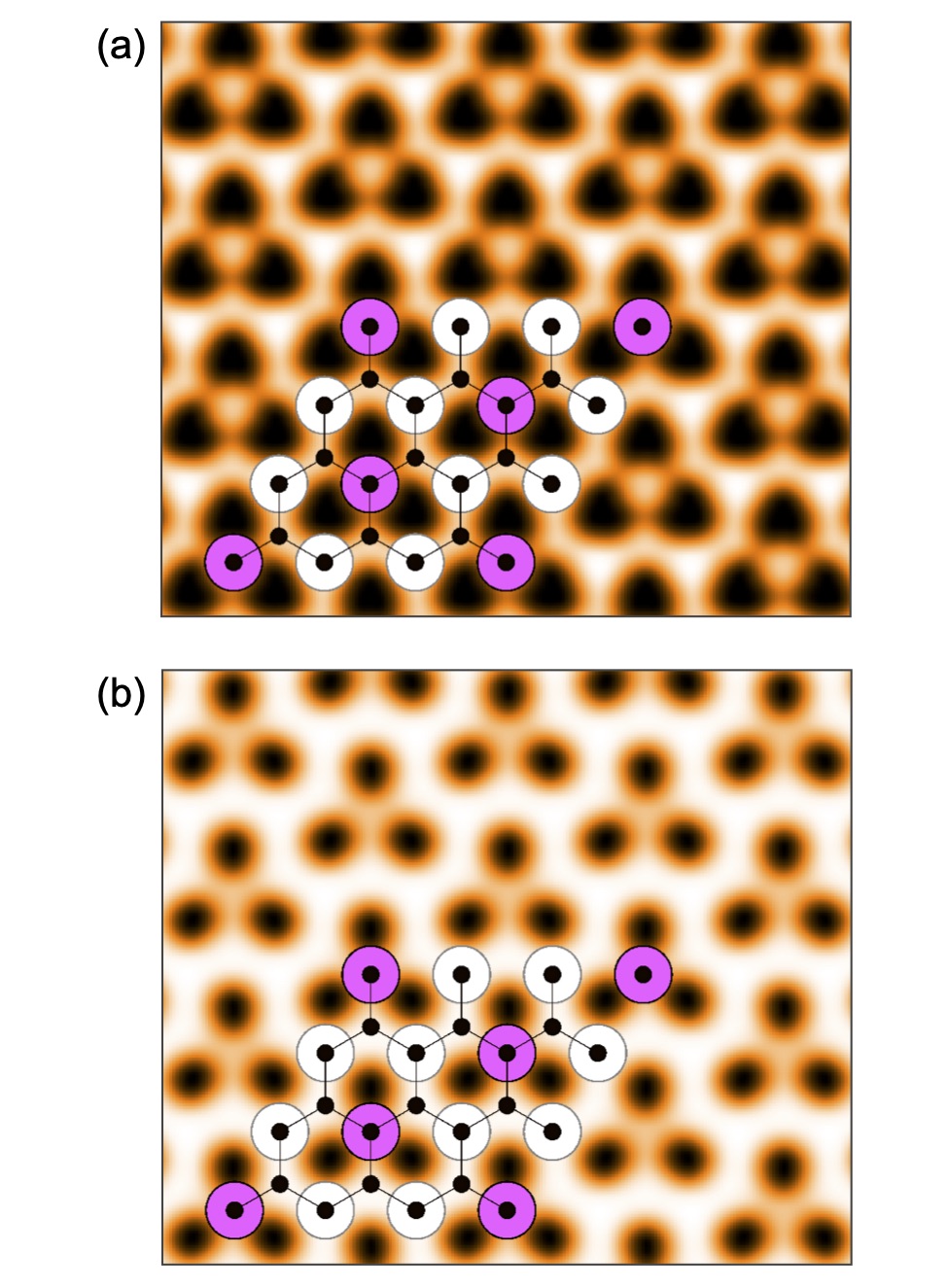
In Fig. 4 we also present calculated STM images of the graphene/Cu2Mn/ Cu(111) – model B system obtained in the framework of the Tersoff-Hamann approach for electronic states integrated between the Fermi level and energies of (a) meV and (b) meV. Both images demonstrate the appearance of the carbon rings in the STM experiment accompanied by the additional structure due to the symmetry of the Cu2Mn layer at the interface. These data can be used as a good reference in future studies of the structural and electronic properties of the graphene-Mn-Cu(111) system.
3 Conclusions
Using state-of-the-art DFT calculations the electronic properties of different systems obtained via intercalation of Mn in graphene/Cu(111) were studied. Three models were considered – sharp graphene/Mn/Cu(111) interface and two configurations for the graphene/\chCu_2Mn/Cu(111) Cu-Mn alloy-based systems. In all cases graphene is found as strongly -doped and in case of the sharp graphene/Mn/Cu(111) interface the Dirac cone is fully destroyed. For the most realistic case of the graphene-Mn-Cu(111) system, the formation of the ferromagnetic Cu2Mn alloy at the interface is found. In this case the strong magnetic moment of Mn atoms leads to the appearance of the induced magnetic moment of carbon atoms adsorbed on top of Mn. The formation of the Cu2Mn/Cu(111) slab below graphene also leads to the formation of the interesting band structure and spin topology of the graphene states in the vicinity of the point. Here, graphene-derived bands are spin split and three branches are formed around the Dirac point, which can be assigned to different carbon sublattices in a graphene layer associated with different carbon atoms adsorption sites above the Cu2Mn/Cu(111) slab. Obtained spin configuration of the graphene bands around the Fermi level could lead to different conductivity for spin-up and spin-down channels, which can be useful for the realization of the spintronics applications on the basis of graphene.
4 Experimental
Spin-polarized DFT calculations based on plane-wave basis sets of eV cutoff energy were performed with the Vienna ab initio simulation package (VASP) 46, 47, 48. The Perdew-Burke-Ernzerhof (PBE) exchange-correlation functional 49 was employed. The electron-ion interaction was described within the projector augmented wave (PAW) method 50 with C (,), Mn (,,), and Cu (,) states treated as valence states. The Brillouin-zone integration was performed on -centered symmetry reduced Monkhorst-Pack meshes using a Methfessel-Paxton smearing method of first order with eV, except for the calculation of total energies. For these calculations, the tetrahedron method with Blöchl corrections 51 was employed. The mesh for sampling the supercell Brillouin zone are chosen to be as dense as at least , when folded up to the simple graphene unit cell. Dispersion interactions were considered adding a atom-atom term as parameterized by Grimme (“D2” parameterization) 52. During structure optimization, the convergence criteria for energy was set equal to eV. The band structures calculated for the studied systems were unfolded (if necessary) to the graphene () primitive unit cell according to the procedure described in Refs. 53 and 54 with the code BandUP. The STM images are calculated using the Tersoff-Hamann formalism 55.
The studied interfaces are modeled by a slab consisting of Cu-layers, a graphene adsorbed on the top side of the slab, and a vacuum gap of at least Å. The bottom layer of the slab is protected by H-atoms. In the case of the graphene-Mn-Cu(111) system, a Mn layer is added between graphene and Cu(111). In order to describe graphene as realistically as possible, the lattice constant of copper is set to be compatible with the optimized graphene lattice constant ( Å). During the structural optimization, all the -coordinates of carbon atoms ( and -coordinates are fixed) as well as those of the top three layers of metal atoms (-coordinates) are relaxed until forces became smaller than eV/Å.
This work was supported by the National Natural Science Foundation of China (Grant No. 21973059).
The following files are available free of charge:
Additional theoretical data for the graphene-Cu(111) and graphene-Mn-Cu(111) systems.
References
- 1 Novoselov, K. S. Electric Field Effect in Atomically Thin Carbon Films. Science 2004, 306, 666–669.
- 2 Geim, A. K.; Novoselov, K. S. The Rise of Graphene. Nat. Mater. 2007, 6, 183–191.
- 3 Katsnelson, M. I.; Novoselov, K. S.; Geim, A. K. Chiral Tunnelling and the Klein Paradox in Graphene. Nat. Phys. 2006, 2 620–625.
- 4 Huard, B.; Sulpizio, J. A.; Stander, N.; Todd, K.; Yang, B.; Goldhaber-Gordon, D. Transport Measurements Across a Tunable Potential Barrier in Graphene. Phys. Rev. Lett. 2007, 98, 236803.
- 5 Novoselov, K. S.; Geim, A. K.; Morozov, S. V.; Jiang, D.; Katsnelson, M. I.;Grigorieva, I. V.; Dubonos, S. V.; Firsov, A. A. Two-Dimensional Gas of Massless Dirac Fermions in Graphene. Nature 2005, 438, 197–200.
- 6 Zhang, Y.; Tan, Y.-W.; Stormer, H. L.; Kim, P. Experimental Observation of the Quantum Hall Effect and Berry’s Phase in Graphene. Nature 2005, 438, 201–204.
- 7 Novoselov, K. S.; McCann, E.; Morozov, S. V.; Fal’ko, V. I.; Katsnelson, M. I.; Zeitler, U.; Jiang, D.; Schedin, F.; Geim, A. K. Unconventional Quantum Hall Effect and Berry’s Phase of 2 in Bilayer Graphene. Nat. Phys. 2006, 2, 177–180.
- 8 McCann, E.; Fal’ko, V. I. Landau-Level Degeneracy and Quantum Hall Effect in a Graphite Bilayer. Phys. Rev. Lett. 2006, 96, 086805.
- 9 Cao, Y.; Fatemi, V.; Fang, S.; Watanabe, K.; Taniguchi, T.; Kaxiras, E.; Jarillo-Herrero, P. Unconventional Superconductivity in Magic-Angle Graphene Superlattices. Nature 2018, 556, 43–50.
- 10 Weatherup, R. S.; D’Arsie, L.; Cabrero-Vilatela, A.; Caneva, S.; Blume, R.; Robertson, J.; Schloegl, R.; Hofmann, S. Long-Term Passivation of Strongly Interacting Metals with Single-Layer Graphene. J. Am. Chem. Soc. 2015, 137, 14358–14366.
- 11 Bae, S.; Kim, H.; Lee, Y.; Xu, X.; Park, J.-S.; Zheng, Y.; Balakrishnan, J.; Lei, T.; Kim, H. R.; Song, Y. I.; Kim, Y.-J.; Kim, K. S.; Özyilmaz, B.; Ahn, J.-H.; Hong, B. H.; Iijima, S. Roll-to-Roll Production of 30-Inch Graphene Films for Transparent Eelectrodes. Nat. Nanotechnol. 2010, 5, 574–578.
- 12 Ryu, J.; Kim, Y.; Won, D.; Kim, N.; Park, J. S.; Lee, E.-K.; Cho, D.; Cho, S.-P.; Kim, S. J.; Ryu, G. H.; Shin, H.-A.-S.; Lee, Z.; Hong, B. H.; Cho, S. Fast Synthesis of High-Performance Graphene Films by Hydrogen-Free Rapid Thermal Chemical Vapor Deposition. ACS Nano 2014, 8, 950–956.
- 13 Schedin, F.; Geim, A. K.; Morozov, S. V.; Hill, E. W.; Blake, P.; Katsnelson, M. I.; Novoselov, K. S. Detection of Individual Gas Molecules Adsorbed on Graphene. Nature Mater. 2007, 6, 652–655.
- 14 Karpan, V. M.; Giovannetti, G.; Khomyakov, P. A.; Talanana, M.; Starikov, A. A.; Zwierzycki, M.; van den Brink, J.; Brocks, G.; Kelly, P. J. Graphite and Graphene as Perfect Spin Filters. Phys. Rev. Lett. 2007, 99, 176602.
- 15 Dedkov, Y. S.; Fonin, M.; Laubschat, C. A Possible Source of Spin-Polarized Electrons: The Inert Graphene/Ni(111) System. Appl. Phys. Lett. 2008, 92, 052506.
- 16 Dlubak, B.; Martin, M.-B.; Weatherup, R. S.; Yang, H.; Deranlot, C.; Blume, R.; Schloegl, R.; Fert, A.; Anane, A.; Hofmann, S.; Seneor, P.; Robertson, J. Graphene-Passivated Nickel as an Oxidation-Resistant Electrode for Spintronics. ACS Nano 2012, 6, 10930–10934.
- 17 Dedkov, Y.; Voloshina, E. Graphene Growth and Properties on Metal Substrates. J. Phys.: Condens. Matter 2015, 27, 303002.
- 18 Yang, M.; Liu, Y.; Fan, T.; Zhang, D. Metal-Graphene Interfaces in Epitaxial and Bulk Systems: A Review. Prog. Mater. Sci. 2020, 110, 100652.
- 19 Voloshina, E.; Dedkov, Y. Graphene on Metallic Surfaces: Problems and Perspectives. Phys. Chem. Chem. Phys. 2012, 14, 13502–13514.
- 20 Pletikosic, I.; Kralj, M.; Pervan, P.; Brako, R.; Coraux, J.; N’Diaye T. A.; Busse, C.; Michely, T. Dirac Cones and Minigaps for Graphene on Ir(111). Phys. Rev. Lett. 2009, 102, 056808.
- 21 Klimovskikh, I.; Otrokov, M. M.; Voroshnin, V. Y.; Sostina, D.; Petaccia, L.; Di Santo, G.; Thakur, S.; Chulkov, E. V.; Shikin, A. M. Spin-Orbit Coupling Induced Gap in Graphene on Pt(111) with Intercalated Pb Monolayer. ACS Nano 2017, 11, 368–374.
- 22 Khomyakov, P. A.; Giovannetti, G.; Rusu, P. C.; Brocks, G.; van den Brink, J.; Kelly, P. J. First-Principles Study of the Interaction and Charge Transfer Between Graphene and Metals. Phys. Rev. B 2009, 79, 195425.
- 23 Gottardi, S.; Muller, K.; Bignardi, L.; Moreno-Lopez, J. C.; Pham, T. A.; Ivashenko, O.; Yablonskikh, M.; Barinov, A.; Bjork, J.; Rudolf, P.; Stohr, M. Comparing Graphene Growth on Cu(111) versus Oxidized Cu(111). Nano Lett. 2015, 15, 917–922.
- 24 Bertoni, G.; Calmels, L.; Altibelli, A.; Serin, V. First-Principles Calculation of the Electronic Structure and EELS Spectra at the Graphene/Ni(111) Interface. Phys. Rev. B 2005, 71, 075402.
- 25 Eom, D.; Prezzi, D.; Rim, Zhou, H.; Lefenfeld, M.; Xiao, S.; Nuckolls, C.; Hybertsen, M. S.; Heinz, T. F.; Flynn, G. W. Structure and Electronic Properties of Graphene Nanoislands on Co(0001). Nano Lett. 2009, 9, 2844.
- 26 Marchini, S.; Günther, S.; Wintterlin, J. Scanning Tunneling Microscopy of Graphene on Ru(0001). Phys. Rev. B 2007, 76, 075429.
- 27 Voloshina, E. N.; Generalov, A.; Weser, M.; Böttcher, S.; Horn, K.; Dedkov, Y. S. Structural and Electronic Properties of the Graphene/Al/Ni(111) Intercalation System. New J. Phys. 2011, 13, 113028.
- 28 Generalov, A. V.; Voloshina, E. N.; Dedkov, Y. S. Structural and Electronic Properties of Graphene-Based Junctions for Spin-Filtering: The Graphene/Al/Ni(111) Intercalation-Like System. Appl. Surf. Sci. 2013, 267, 8–11.
- 29 Voloshina, E.; Dedkov, Y. Realistic Large-Scale Modeling of Rashba and Induced Spin-Orbit Effects in Graphene/High-Z-Metal Systems. Adv. Theory Simul. 2018, 1, 1800063.
- 30 Dedkov, Y. S.; Shikin, A. M.; Adamchuk, V. K.; Molodtsov, S. L.; Laubschat, C.; Bauer, A.; Kaindl, G. Intercalation of Copper Underneath a Monolayer of Graphite on Ni(111). Phys. Rev. B 2001, 64, 035405.
- 31 Vita, H.; Böttcher, S.; Horn, K.; Voloshina, E. N.; Ovcharenko, R. E.; Kampen, T.; Thissen, A.; Dedkov, Y. S. Understanding the Origin of Band Gap Formation in Graphene on Metals: Graphene on Cu/Ir(111). Sci. Rep. 2014, 4, 5704.
- 32 Weser, M.; Voloshina, E. N.; Horn, K.; Dedkov, Y. S. Electronic Structure and Magnetic Properties of the Graphene/Fe/Ni(111) Intercalation-Like System. Phys. Chem. Chem. Phys. 2011, 13, 7534–7539.
- 33 Voloshina, E.; Guo, Q.; Paulus, B.; Böttcher, S.; Vita, H.; Horn, K.; Zhao, C.; Cui, Y.; Dedkov, Y. Electronic Structure and Magnetic Properties of Graphene/Ni3Mn/Ni(111) Trilayer. J. Phys. Chem. C 2019, 123, 4994–5002.
- 34 Profeta, G.; Calandra, M.; Mauri, F. Phonon-Mediated Superconductivity in Graphene by Lithium Deposition. Nat. Phys. 2012, 8, 131–134.
- 35 Voloshina, E.; Dedkov, Y. Graphene on Metallic Surfaces: Problems and Perspectives. Phys. Chem. Chem. Phys. 2012, 14, 13502–13514.
- 36 Tamai, A.; Meevasana, W.; King, P. D. C.; Nicholson, C. W.; de la Torre, A.; Rozbicki, E.; Baumberger, F. Spin-Orbit Splitting of the Shockley Surface State on Cu(111). Phys. Rev. B 2013, 87, 075113.
- 37 Tesch, J.; Leicht, P.; Blumenschein, F.; Gragnaniello, L.; Fonin, M.; Steinkasserer, L. E. M.; Paulus, B.; Voloshina, E.; Dedkov, Y. Structural and Electronic Properties of Graphene Nanoflakes on Au(111) and Ag(111). Sci. Rep. 2016, 6, 23439.
- 38 Tesch, J.; Voloshina, E.; Jubitz, M.; Dedkov, Y.; Fonin, M. Local Electronic Properties of the Graphene-Protected Giant Rashba-Split BiAg2 Surface. Phys. Rev. B 2017, 95, 155428.
- 39 Voloshina, E. N.; Dedkov, Y. S. General Aapproach to Understanding the Electronic Structure of Graphene on Metals. Mater. Res. Express 2014, 1, 035603.
- 40 Gao, L.; Guest, J. R.; Guisinger, N. P. Epitaxial Graphene on Cu(111). Nano Lett. 2010, 10, 3512–3516.
- 41 Schneider, J.; Rosenhahn, A.; Wandelt, K. STM Measurements on Alloy Formation During Submonolayer Growth of Mn on Cu(111). Appl. Surf. Sci. 1999, 142, 68–74.
- 42 Bihlmayer, G.; Kurz, Ph.; Blügel, S. Overlayers, Interlayers, and Surface Alloys of Mn on the Cu(111) Surface. Phys. Rev. B 2000, 62, 4726–4732.
- 43 Chen, W.; Chen, H.; Lan, H.; Cui, P.; Schulze, T. P.; Zhu, W.; Zhang, Z. Suppression of Grain Boundaries in Graphene Growth on Superstructured Mn-Cu(111) Surface. Phys. Rev. Lett. 2012, 109, 265507.
- 44 Gao, L.; Guest, J. R.; Guisinger, N. P. Epitaxial Graphene on Cu(111). Nano Lett. 2010, 10, 3512–3516.
- 45 Hofer, W. A.; Foster, A. S.; Shluger, A. L. Theories of Scanning Probe Microscopes at the Atomic Scale. Rev. Mod. Phys. 2003, 75, 1287–1331.
- 46 Kresse, G.; Furthmüller, J. Efficiency of Ab-Initio Total Energy Calculations for Metals and Semiconductors Using a Plane-Wave Basis Set. Comput. Mater. Sci. 1996, 6, 15–50.
- 47 Kresse, G.; Hafner, J. Norm-Conserving and Ultrasoft Pseudopotentials for First-Row and Transition Elements. J. Phys.: Condens. Matter 1994, 6, 8245–8257.
- 48 Kresse, G.; Hafner, J. Ab Initio Molecular Dynamics for Liquid Metals. Phys. Rev. B 1993, 47, 558–561.
- 49 Perdew, J. P.; Burke, K.; Ernzerhof, M. Generalized Gradient Approximation Made Simple. Phys. Rev. Lett. 1997, 78, 1396–1396.
- 50 Blöchl, P. E. Projector Augmented-Wave Method. Phys. Rev. B 1994, 50, 17953–17979.
- 51 Blöchl, P. E.; Jepsen, O.; Andersen, O. K. Improved Tetrahedron Method for Brillouin-Zone Integrations. Phys. Rev. B 1994, 49, 16223–16233.
- 52 Grimme, S. Semiempirical GGA-Type Density Functional Constructed With a Long-Range Dispersion Correction. J. Comput. Chem. 2006, 27, 1787–1799.
- 53 Medeiros, P. V. C.; Stafström, S.; Björk, J. Effects of Extrinsic and Intrinsic Perturbations on the Electronic Structure of Graphene: Retaining an Effective Primitive Cell Band Structure by Band Unfolding. Phys. Rev. B 2014, 89, 041407.
- 54 Medeiros, P. V. C.; Tsirkin, S. S.; Stafström, S.; Björk, J. Unfolding Spinor Wave Functions and Expectation Values of General Operators: Introducing the Unfolding-Density Operator. Phys. Rev. B 2015, 91, 041116.
- 55 Tersoff, J.; Hamann, D. R. Theory of the Scanning Tunneling Microscope. Phys. Rev. B 1985, 31, 805–813.
| System | graphene/Cu(111) | graphene/Mn/Cu(111) | graphene/Cu2Mn/Cu(111) | |
| model A | model B | |||
| 2.99 | 3.05 | |||
| 1.92 | 2.16 | |||
| 1.88 | 2.09 | |||
| — | 3.99 | 3.58 | ||
| — | 0.00 | // | ||
| — | / | |||
Supplementary materials for “Intercalation of Mn in graphene/Cu(111) interface: Insights to the electronic and magnetic properties from theory”
List of Tables and Figures:
Tab. S1: Results for the relaxed graphene/Cu(111). (in meV/u.c.) is the relative total energies per graphene unit cell (u.c.) with respect to the energetically most favourable structure. (in Å) is the distance between a graphene overlayer and the interface metal layer; (in Å) is the mean distance between the interface metal layer and the second metal layer; (in Å) is the mean distance between the second and third metal layers.
Tab. S2: Results for the relaxed graphene/Mn/Cu(111) with different magnetic configuration (FM=ferromagnetic, AFM=anti-ferromagnetic). (in meV/u.c.) is the relative total energies per graphene unit cell (u.c.) with respect to the energetically most favourable structure. (in Å) is the distance between the graphene overlayer and the interface metal layer; (in Å) is the mean distance between the interface metal layer and the second metal layer; (in Å) is the mean distance between the second and third metal layers; and (in ) is the interface/surface carbon atoms and manganese atoms spin magnetic moments.
Tab. S3: Results for the relaxed graphene/Cu2Mn/Cu(111) (model B) with different magnetic configuration (FM and AFM). Here (in meV/s.c.) is the relative total energies per graphene super cell (s.c.) with respect to the energetically most favourable structure.
Fig. S1: Top view of the crystallographic structures of graphene/Cu(111): (a) TF - the C atoms are placed directly above the Cu atoms of the first layer (top site) and the third layer (fcc site); (b) TH - the C atoms are placed directly above the Cu atoms of the first layer (top site) and the second layer (hcp site); (c) FH - the C atoms are placed directly above the Cu atoms of the third layer (fcc site) and the second layer (hcp site). The graphene units cell is marked with the blue rhombus.
Fig. S2: Top view of the crystallographic structures of graphene/Mn/Cu(111) where the Mn atoms can be located at the fcc or hcp site of Cu(111) surface, respectively while the two inequivalent carbon atoms of graphene can adopt the FH, TH or TF configuration. The graphene units cell is marked with the blue rhombus.
Fig. S3: Surface alloy model of graphene/Cu2Mn/Cu(111) system (model B) with hcp lattice, where the first layer of Cu(111) slab is replaced by \chCu2Mn surface alloy and the two inequivalent carbon atoms of graphene can adopt the FH, TH or TF configuration.
Fig. S4: Spin-resolved band structures obtained after unfolding procedure for the graphene () primitive cell for (a) graphene/Cu2Mn/Cu(111) - model A and (b) graphene/Cu2Mn/Cu(111) - model B in their energetically most favourable structures.
| Structure | Reference | |||||
|---|---|---|---|---|---|---|
| TF | Fig. List of Tables and Figures:a | |||||
| TH | Fig. List of Tables and Figures:b | |||||
| FH | Fig. List of Tables and Figures:c |
| Magnetic | Structures | Reference | ||||||||
| state | gr | Mn | ||||||||
| FM | FH | hcp | — | 2.02/1.94 | 2.14 | 2.10 | 1.62 | Fig. List of Tables and Figures:d | ||
| fcc | — | 2.02/1.94 | 2.14 | 2.10 | 1.63 | Fig. List of Tables and Figures:a | ||||
| TF | hcp | — | 1.93/1.93 | 2.13 | 2.10 | 1.68 | Fig. List of Tables and Figures:e | |||
| fcc | 2.02/1.94 | 2.13 | 2.10 | 1.62 | Fig. List of Tables and Figures:b | |||||
| TH | hcp | — | 2.02/1.94 | 2.13 | 2.11 | 1.61 | Fig. List of Tables and Figures:f | |||
| fcc | — | 1.93/1.93 | 2.12 | 2.10 | 1.70 | Fig. List of Tables and Figures:c | ||||
| AFM | FH | hcp | — | 2.04/1.98 | 2.15 | 2.10 | 0.00/0.00 | Fig. List of Tables and Figures:d | ||
| fcc | — | 2.01/1.93 | 2.10 | 2.09 | 0.00/0.00 | Fig. List of Tables and Figures:a | ||||
| TF | hcp | — | 3.22/3.22 | 2.18 | 2.11 | 0.00/0.00 | Fig. List of Tables and Figures:e | |||
| fcc | 2.04/1.98 | 2.14 | 2.10 | Fig. List of Tables and Figures:b | ||||||
| TH | hcp | — | 2.04/1.99 | 2.15 | 2.11 | 0.00/0.00 | Fig. List of Tables and Figures:f | |||
| fcc | — | 3.29/3.29 | 2.19 | 2.11 | 0.00/0.00 | Fig. List of Tables and Figures:c | ||||
| Magnetic | Reference | ||||||||
| state | |||||||||
| FH | AFM | — | 0.00 | Fig. List of Tables and Figures:a | |||||
| FM | — | 0.00 | |||||||
| TH | AFM | — | 0.00 | Fig. List of Tables and Figures:b | |||||
| FM | 0.00 | ||||||||
| TF | AFM | 0.00 | Fig. List of Tables and Figures:c | ||||||
| FM | 0.00 |
![[Uncaptioned image]](/html/2112.11845/assets/FigS1.jpg)
Fig. S1. Top view of the crystallographic structures of graphene/Cu(111): (a) TF - the C atoms are placed directly above the Cu atoms of the first layer (top site) and the third layer (fcc site); (b) TH - the C atoms are placed directly above the Cu atoms of the first layer (top site) and the second layer (hcp site); (c) FH - the C atoms are placed directly above the Cu atoms of the third layer (fcc site) and the second layer (hcp site). The graphene units cell is marked with the blue rhombus.
![[Uncaptioned image]](/html/2112.11845/assets/FigS2.jpg)
Fig. S2. Top view of the crystallographic structures of graphene/Mn/Cu(111) where the Mn atoms can be located at the fcc or hcp site of Cu(111) surface, respectively while the two inequivalent carbon atoms of graphene can adopt the FH, TH or TF configuration. The graphene units cell is marked with the blue rhombus.
![[Uncaptioned image]](/html/2112.11845/assets/FigS3.jpg)
Fig. S3. Surface alloy model of graphene/Cu2Mn/Cu(111) system (model B) with hcp lattice, where the first layer of Cu(111) slab is replaced by Cu2Mn surface alloy and the two inequivalent carbon atoms of graphene can adopt the FH, TH or TF configuration.
![[Uncaptioned image]](/html/2112.11845/assets/FigS4.jpg)
Fig. S4. Spin-resolved band structures obtained after unfolding procedure for the graphene () primitive cell for (a) graphene/Cu2Mn/Cu(111) - model A and (b) graphene/Cu2Mn/Cu(111) - model B in their energetically most favourable structures.