Anomalous ambipolar transport in depleted GaAs nanowires
Abstract
We have used a polarized microluminescence technique to investigate photocarrier charge and spin transport in n-type depleted GaAs nanowires ( cm-3 doping level). At 6K, a long-distance tail appears in the luminescence spatial profile, indicative of charge and spin transport, only limited by the length of the NW. This tail is independent on excitation power and temperature. Using a self-consistent calculation based on the drift-diffusion and Poisson equations as well as on photocarrier statistics (Van Roosbroeck model), it is found that this tail is due to photocarrier drift in an internal electric field nearly two orders of magnitude larger than electric fields predicted by the usual ambipolar model. This large electric field appears because of two effects. Firstly, for transport in the spatial fluctuations of the conduction band minimum and valence band maximum, the electron mobility is activated by the internal electric field. This implies, in a counter intuitive way, that the spatial fluctuations favor long distance transport. Secondly, the range of carrier transport is further increased because of the finite NW length, an effect which plays a key role in one-dimensional systems.
I Introduction
In the past few years, investigations of transport in semiconductor nanowires (NW’s) have gained interest because of potential applications to solar cells [1], lasers [2] and quantum computing [3]. For GaAs, it has been reported recently that GaAs NW’s grown on Si substrates have strong potentialities for charge and spin transport [4]. These NW’s are n-doped in the low cm-3 range, and are therefore on the metallic side of the Mott transition [5]. They are well-adapted for spin transport, since the donor concentration nearly corresponds with that of the maximum of the spin relaxation time [6], thus ensuring conservation of spin polarization over large distances.
It may be thought that, in such NW’s, transport of photocarriers should be difficult because of the presence of spatial fluctuations of the energy of the top of the valence band, induced by statistical spatial fluctuations of the donor concentration [7, 8]. However, it has been shown that carrier transport in this disordered system can occur over distances as large as 25 m [4]. Several phases in the spatial profiles have been observed, due to i) the buildup of internal electric fields which modify the photocarrier mobilities and ii) to the subsequent spatial redistribution of the Fermi sea for undepleted NW’s. However, no interpretation for these results has been proposed.
The present work is an experimental and theoretical analysis of charge and spin transport in NW’s grown on Si substrates. We have chosen depleted NW so that the charge spatial profiles merely reveal the buildup of the internal electric field since there is no Fermi sea. The spatial charge profile exhibits a relatively fast decrease followed by a slow tail, which weakly depends on excitation power and temperature. As found by numerical resolution of conservation equations, this tail is caused by drift transport in an internal electric field of a fraction of a V/m. These results are at variance with the predictions of the usual ambipolar model [9, 10, 11, 12, 13, 14] which predicts internal electric fields smaller by two orders of magnitude. Such large internal field is shown to build up for two reasons. Firstly, as expected for such doping level, the mobility of photoelectrons depends on the internal electric field [15]. This implies that, for charge and spin transport, metallic NW’s appear as better candidates than NW’s on the insulating side of the insulator/metal transition. Secondly, the electric field is further amplified by the finite size of the NW. It is anticipated that such large electric fields are specific to one-dimensional systems.
II Experimental
II.1 Principles
Here we study NW’s HVPE-grown on Si(111) substrates using gold-catalysis at 715 ∘C [16]. In order to reduce the surface recombination velocity, the NW’s were chemically treated by a low alkaline (pH 8.5) hydrazine sulfide solution. This produced a negligible NW etching by the solution and covered the surface by a nitride layer so that surface recombination was equivalent to that of the nearly ideal Ga1-xAlxAs/GaAs interface [17]. After passivation, the NW’s, standing on the substrate, were scraped and deposited horizontally on a grid of lattice spacing 15 m. The results presented here were obtained on a depleted NW of length 20 m and of diameter 100 nm that is smaller than the limit of 180 nm for NW depletion [4].
The NW was excited at 6K by a tightly-focused, continuous-wave, laser beam (Gaussian radius m, energy eV). Spatially-resolved spectral analysis of the intensity and circular polarization of the luminescence was performed using a setup described elsewhere [18, 4]. Using liquid crystal modulators, the sample was excited with -polarized light and the intensity of the luminescence components with helicity was selectively monitored. The luminescence intensity is the sum of these two components and given by
| (1) |
where is the photoelectron concentration, is the hole concentration and is the bimolecular recombination coefficient. Here, quite generally, we take a nonzero electron concentration in the dark . This value will be zero for the experimental depleted NW’s but will have a weak nonzero value for computations. The difference signal is equal to , where for - polarized excitation. Here , where are the concentrations of electrons with spin , choosing the excitation light direction as the quantization axis, is the spin density.
II.2 Results
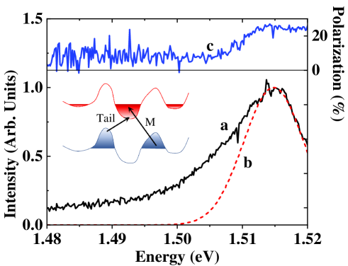
The nearbandgap luminescence and polarization spectra, taken at the excitation spot, are shown in Fig. 1. The lattice temperature is 6K and a very small excitation power of W is chosen. More details are shown in the supplementary material. The luminescence spectrum peaks near the bandgap energy. It can be decomposed into a main line, approximated by a gaussian lineshape of half-width 6.5 meV (curve b), and a low-energy tail which extends down to 1.48 eV. As shown in the inset of Fig. 1, this tail is attributed to spatially indirect transitions, where the transition energy is lowered by local electric fields in the fluctuations.
Curve c of Fig. 1 shows the corresponding polarization spectrum. For energies larger than 1.51 eV, the polarization has a very large value above 20 , implying a photoelectron spin polarization close to the maximum value of . This suggests a very large spin relaxation time, as predicted for this sample where the Bir-Aronov-Pikus (BAP) process is weak because of the weak hole concentration [19, 6]. Note that the polarization increases near 1.504 eV, which coincides with the onset of the gaussian component of the intensity spectrum. This is because the electron quasi Fermi level lies above the minimum of the conduction band fluctuations so that electrons below this level are degenerate.
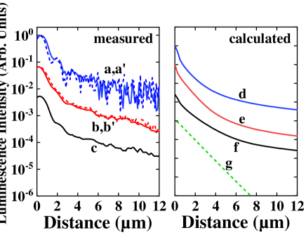
Shown in curve a of Fig. 2 is the intensity spatial profile, taken in the same conditions as curve a of Fig. 1. Curve a’ shows the profile of the difference signal . The two spatial profiles are quite similar. This shows that the photoelectron spin polarization is constant over the profile. This is expected in our case where the spin relaxation time is large, as suggested by the large photoelectron spin polarization. The spatial profile is composed of a rapid decrease up to 2 m, with a slower decrease for larger distances, superimposed on fluctuations which are reproducible from one curve to the other. These fluctuations may be caused by inhomogeneities of the surface recombination or by uncomplete spatial averaging of the microscopic potential fluctuations described in the inset of Fig. 1.
Such shape is very different from a single exponential, which is the predicted profile for one dimensional unipolar transport (see supplementary information of Ref. [4]). The observation of the long distance tail implies that, although most carriers recombine near the place of excitation, a significant fraction escape from the potential fluctuations at the place of excitation and can be transported over large distances. Since hopping processes are easier for electrons than for holes because of their weaker effective mass, there builds up an outwards internal electric field which in turn drives photoholes out of the excitation spot provided its magnitude is comparable to that of the electric field of the fluctuations (of the order of the unscreened effective field near a donor m, where is the donor binding energy and is the effective Bohr radius).
Shown in curves b and b’ of Fig. 2 are the intensity and difference spatial profiles obtained for a larger excitation power of 1 mW. In the same way as for a smaller excitation power, the two curves are similar, revealing that the photoelectron spin polarization does not decrease during transport. Comparison between Curves a and b reveals that, unlike observed earlier for ambipolar transport in 3D samples [9, 10, 11, 12, 13, 14], the excitation power has little effect on the spatial profiles.
Curve c was taken in the same conditions as Curve b but at a higher lattice temperature of 30K, leading to a decrease of luminescence intensity by about one order of magnitude. This curve is quite similar to Curve a and Curve b, implying that temperature has a weak effect on the spatial profile. Such result may appear surprising, in view of the strong temperature dependence of the conductivity reported for metallic systems [5].
III Interpretation
The results of the preceding section show that depleted NW’s on the metallic side of the insulator/metal transition appear as ideal candidates for charge and spin transport. Transport exhibits a long distance tail up to 15 m, mostly limited by the NW end. The photoelectron polarization at the excitation spot is close to its maximum value determined by the transition probabilities and weakly decreases during transport.
In order to interpret these results, calculation of the spatial distributions of electrons and holes was performed using the Van Roosbroeck model [20]. For holes, the drift-diffusion equation is
| (2) |
Here is the rate of creation of electron-hole pairs, is the absolute value of the electron charge, is the hole nonradiative recombination time and is the hole current. The corresponding spin-unresolved equation for electrons is
| (3) |
where is the electron nonradiative recombination time. The quadratic dependence of the spatially-integrated luminescence intensity on excitation power (see Supplementary Material) shows that nonradiative recombination is dominant over radiative recombination. Since the two recombination terms must be equal after spatial integration which removes the effect of transport, and within the hypothesis of charge neutrality (i. e. that the total photoelectron and photohole charges are equal) one can assume that . The electron and hole currrents are given by
| (4) |
and
| (5) |
where are the electron (hole) mobilities and are the corresponding diffusion constants. Here ( ) is the energy of the electron (hole) Fermi level with respect to its value at equilibrium. The electronic concentration can be expressed by Boltzmann statistics
| (6) |
where is Boltzmann’s constant, is the photocarrier temperature and is the energy of the bottom of the conduction band. As discussed in the supplementary material, the hole energy distribution for a depleted NW is closer to a Boltzmann one than for an undepleted one. This distribution will be approximated by
| (7) |
where is the energy of the top of the valence band. Here () is the effective density of states of the conduction (valence) band, and is the energy of the bottom of the conduction band. Here is the spatially-dependent potential, given by Poisson’s equation, which can be written, for a spatially homogeneous doping
| (8) |
where is the static permittivity.
For NW’s on the metallic side of the insulator/metal transition, transport occurs through hopping processes assisted by the electric field. This results in a dependence of the mobility on the electric field [15, 21, 22], given by
| (9) |
where is the mobility at large electric fields. The electric field is given by
| (10) |
where is a characteristic energy, is the length of an elementary hopping process, and . Here, one will use the approximate expression in Eq. 9 since, as shown by the weak effect of temperature on the profile, one probably has . One may think that the hole mobility also depends on electric field. However, such dependence has no effect on the spatial profiles, since hole diffusive and drift currents are negligible with respect to their electronic counterparts and will not be included here [23].
The coupled equations 2, 3 , 6, 7 and 8 must be solved self-consistently. The calculations give the spatial distribution of , and and subsequently the spatial profiles of , and . Finally, the spatial profile of the luminescence intensity is given by Eq. 1.
Independently, the expression of the internal electric field is obtained by comparing Eq. 2 and Eq. 3. This gives
| (11) |
where and , given by Eq. 4 and Eq. 5, respectively, depend on electric field via the contribution of drift currents. Within what will be called below the usual ambipolar model, one assumes a spatially-infinite sample with negligible charge concentrations and electric field at its end [9, 10, 11]. One also assumes charge neutrality (). Thus, the sum of electron and hole currents which is zero at infinity, is also zero at all points in the NW, so that
| (12) |
Although, as seen in Sec. IV below, Eq. 12 must be modified to correctly interpret the long distance tail, it allows us to understand the weak dependence of the luminescence intensity profiles on excitation power. Indeed, provided , multiplication of electron and hole concentrations by a common factor will not affect the electric field and therefore the shape of the spatial profile. The weak dependence of the spatial profile on temperature is in agreement with the observed weak temperature dependence of the photoconductivity of disordered systems [15, 21]. Such effect can be understood if, in Eq. 9, . In this case, the electron mobility nonlinearly depends on electric field according to the approximate Eq. 9 and weakly depends on temperature.
For solving the above coupled equations, we applied a Newton-Raphson algorithm, as described in Ref. [24], to a NW of length m with an excitation spot at m from the end. For the boundary conditions, one imposed a zero potential at the NW ends and a zero recombination current at the lateral surfaces. In order to avoid divergence, a nonzero value of and a zero value of were used as a starting point for the calculations. The quantity was subsequently decreased to cm-3 and was progressively increased to above V/m. The high-field mobility values were cm and cm that is, slightly larger than mobilities for a degenerate doping level [25]. This is probably because the absence of intrinsic electrons increases the electron and hole collision time. The values of the other parameters were found to have a negligible effect on the profile. The electron and hole lifetimes were ns. The temperature was taken to 30 K.
We first consider the case of a doping level slightly smaller than the insulator/metal transition. Since the spatial fluctuations of the conduction band minimum and valence band maximum are negligible [26], one can take . The calculated luminescence spatial profile is shown in Curve g of Fig. 2. The excitation power was W i. e. close to that used in Curve a. The profile exhibits a rapid, approximately exponential, decrease, nearly independent on excitation power and does not interpret the experimental results. At the excitation spot, the electric field is zero for symmetry reasons. Away from the excitation spot, the electric field is estimated using Eq. 12, to where is the exponential slope of the decrease. Using m and the Einstein relation , where is an energy of the order of the band fluctuation amplitude [15] and assuming charge neutrality, we obtain V/m. This relatively weak value implies that diffusive currents are larger than drift currents and explains the absence of a long-distance tail. It is concluded that NW’s of a doping level on the insulating side of the Mott transition are not expected to be good candidates for charge and spin transport.
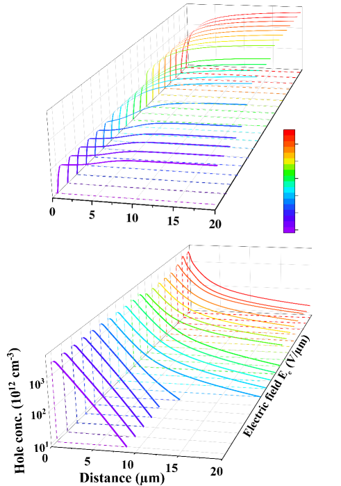
For increasing values of , the calculated photohole concentration profiles for an excitation power of 150 W are shown in Panel A of Fig. 3. Panel B shows the corresponding spatial profiles of the electric field. In agreement with the experimental results, and provided V/m, the calculated concentration profiles exhibit a long distance tail at a distance larger than m . In this regime, the profile weakly depends on . An estimate of can be obtained, using Eq. 10 taking meV, corresponding to the amplitude of the fluctuations [26] and . One finds V/m. This is a high estimate of since the electron hopping process may occur over larger distances. However, is in all cases larger than V/m so that a long distance tail should appear.
The internal electric field at a distance from the excitation spot larger than m is of several V/m i. e. nearly two orders of magnitude larger than for the ambipolar case. This suggests that the tail in the hole concentration profile is caused by outward hole and electron drift in the electric field.
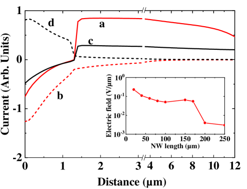
In order to confirm this hypothesis, we have calculated the spatial profiles of the electron and hole currents, using V/m. As seen in Fig. 4, two spatial phases are visible. Up to a distance of m, because of the large concentration gradient, diffusive currents are larger than drift currents. For larger distances, drift currents indeed predominate, because of the large electric field. These currents explain the presence of charge and spin transport over record distances. Note that the electron drift (Curve a) and diffusive (Curve b) currents are, as expected, dominant over their hole counterparts (Curves c and d respectively). This justifies the hypothesis taken above of a negligible field dependence of the hole mobility [23].
Curve d of Fig. 2 shows the calculated intensity spatial profile, taking for specificity V/m. This profile is similar to the experimental one, shown in Curve a. Curve e of Fig. 2 shows the calculated spatial intensity profile for an effective increased excitation power of 1 mW. Again, this curve is similar to both the experimental Curve b, taken for an equivalent excitation power, and Curve d, implying that the calculated profile weakly depends on excitation power. Finally, Curve f shows the intensity profile calculated using . This curve is similar to Curve e showing, in agreement with the experimental results and with Eq. 10, that the temperature increase has little effect on the profile.
IV Origin of the large value of the internal electric field
It is firs shown that the tail in the luminescence spatial profile cannot be explained by the usual ambipolar model [Eq. 12], even if a field-activated electron mobility is included. In order to evaluate the electric field in this case, one uses , as found from Eq. 3 assuming that drift currents are larger than diffusive currents. Further using Einstein’s relation, one obtains
| (13) |
The electric field , given by , is V/m, with the parameter values used in Sec. III, and taking . Numerical resolution of this equation shows that the fraction in the right hand is close to unity and can be approximated as shown in Eq. 13. Up to V/m, Eq. 13 has a solution close to . This value is comparable with usual ambipolar fields. It does not interpret the results and is in contradiction with the starting hypothesis of large drift currents.
This failure is not caused by a possible breaking of the hypothesis of charge neutrality, since numerical simulations confirm its validity for calculating the electric field [27], except in a short stretch near the NW end. We propose that the reason why Eq. 13 cannot explain the large electric field is that, because of the slow tail, the photocarrier concentrations and currents near the NW end cannot be neglected. Integration of Eq. 11 between coordinates and shows that it is necessary to replace Eq. 12 by
| (14) |
where is the sum of drift currents at position in the slow tail. Here, is chosen to be sufficiently large so that, as shown in Fig. 4, the diffusive current at is negligible. Inclusion of the negative term in Eq. 14 should result in an increase of the electric field. In order to verify this hypothesis, we have calculated the spatial profiles for increasingly large values of the NW length. The inset of Fig. 4 shows the electric field values at a distance of 10 m from the excitation spot. Up to a NW length of 170 m, the electric field weakly depends on distance and is of V/m. For a further increase of NW length, one observes a strong decrease of electric field down to V/m that is, to a value comparable with the usual ambipolar regime. It is concluded that, at least for the parameter values chosen here, the anomalous ambipolar transport is amplified by NW finite size effects, provided the NW length is smaller than 170 m. This length is smaller than the maximum length of usual NW’s.
The inset of Fig. 4 shows that the transition between the two regimes occurs over a narrow range of 30 m of NW length, while the electric field is nearly constant before and after the transition. In the same way, Fig. 3 shows that the transition as a function of occurs over only a factor of 3 of variation of with profiles nearly independent on before and after the transition. These features reveal that the transition between the two regimes occurs through a critical process. This can be understood qualitatively, assuming that and that the photocarrier concentrations at are fractions of their values at position [ and ]. The approximate equation Eq. 13 is still valid, provided is divided by . This induces an increase of and therefore of the electric field. This will in turn induce an increase of since this quantity also depends on electric field, according to ]. The quantity is then closer to unity, which will induce a further increase of electric field.
V Conclusion
it is shown that depleted NW’s on the metallic side of the insulator/metal transition (low cm-3 range) appear as ideal candidates for charge and spin transport : i) The spatial profiles of the luminescence intensity exhibit a long distance tail, weakly dependent on excitation power and temperature, concerning about of the photocarriers and characterized by a decay length larger than 15 m. ii) The spin polarization also weakly decreases with distance.
A self-consistent coupled resolution of the drift-diffusion equations, using the Poisson equation and Boltzmann statistics (Van Roosbroeck model) shows that the tail occurs because of photocarrier drifting in an internal electric field as large as m. Two ingredients are crucial for building up such a large electric field : i) the dependence of the photoelectron mobility on internal electric field which strongly increases the elecron mobility and results in a field-assisted transport. ii) Critical amplification of these effects caused by the NW finite size..
Note finally that the above reasoning are only valid for one dimensional systems i. e. if the lateral dimension is smaller than the typical decay length. Indeed, calculations on 2D systems, with increasing , have not revealed any transition to a slow tail. Since only a limited number of parameter values was chosen, these results need to be confirmed by further experimental and theoretical investigations, which are out of the scope of the present work. However, this suggests that the one dimensional nature of the NW’s plays a key role and that NW’s are better candidates for charge and spin transport than 2D or 3D systems.
Acknowledgements.
We are grateful to V. L. Berkovits and to P. A. Alekseev for advices in the chemical surface passivation. This work was supported by Région Auvergne Rhône- Alpes (Pack ambition recherche; Convention 17 011236 01- 61617, CPERMMASYF and LabExIMobS3 (ANR-10- LABX-16-01). It was also funded by the program Investissements d ’avenir of the French ANR agency, by the French governement IDEX-SITE initiative 16-IDEX-0001 (CAP20- 25), the European Commission (Auvergne FEDER Funds).References
- Krogstrup et al. [2013] P. Krogstrup, H. I. Jorgensen, M. Heiss, O. Demichel, J. V. Holm, M. Aagesen, J. Nygard, and A. F. y Morral, Nature Photonics 7, 306 (2013).
- Duan [2003] X. Duan, Nature 421, 241 (2003).
- VandenBerg [2013] J.W.G. vandenBerg, S. Nadj-Perge, V.S. Pribiag, S.R. Plissard, E.P.A.M. Bakkers, S.M. Frolov, L.P. Kouwenhoven, Phys. Rev. Lett. 110, 066806 (2013).
- Hijazi et al. [2021] H. Hijazi, D. Paget, G. Monier, G. Grégoire, J. Leymarie, E. Gil, F. Cadiz, C. Robert-Goumet, and Y. André, Phys. Rev B 103, 195314 (2021).
- Benzaquen et al. [1987] M. Benzaquen, D. Walsh, and K. Mazuruk, Phys. Rev. B 36, 4748 (1987).
- Dzhioev et al. [2002] R. I. Dzhioev, K. V. Kavokin, V. L. Korenev, M. V. Lazarev, B. Y. Meltser, M. N. Stepanova, B. P. Zakharchenya, D. Gammon, and D. S. Katzer, Phys. Rev. B 66, 245204 (2002).
- Efros et al. [1972] A. L. Efros, Y. S. Halpern, and B. I. Shklovsky, Proceedings of the International Conference on Physics of semiconductors, Warsaw 1972 (Polish Scientific publishers, Warsaw, 1972).
- Shklovskii and Efros [1984] B. I. Shklovskii and A. L. Efros, Electronic Properties of Doped Semiconductors (Springer-Verlag, Berlin, 1984).
- Smith [1978] R. A. Smith, Semiconductors (Cambridge University Press, Cambridge, 1978).
- Zhao et al. [2009] H. Zhao, M. Mower, and G. Vignale, Phys Rev. B 79, 115321 (2009).
- Cadiz et al. [2015a] F. Cadiz, D. Paget, A. C. H. Rowe, L. Martinelli, and S. Arscott, Appl. Phys. Lett 107, 092108 (2015a).
- Cadiz et al. [2015b] F. Cadiz, D. Paget, A. C. H. Rowe, and S. Arscott, Phys. Rev. B 92, 121203(R) (2015b).
- Cadiz et al. [2017] F. Cadiz, D. Lagarde, P. Renucci, D. Paget, T. Amand, H. Carrere, A. C. H. Rowe, and S. Arscott, Appl. Phys. Lett. 110, 082101 (2017).
- Paget et al. [2012] D. Paget, F. Cadiz, A. C. H. Rowe, F. Moreau, S. Arscott, and E. Peytavit, Journal of Applied Physics 111, 123720 (2012).
- Baranovskii and Rubei [2017] S. Baranovskii and O. Rubei, Charge Transport in Disordered Materials (Springer Handbook of Electronic and Photonic Materials, Ed. S. Kasap and P. Capper, Ch. 9, Springer-Verlag, Berlin, 2017).
- Hijazi et al. [2018] H. Hijazi, V. G. Dubrovskii, G. Monier, E. Gil, C. Leroux, G. Avit, A. Trassoudaine, C. Bougerol, D. Castellucci, C. Robert-Goumet, et al., J. Phys. Chem C 122, 19230 (2018).
- Alekseev et al. [2015] P. A. Alekseev, M. S. Dunaevskiy, V. P. Ulin, T. V. Lvova, D. O. Filatov, A. V. Nezhdanov, A. I. Mashin, and V. L. Berkovits, Nanolett 15, 63 (2015).
- Favorskiy et al. [2010] I. Favorskiy, D. Vu, E. Peytavit, S. Arscott, D. Paget, and A. C. H. Rowe, Rev. Sci. Instr. 81, 103902 (2010).
- Bir et al. [1975] G. L. Bir, A. G. Aronov, and G. E. Pikus, JETP 42, 705 (1975).
- van Roosbroeck [1953] W. van Roosbroeck, Phys. Rev. 91, 282 (1953).
- Cleve et al. [1995] B. Cleve, B. Hartenstein, S. D. Baranovskii, M. Scheidler, P. Thomas, and H. Baessler, Phys. Rev B 51, 16705 (1995).
- Hijazi et al. [2020] H. Hijazi, D. Paget, G. Monier, G. Grégoire, J. Leymarie, E. Gil, F. Cadiz, C. Robert-Goumet, and Y. André, http://arxiv.org/abs/2012.08421 (2020).
- not [a] Such result has been verified by introducing a field dependence of the hole mobility, according to where is the high-field value of the hole mobility, and by performing a numerical calculation of the profile for increasing values of .
- Farrell et al. [2016] P. Farrell, N. Rotundo, D. H. Doan, M. Kantner, J. Fuhrmann, and T. Koprucki, Numerical methods for drift diffusion models (Weierstrasz Institut, Berlin, 2016).
- Lovejoy et al. [1995] M. L. Lovejoy, M. R. Melloch, and M. S. Lundstrom, Appl. Phys. Lett 67, 1101 (1995).
- Lowney [1986] J. R. Lowney, Journ. Appl. Phys. 60, 2854 (1986).
- not [b] Using Poisson’s equation and taking m, decreasing with a characteristic distance of mwe estimate cm-3 that is, 4 orders of magnitude smaller than the carrier concentration at the excitation spot.