Observation and manipulation of a phase separated state in a charge density wave material
Abstract
The 1T polytype of \chTaS2 has been studied extensively as a strongly correlated system. As 1T-\chTaS2 is thinned towards the 2D limit, its phase diagram shows significant deviations from that of the bulk material. Optoelectronic maps of ultrathin 1T-\chTaS2 have indicated the presence of non-equilibrium charge density wave phases within the hysteresis region of the nearly commensurate (NC) to commensurate (C) transition. We perform scanning tunneling microscopy on exfoliated ultrathin flakes of 1T-\chTaS2 within the NC-C hysteresis window, finding evidence that the observed non-equilibrium phases consist of intertwined, irregularly shaped NC-like and C-like domains. After applying lateral electrical signals to the sample we image changes in the geometric arrangement of the different regions. We use a phase separation model to explore the relationship between electronic inhomogeneity present in ultrathin 1T-\chTaS2 and its bulk resistivity. These results demonstrate the role of phase competition morphologies in determining the properties of 2D materials.
Strongly correlated electronic systems exhibit rich phase diagrams often characterized by competing phases with different kinds of order.Dagotto (2005) Charge, spin, lattice, and orbital degrees of freedom can all contribute to the existence of a variety of states exhibiting a range of bulk properties, including high-temperature superconductivity and electronic inhomogeneity.Battisti et al. (2017); Sun et al. (2021); Fradkin et al. (2015) Furthermore, in these complex systems, novel, emergent behaviors are observed that depend on both the properties of the phases involved and the nature of the competition between them. Depending on the balance of competition between the different states, small external stimuli have the potential to result in large changes in bulk observables,Uehara et al. (1999) a behavior that could be harnessed for sensing or memory devices.
The transition metal dichalcogenide (TMD) 1T-\chTaS2 is a van der Waals material that displays many of the features associated with complex systems. 1T-\chTaS2 exhibits strong electron correlations, is a Mott insulator at low temperatures, and has a rich phase diagram comprising a variety of charge density wave (CDW) phases.Wilson et al. (1975) The material undergoes a series of successive first-order phase transitions upon cooling: starting as a normal metal, it forms an incommensurate CDW (IC) at , a nearly commensurate CDW (NC) at , and lastly a commensurate CDW (C) at . Each of these phases has a characteristic electronic, structural and orbital order,Ritschel et al. (2015) and a jump in resistivity is observed with each transition as the material becomes more insulating as it is cooled.
Moving beyond the equilibrium phases of 1T-\chTaS2, the phase diagram is expanded through the application of certain external stimuli,Sipos et al. (2008); Ma et al. (2016); Cho et al. (2016); Stojchevska et al. (2014); Vaskivskyi et al. (2016) by modifying select material parameters,Yu et al. (2015) or by thinning the material to the ultrathin limit ( thick). Previous results in ultrathin flakes of 1T-\chTaS2 have indicated that within the hysteresis region of the NC-C transition, the resistivity of the material can be bidirectionally switched, driven reversibly through intermediate states whose resistivities lie between the extrema values associated with the NC and C states.Patel et al. (2020); Hollander et al. (2015); Yoshida et al. (2015); Ma et al. (2019) While this property suggests the use of this material as a memory element in future technologies, the nanoscopic nature of these non-equilibrium intermediate phases remains an open question. Efforts to characterize the CDW phases in 1T-\chTaS2 have typically focussed on bulk samples, within regions of the phase diagram where the CDW states are well-defined. Only recently have attempts been made to specifically study the spatial characteristics of the phases present in flakes within the NC-C hysteresis region, but these experiments have been limited to characterizing the phases at the micron length scale.Patel et al. (2020); Ludwiczak et al. (2020); Frenzel et al. (2018)
In this work, the nanoscopic nature of the CDW states in the hysteresis region of the NC-C phase transition of ultrathin 1T-\chTaS2 is elucidated. We image exfoliated flakes using scanning tunneling microscopy (STM) and observe the existence of an inhomogeneous electronic state. Additionally, we image changes in this state after the application of lateral electrical signals and after repeated rastering of the STM tip. The ability to tune the resistivity of the material within the NC-C phase transition region is revisited, and many of the observed features are re-examined within the context of the initial state being a phase separated state. Key characteristics of the intermediate states accessed within the NC-C phase transition are captured by a phase separation model based on time-dependent Ginzburg-Landau theory.
1T-\chTaS2 is known to oxidize in ambient conditionsTsen et al. (2015) and thus previous STM experiments on bulk 1T-\chTaS2 have typically relied upon in situ cleaving of crystals to expose a clean surface.Wu and Lieber (1989); Thomson et al. (1994); Burk et al. (1991); Wu and Lieber (1990) In this work, the exfoliated ultrathin samples measured were fabricated using a polymer transfer technique under an inert atmosphere, and were only exposed to air prior to being loaded into the STM (). While residues remained from processing the device, clean regions of interest were located and imaged by first mapping out a navigational path that avoided existing surface contamination. The STM was equipped with four electrical contacts, allowing for the resistance of the sample to be measured and for lateral electrical signals to be applied to the device.
Figure 1c illustrates the design of the samples.
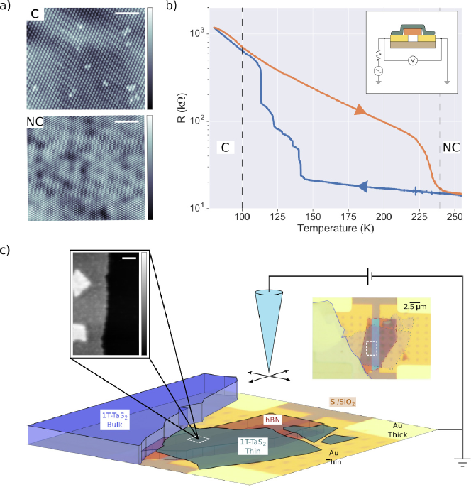
Gold contacts separated by a wide gap are lithographically defined on a \chSiO2/\chSi substrate. Hexagonal boron nitride (\chhBN) is transferred first, spanning the gap, followed by an ultrathin flake of 1T-\chTaS2 that makes contact with the gold pads on either side of the \chhBN. The \chhBN provides a substrate that is more electronically clean and atomically flat compared to the \chSiO2 surface. Markers written on the gold contact pads using electron beam lithography allow for navigation to regions of interest (Figure 1c). Initial contact in the vicinity of the flake is facilitated by patterning gold regions with different thicknesses such that the contrast is visible through a telescope attached to an optical port of the STM. With this device design it is possible to correlate changes in electronic structure with changes in the bulk electrical properties of the exfoliated flakes being measured.
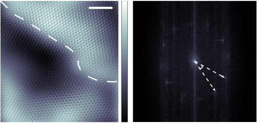
The data presented in Figure 2 and Figure 3 was collected from an approximately thick flake with lateral dimensions of . The sample was cooled from to , within the NC-C transition hysteresis region, and was imaged where the flake lies on the gold contact pad and also within the conductance channel where the flake lies on \chhBN. A filtered, topographic image of the flake on the gold contact pad is given in Figure 2a.
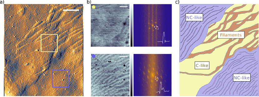
On both the contact pad and the \chhBN, the topography exhibits spatial inhomogeneity with two distinct region types, distinguishable by the presence or absence of bright striations. These striations are reminiscent of the domain walls present in the bulk NC phase of 1T-\chTaS2,Wu and Lieber (1989); Thomson et al. (1994) and thus, throughout this work, we use the label "NC-like" to identify the regions where striations are observed, and "C-like" to identify the other region type. Fast Fourier transforms (FFTs) of each region type (Figure 2b) support this identification. The FFTs of the NC-like regions contain satellite peaks in addition to the fundamental CDW modes. The existence of satellite peaks is indicative of the presence of domains.Thomson et al. (1994) In the FFT of the C-like region only the fundamental, three-fold symmetric CDW modes are observed. It is important to note that the observed state is not simply an NC state with asymmetrically arranged domain walls nor is it an NC state with a domain wall period different from the equilibrium NC value as has been previously suggested,Patel et al. (2020); Ma et al. (2019) but rather the state is specifically composed of defined, irregularly shaped NC-like and C-like domains.
The domain walls in the NC-like region in Figure 2c lack three-fold symmetry and are instead similar to the discommensurations observed in the bulk T phase.Tanda et al. (1984); Tanda and Sambongi (1985) Ginzburg-Landau theory is often used for describing a triple CDW material, like 1T-\chTaS2, with wave vectors , .McMillan (1976); Nakanishi et al. (1977) All of the bulk phases of 1T-\chTaS2 are known to satisfy the triple-Q condition, . While the wave vectors of the C, NC and IC phases are oriented degrees apart, in the T phase this constraint is relaxed.Nakatsugawa et al. (2020) The fundamental CDW wave vectors in the NC-like region found in Figure 2c have the same characterization as the T phase, in that they satisfy the triple-Q condition while the angles between the wave vectors are not equal to .
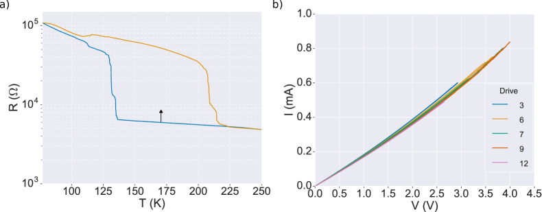
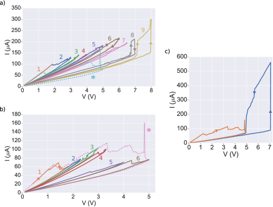
To perform bidirectional resistance switching, we initially start in the low resistance state at , and run a series of linear sweeps of laterally applied voltage, increasing the maximum voltage set with each sweep (Figure SI 7a). Figure 3a illustrates one set of STM images taken before and after a set of electrical signals were applied. In this particular case, the sweep rate was and the maximum voltage was . After the voltage sweeps, the measured resistance had increased by only (Figure SI 6b).
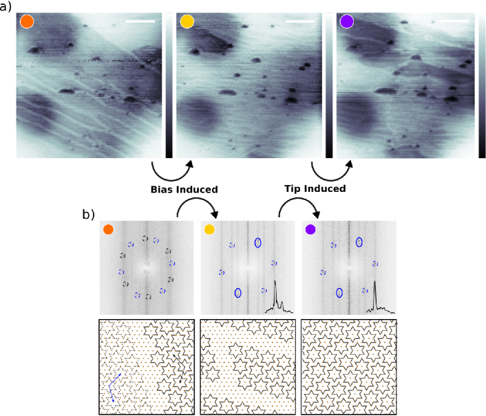
Similar to Figure 2a, distinct NC-like and C-like regions are observed prior to applying a bias across the sample. After electrically driving the flake, the NC region now dominates the image. Considering the minimal change in the bulk resistance of the material, in this instance the driving acted to rearrange the domains of the initial microstructure.
In addition to the changes caused by the application of an electric field, we also observe interconversion between the domain types as a consequence of the rastering STM tip. The rightmost scan in Figure 3a was taken following the electrical driving and illustrates the effect of the tip on the inhomogeneous state. With repeated scanning of the tip, at a tunneling voltage of , NC-like regions of the sample within the scanning area were converted to C-like regions. Unlike what is observed during the electrical driving, the overall resistance of the sample did not change from one scan to the next, indicating that the differences in the scans were due to the local perturbation of the tip rather than being a part of a global thermodynamic process.
The full evolution of the state can be clearly seen in the changes in the FFTs of consecutive STM scans (Figure 3b). Initially, the FFT contains 12 peaks. There are two possible chiral orientations of the CDW that arise in 1T-\chTaS2, often referred to in the literature as the and orientations.Zong et al. (2018) The initial STM scan in Figure 3a contains a mirror domain wall separating an NC-like region of the CDW in the orientation from a C-like region of the CDW in the orientation. Consequently, both chiral modes are observed in the FFT of the image, resulting in the appearance of 12 peaks (Figure SI 5). After lateral electrical driving of the sample, the NC region dominates the image and thus the FFT now only contains 6 peaks, representing a single orientation of the CDW. Consistent with the prevalence of the NC-like region in the image, a satellite peak in the FFT is visible. As the area is subsequently scanned, the NC region is gradually converted into the C phase, and thus in the FFT of the final scan the satellite peak is no longer present.
Given the temperature at which the STM measurements were performed, and the similarities between the features observed and the known structure of the phases present in bulk 1T-\chTaS2, we believe the data indicates that the ultrathin flake is in a phase separated state. Hysteresis in an observable through a first-order phase transition is typically indicative of the presence of superheating/supercooling.Chaikin and Lubensky Within the hysteresis region, the two phases involved in the transition are nearly degenerate and can coexist, forming a phase separated state characterized by a complex microstructure consisting of intertwined domains of the ground state of the system and the nearly degenerate metastable state. The data presented in Figure 2 and Figure 3 provides evidence for the presence of phase separation in ultrathin 1T-\chTaS2, with the electronic state imaged comprising irregularly shaped domains of C-like and NC-like regions of a size on the order of hundreds of nanometers.
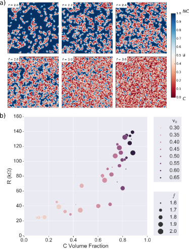
Additional evidence for the presence of phase separation in ultrathin 1T-\chTaS2 can be found in the thickness dependent resistivity of the material over the same temperature range. In bulk flakes, measurements of the resistivity through the NC-C transition are hysteretic. As 1T-\chTaS2 is thinned, the hysteresis region exhibits marked changes. In the ultrathin regime stepwise transitions are observed (Figure 1b), and as the D limit is approached, the region widens until at a thickness of ( atomic layers), the jump in the resistivity disappears altogether.Tsen et al. (2015) This result is potentially consistent with a disorder-induced phase separated state,Dagotto et al. (2001) and suggests that ultrathin flakes of 1T-\chTaS2 cooled below the NC-C transition temperature are prone to spatial inhomogeneity.
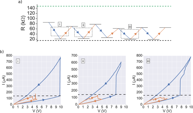
The data collected in this work does not preclude the possibility that the driving of the inhomogeneous electronic state involves a continuous evolution towards the C phase, such as through a modification of the domain period in NC-like regions with the creation or annihilation of domain walls. However, many of the features observed in the bidirectional resistance switching of ultrathin 1T-\chTaS2 can be explained by the system being in a phase separated state. For a flake in a phase separated state, the bulk resistivity is determined by the arrangement and relative volume fractions of the NC-like and C-like domains, with the initial volume fractions being set by the temperature of the system. Given the nonuniformity of the charge ordering in a phase separated state, an applied voltage drops asymmetrically across the sample. When the flake is in the low resistance state, there exists a percolative NC path, and the voltage drops across the NC region spanning the sample. The applied electric field stabilizes the C phase relative to the NC phase, causing the C state volume fraction to increase until the percolative NC path no longer exists and the resistance increases. With an increase in the C phase volume fraction, less of the applied voltage drops across NC domains, causing the driving to halt at an intermediate resistance value (Figure 4a). As the voltage is increased further, current flow through the C domains increases until breakdown occurs and the metallic percolative path is again formed, causing the resistance to decrease. With the breakdown of the C domains, the voltage again drops across an NC path, and consequently it is possible to observe a transition back into a more resistive state (Figure SI 7c). This result was previously seen in the literature where the authors were unable to drive the sample back to the low resistance value.Patel et al. (2020) However, Figure 4a demonstrates that we are able to fully toggle between the saturation resistance level and the resistance minimum by using a DC bias when driving from the high to the low resistance state, and an AC signal when driving the sample in the opposite direction.
We aim to provide some qualitative insight into the bidirectional switching using the picture described above and modeling the system using time-dependent Ginzburg-Landau theory (TDGL). In TDGL the evolution of an order parameter is given by:Hohenberg and Halperin (1977)
| (1) |
where is a damping parameter. Starting from a Landau free energy with minima at (the C phase) and (the NC phase), we introduce the phenomenological parameter to tune the stability of the C phase relative to the NC phase by tilting the free energy potential:
| (2) |
where controls the magnitude of the energy barrier between the C phase and the NC phase. Here we use a single order parameter rather than three parameters as is often done in describing a triple CDW,McMillan (1976); Nakanishi et al. (1977) and ignore discommensurations.
A phase separated structure is produced only upon introducing disorder into the system in the form of pinning centers, point defects where the order parameter is fixed to , the NC phase. In the quasi-2D limit, defect sites of this kind would play a significant role in determining the properties of 1T-\chTaS2, compared to in bulk samples of the material.Tsen et al. (2015) In the generated microstructure, NC domains form around clusters of defect sites (Figure 4d), and the relative volume fractions of the C and NC phases are determined based on the value of and the number of pinning centers in the simulation. By introducing a limiting value below which the order parameter is depinned from the defect sites, meaning it is not reset to , we realize bistability of the C and NC phase for a given value of : the relative volume fractions of the C and NC phases become dependent upon the initial state of the system in addition to the tilt of the potential. An additional threshold parameter, , is used to set the point at which the C domains are converted to NC. We calculate the resistance of each microstructure by discretizing the image into a 2D resistor network, and solving for an equivalent resistance.Frank and Lobb (1988)
Utilizing the model described above, we qualitatively reproduce the main features observed during the electrical driving. In particular, we demonstrate how the evolution of a phase separated state can give rise to microstructures with bulk resistivities that lie between the values associated with the homogeneous CDW phases. A linear voltage sweep is simulated by a linear sweep of .
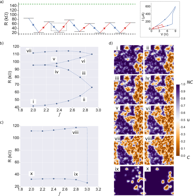
Figure 4b illustrates a simulated sweep starting from a microstructure that is predominantly in the NC phase. Examples of the simulated microstructures generated during the sweep are given in Figure 4d, panels (i-vii). As is increased, some of the pinning centers are depinned, causing the volume fraction of the C phase (orange domains in Figure 4d) to increase, and resulting in an increase in the bulk resistance. When is swept back to its initial value, the state the system returns to is different than its initial state, as the steady-state solution depends on both the value of and on the history of the material. Figure 4c demonstrates a sweep starting from the predominantly C phase from Figure 4d, panel (vii). Once is increased to , NC domains form around clusters of pinning centres (Figure 4d panel (ix)). The state of the system when is returned to its initial value has a significantly larger volume fraction of NC regions compared to the initial microstructure, and thus a lower resistance.
In summary, we used STM to image ultrathin flakes of 1T-\chTaS2 in the hysteresis region of the NC-C phase transition. The exfoliated flakes, with lateral dimensions , were integrated into a device design that allows for the observation of changes in the electronic structure of the material that accompany changes in bulk electrical properties. Within the hysteresis region of the NC-C phase transition, we found ultrathin 1T-\chTaS2 to exist in a state with electronic inhomogeneity, indicative of the competition between different equilibrium states. This result highlights the complexity in the phase diagram of 1T-\chTaS2 and demonstrates the importance of understanding the characteristics of its phase competition morphologies in order to identify potential applications for this material.
References
- Dagotto (2005) Dagotto, E. Science 2005, 309, 257–262.
- Battisti et al. (2017) Battisti, I.; Bastiaans, K. M.; Fedoseev, V.; De La Torre, A.; Iliopoulos, N.; Tamai, A.; Hunter, E. C.; Perry, R. S.; Zaanen, J.; Baumberger, F.; Allan, M. P. Nature Physics 2017, 13, 21–25.
- Sun et al. (2021) Sun, Z.; Guevara, J. M.; Sykora, S.; Pärschke, E. M.; Manna, K.; Maljuk, A.; Wurmehl, S.; van den Brink, J.; Büchner, B.; Hess, C. Physical Review Research 2021, 3, 023075.
- Fradkin et al. (2015) Fradkin, E.; Kivelson, S. A.; Tranquada, J. M. Reviews of Modern Physics 2015, 87, 457.
- Uehara et al. (1999) Uehara, M.; Mori, S.; Chen, C.; Cheong, S.-W. nature 1999, 399, 560–563.
- Wilson et al. (1975) Wilson, J. A.; Di Salvo, F.; Mahajan, S. Advances in Physics 1975, 24, 117–201.
- Ritschel et al. (2015) Ritschel, T.; Trinckauf, J.; Koepernik, K.; Büchner, B.; Zimmermann, M. v.; Berger, H.; Joe, Y.; Abbamonte, P.; Geck, J. Nature physics 2015, 11, 328–331.
- Sipos et al. (2008) Sipos, B.; Kusmartseva, A. F.; Akrap, A.; Berger, H.; Forró, L.; Tutiš, E. Nature materials 2008, 7, 960–965.
- Ma et al. (2016) Ma, L.; Ye, C.; Yu, Y.; Lu, X. F.; Niu, X.; Kim, S.; Feng, D.; Tománek, D.; Son, Y.-W.; Chen, X. H.; Zhang, Y. Nature communications 2016, 7, 1–8.
- Cho et al. (2016) Cho, D.; Cheon, S.; Kim, K.-S.; Lee, S.-H.; Cho, Y.-H.; Cheong, S.-W.; Yeom, H. W. Nature communications 2016, 7, 1–6.
- Stojchevska et al. (2014) Stojchevska, L.; Vaskivskyi, I.; Mertelj, T.; Kusar, P.; Svetin, D.; Brazovskii, S.; Mihailovic, D. Science 2014, 344, 177–180.
- Vaskivskyi et al. (2016) Vaskivskyi, I.; Mihailovic, I.; Brazovskii, S.; Gospodaric, J.; Mertelj, T.; Svetin, D.; Sutar, P.; Mihailovic, D. Nature communications 2016, 7, 1–6.
- Yu et al. (2015) Yu, Y.; Yang, F.; Lu, X. F.; Yan, Y. J.; Cho, Y.-H.; Ma, L.; Niu, X.; Kim, S.; Son, Y.-W.; Feng, D.; Li, S.; Sang-Wook, C.; Chen, X. H.; Yuanbo, Z. Nature nanotechnology 2015, 10, 270–276.
- Patel et al. (2020) Patel, T.; Okamoto, J.; Dekker, T.; Yang, B.; Gao, J.; Luo, X.; Lu, W.; Sun, Y.; Tsen, A. W. Nano Letters 2020, 20, 7200–7206.
- Hollander et al. (2015) Hollander, M. J.; Liu, Y.; Lu, W.-J.; Li, L.-J.; Sun, Y.-P.; Robinson, J. A.; Datta, S. Nano letters 2015, 15, 1861–1866.
- Yoshida et al. (2015) Yoshida, M.; Suzuki, R.; Zhang, Y.; Nakano, M.; Iwasa, Y. Science advances 2015, 1, e1500606.
- Ma et al. (2019) Ma, Y.; Wang, Z.; Hou, Y.; Wu, D.; Lu, C.; Petrovic, C. Physical Review B 2019, 99, 045102.
- Ludwiczak et al. (2020) Ludwiczak, K.; Lacinska, E.; Binder, J.; Lutsyk, I.; Rogala, M.; Dabrowski, P.; Klusek, Z.; Stepniewski, R.; Wysmolek, A. Solid State Communications 2020, 305, 113749.
- Frenzel et al. (2018) Frenzel, A. J.; McLeod, A. S.; Wang, D. Z.-R.; Liu, Y.; Lu, W.; Ni, G.; Tsen, A. W.; Sun, Y.; Pasupathy, A. N.; Basov, D. Physical Review B 2018, 97, 035111.
- Tsen et al. (2015) Tsen, A. W.; Hovden, R.; Wang, D.; Kim, Y. D.; Okamoto, J.; Spoth, K. A.; Liu, Y.; Lu, W.; Sun, Y.; Hone, J. C.; Kourkoutis, L. F.; Kim, P.; Pasupathy, A. N. Proceedings of the National Academy of Sciences 2015, 112, 15054–15059.
- Wu and Lieber (1989) Wu, X. L.; Lieber, C. M. Science 1989, 243, 1703–1705.
- Thomson et al. (1994) Thomson, R.; Burk, B.; Zettl, A.; Clarke, J. Physical Review B 1994, 49, 16899.
- Burk et al. (1991) Burk, B.; Thomson, R.; Zettl, A.; Clarke, J. Physical review letters 1991, 66, 3040.
- Wu and Lieber (1990) Wu, X. L.; Lieber, C. M. Physical review letters 1990, 64, 1150.
- Tanda et al. (1984) Tanda, S.; Sambongi, T.; Tani, T.; Tanaka, S. Journal of the Physical Society of Japan 1984, 53, 476–479.
- Tanda and Sambongi (1985) Tanda, S.; Sambongi, T. Synthetic metals 1985, 11, 85–100.
- McMillan (1976) McMillan, W. L. Physical Review B 1976, 14, 1496.
- Nakanishi et al. (1977) Nakanishi, K.; Takatera, H.; Yamada, Y.; Shiba, H. Journal of the Physical Society of Japan 1977, 43, 1509–1517.
- Nakatsugawa et al. (2020) Nakatsugawa, K.; Tanda, S.; Ikeda, T. N. Scientific reports 2020, 10, 1–9.
- Zong et al. (2018) Zong, A.; Shen, X.; Kogar, A.; Ye, L.; Marks, C.; Chowdhury, D.; Rohwer, T.; Freelon, B.; Weathersby, S.; Li, R.; Yang, J.; Checkelsky, J.; Wang, X.; Nuh, G. Science advances 2018, 4, eaau5501.
- (31) Chaikin, P. M.; Lubensky, T. C. Principles of condensed matter physics; Vol. 10.
- Dagotto et al. (2001) Dagotto, E.; Hotta, T.; Moreo, A. Physics reports 2001, 344, 1–153.
- Hohenberg and Halperin (1977) Hohenberg, P. C.; Halperin, B. I. Reviews of Modern Physics 1977, 49, 435.
- Frank and Lobb (1988) Frank, D.; Lobb, C. Physical Review B 1988, 37, 302.
Acknowledgements.
The authors thank Neil Curson and Joseph Salfi for helpful discussions. This research was undertaken thanks in part to funding from the Canada First Research Excellence Fund. J.O. acknowledges the support by Georg H. Endress Foundation. JJG, X.L., WJL and Y.P.S. thank the financial supports from the National Natural Science Foundation of China under Contract Nos. 11674326, 11874357, the Joint Funds of the National Natural Science Foundation of China, the Chinese Academy of Sciences’ Large-Scale Scientific Facility under Contract Nos. U1832141, U1932217, and U2032215, the Key Research Program of Frontier Sciences, CAS (No. QYZDB-SSW-SLH015), the uses with Excellence and Scientific Research Grant of Hefei Science Center of CAS (No.2018HSC-UE011). A.W.T. acknowledges support from the US Army Research Office (W911NF-21-2-0136), Ontario Early Researcher Award (ER17-13-199), and the Natural Science and Engineering Research Council of Canada (NSERC) (RGPIN-2017-03815).I Supplementary Material for “Observation and manipulation of a phase separated state in a charge density wave material”
I.1 Fabrication Details
I.1.1 Synthesis of 1T-\chTaS2
Single crystals of 1T-\chTaS2 were grown by chemical vapor transport with iodine as the transport agent. High-purity \chTa ( N) and \chS ( N) were mixed in chemical stoichiometry and heated at for days in an evacuated quartz tube. The harvested \chTaS2 powders and iodine (density: ) were then sealed in another quartz tube and heated for weeks in a two-zone furnace, where the source and growth zones were held at and , respectively. The tubes were then rapidly quenched in cold water to retain the 1T phase.
I.1.2 Electrode fabrication
Electrodes were fabricated on an \chSiO2 ( nm)/\chSi substrate. Standard electron beam lithography and e-beam metal deposition techniques were used to fabricate pads of \chAu ( nm)/\chTi ( nm). An array of size markers (\chAu ( nm)/\chTi ( nm)) spaced apart was deposited on top of the pads. The pads were contacted by larger contacts of \chAu ( nm)/\chTi ( nm), fabricated using mask-less photolithography and e-beam deposition.
I.1.3 2D material transfer procedure
To prevent oxidation of the 1T-\chTaS2 flakes the exfoliation and transfer of 2D materials was done inside a \chN2 filled glovebox with \chO2 and \chH2O partial pressures below ppm. The materials were exfoliated and transferred sequentially on top of each other using the following method:
-
1.
A bulk crystal of the 2D material is exfoliated onto a piece of Scotch tape.
-
2.
A polypropylene carbonate (PPC) thin film is prepared by spin coating ( RPM, sec) PPC in an anisole solution ( PPC by weight) on a glass cover slide. The Scotch tape with the exfoliated flakes is pressed onto the thin film of PPC and then peeled off.
-
3.
The PPC thin film is transferred onto a polydimethylsiloxane (PDMS) stamp sitting on a glass slide.
-
4.
A home-built setup utilizing a motorized arm attached to a microscope is used to identify a suitable flake on the PPC film.
-
5.
The selected flake is aligned with the fabricated electrodes as desired and brought into contact with the substrate. The substrate is then heated to , causing the PPC to melt and peal off of the glass slide at the point of contact, transferring the flake and PPC film to the substrate.
-
6.
The heater is switched off and the electrodes with the transferred flake and PPC are put into a vacuum chamber for min. before the PPC is washed away in a chloroform bath, leaving only the flake on the substrate.
-
7.
The sample is then rinsed with acetone and isopropanol.
I.1.4 STM measurements
All STM measurements were performed with an Omicron LT-STM outfitted with four electrical contacts. STM topography was taken in constant-current mode with the bias applied to the tip. The samples were heated to prior to being transferred to the STM chamber.
Ultrathin flakes of 1T-\chTaS2 are difficult to image with STM due to the instability of the material in air as well as the requirement that the sample not be heated above , as that would cause the TMD to undergo a structural phase transition to the 2H polytype. However, despite the processing difficulties described above and the exposure of the samples to various chemicals during fabrication, the exfoliated flakes we measured remained sufficiently free of contaminants to resolve the CDW superstructures characteristic of the bulk phases of 1T-\chTaS2.
I.2 Chiral states
As 1T-\chTaS2 undergoes a phase transition from the incommensurate (IC) charge density wave (CDW) phase to the nearly commensurate (NC) CDW phase two chiral orientations are possible. In the IC phase the CDW wave vector is oriented along the atomic lattice wave vector while in the NC phase the CDW is rotated away from the atomic lattice at an angle that is dependent on the temperature of the system (). The two possible chiral orientations correspond to whether the CDW is rotated either clockwise or counterclockwise.
Both orientations are equivalent and have been observed to exist within the same sample.Zong et al. (2018) Furthermore, interconversion between the different orientations has been shown via femtosecond laser pulses.Zong et al. (2018). We observe the coexistence of the two chiral phases separated by a mirror twin boundary.
I.3 Further electrical characterization
In this section, transport measurements are presented for two 1T-\chTaS2 samples of a similar thickness, , hereby called Sample A, and Sample B. Sample A was the device imaged in Figures 2 and 3 in the main text, while Sample B is the device driven in Figure 4d and 4e.
The resistance of the device was measured using a four-terminal, constant current circuit that does not exclude the contact resistance. For all DC voltage sweeps, a Keithley Source Measurement Unit (Keithley 2401 or Keithley 2450) was used to apply the bias voltage and to measure the resulting current. For the traces plotted in Figure 6, the DC sweep rate was . AC measurements were performed with a SR830 lockin, with a signal frequency of . The circuit included a current divider in order to protect the lockin from excessive current.
As evidenced in Figure 4b from the main text, multiple sweeps to the same voltage value will continuously manipulate the state of the material. Assuming the maximum voltage set is less than the voltage at which breakdown of the C domains occurs, the material will be driven to some intermediate state with a higher resistance compared to the initial state. With this consideration in mind, applying a lateral AC bias across the sample will drive the material more efficiently than a DC bias, as when using an AC signal multiple sweeps are performed. Figure 7 demonstrates this behavior.
Using an AC bias at , the sample is driven to the saturation resistance level more directly, and at lower voltages compared to when a DC bias is used. Whether there exists an alternative explanation for the enhancement observed when using an AC voltage, one that is based upon the underlying microscopic mechanism that facilitates the electrical driving, is beyond the scope of this work.
I.4 Time-dependent Ginzburg-Landau theory
We aim to provide some qualitative insight into the phase separation dynamics using time-dependent Ginzburg-Landau (TDGL) theory. While the main results of the simulations were provided in the main text, this section contains further details of the modeling.
The governing equation in TDGL is:Hohenberg and Halperin (1977)
| (3) |
where is a damping parameter. Starting from a Landau free energy with minima at (the C phase) and (the NC phase) we introduce the phenomenological parameter to tune the stability of the C phase relative to the NC phase by tilting the free energy potential:
| (4) |
where controls the magnitude of the energy barrier between the C phase and the NC phase, and the energy is measured in units of the elastic energy.
Starting from a random, inhomogeneous microstructure, the system is allowed to evolve according to Equation 3. Without introducing disorder, the system will form either the homogeneous C or NC phase, depending on the value of the tilt parameter, . However, if disorder is introduced into the model in the form of pinning centers, impurity sites where the order parameter is reset to at the end of each time step, a phase separated structure containing intertwined C and NC phase domains is generated. The NC domains are situated around clusters of pinning centers, and the relative volume fractions of the two phases depend on both and the total number of impurity sites introduced (Figure 9a). A 5-point Laplacian discretization is used in solving Equation 3. For all of the presented simulations, the impurity concentration was set to and the system was allowed to equilibrate over time steps at each value of .
In order to simulate the electrical driving we model the system as a 2D resistor network with NC and C nodes. Initially, the system is considered to be in a state with a small C phase volume fraction, as depicted in Figure 10a.
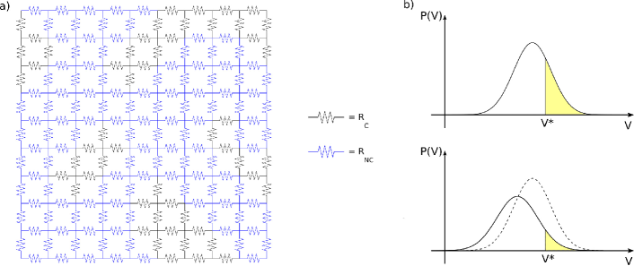
Due to the coexistence of the C and NC phase domains, the voltage applied across the sample will not drop homogeneously but will depend on the geometric arrangement of the microstructure. Consequently, the voltage drop across the complete set of NC regions will have some distribution . An applied electric field stabilizes the C phase relative to the NC phase. With respect to the model, this effect corresponds to an increase in the parameter . As a voltage is applied to the sample, the voltage drop across some of the NC nodes exceeds a certain critical value resulting in those NC nodes in the resistor network to become C. When this conversion occurs the distribution of the voltage across the NC nodes changes (Figure 10b).
The general picture described above is approximated in the simulations by introducing a limiting value below which the order parameter is depinned from an impurity site, meaning it is not reset to at the end of each time step. With this modification, the final microstructure generated from the time evolution of the system becomes dependent on the initial C phase volume fraction, , in addition to the tilting parameter and the number of pinning centers. For small values of (, the system evolves to a percolated NC phase, with a resistivity comparable to that of the homogeneous NC phase, while for larger , the system goes to the C phase. This result is demonstrated in Figure 9b, where the resistance of the generated microstructure is calculated for different sets of values of and . The driving model is completed by adding a second set of threshold parameters, and , to control the conversion of C nodes to NC nodes. When , nodes where the order parameter is greater than are converted to , the NC phase.
The model described above does not explicitly allow for the rearrangement of the NC and C domains as the location of the pinning centres essentially fixes the geometric arrangement of the microstructure. Thermal noise and Joule heating effects stemming from the flow of charge carriers are not included, but would result in a more complete picture that might allow for the possibility of the rearrangement of the microstructure. Despite this limitation, the model does recreate many of the essential features of the observed driving.