A Superconducting Nanowire-based Architecture for Neuromorphic Computing
Abstract
Neuromorphic computing would benefit from the utilization of improved customized hardware. However, the translation of neuromorphic algorithms to hardware is not easily accomplished. In particular, building superconducting neuromorphic systems requires expertise in both superconducting physics and theoretical neuroscience, which makes such design particularly challenging. In this work, we aim to bridge this gap by presenting a tool and methodology to translate algorithmic parameters into circuit specifications. We first show the correspondence between theoretical neuroscience models and the dynamics of our circuit topologies. We then apply this tool to solve a linear system and implement Boolean logic gates by creating spiking neural networks with our superconducting nanowire-based hardware.
I Introduction
Neuromorphic computing attempts to mimic the behavior of biological neurons and synapses in the human brain. Recently, increased understanding of the physics of devices for neuromorphic computing [1, 2], and the theory of algorithms for neuromorphic computing [3] has led to the development of CMOS-based neuromorphic architectures [4] that are three orders of magnitude more efficient in terms of their energy-delay product when compared to traditional multiply-and-accumulate operations [5]. However, these systems are also nowhere near the power figure of merit (energy per operation) required to create a massive scale neuromorphic computer, such as the human brain.
For these reasons, efforts to mimic neurons and synapses may need to move towards systems that have an intrinsic spiking ability and extremely low energy consumption. This is the case in superconducting electronics where the constituent elements exhibit nonlinear characteristics and have very low or no power dissipation. Superconducting circuits offer drastically lower power consumption even when cryogenic cooling energy costs is taken into account [6, 7]. Previous developments of neuromorphic architectures using superconducting electronics have used Josephson junctions [8, 9, 10, 11], quantum-phase slip junctions [12, 13, 14], magnetic tunnel junctions [15], systems with Josephson junctions and superconducting nanowire single photon detectors [16, 17], and nanowires as relaxation oscillators [7] to construct circuits that emulate biological neurons and synapses. Superconducting nanowires offer ease of fabrication and are most easily integrated with classical circuit elements. In addition, the ability of superconducting circuits to operate with near-lossless interconnects makes them an attractive choice for implementing a low-power neuromorphic architecture.
Simultaneously, the success of Artificial Neural Networks (ANNs) [18] in computing applications such as pattern recognition and natural language processing coupled with the widespread adoption of machine learning methods in many areas of science and engineering is an indication that abstracting a computing problem and eliminating hardware dependencies is a promising approach for going beyond Moore’s law. Among these networks, Spiking Neural Networks (SNNs) closely simulate the dynamics of biological neurons and synapses in the brain. Approaches to spiking neural networks that possess brain-like properties have gained increased attention due to their widespread use in applications spanning decision making [19], image recognition [20] and optimization problems [21].
The direct translation of superconducting neuromorphic architectures into algorithmic formulations of a problem has been little explored, and a complete description of an algorithmic implementation in neuromorphic hardware remains to be seen. It is very difficult for hardware designers to condense an abstract algorithmic problem into a specific hardware platform without increasing the complexity of circuits or compromising energy efficiency. This gap in the field stems from the difficulty in reconciling the algorithmic and hardware oriented approaches. At this point in time, this issue is often a question of expertise: hardware designers do not have ready knowledge of algorithmic subtleties, while algorithm developers do not have access to the hardware. Thus, there is a need for a tool to allow computer scientists to test algorithms on neuronal circuits. We devise and present such a tool here.
In this work, we address the issue of translation from theoretical algorithms to a specific implementation by using the example of solving linear systems with a superconducting neuromorphic network. We show the direct relation between a basic compositional model as well as a leaky integrate-and-fire model and the proposed superconducting nanowire-based neuromorphic hardware. We compile this correspondence into a tool to translate between hardware and algorithmic descriptions of the neuromorphic architecture. We conclude with a discussion on the outlook of the scaling of superconducting nanowire-based circuits in the context of neural networks.
II Methods
The building blocks of the hardware architecture are superconducting nanowires [22] and hTrons [23]. In a superconducting nanowire biased with a current, superconductivity breaks down when the current when the current exceeds the critical current . As a consequence, the nanowire develops a resistance and a voltage . Superconductivity is restored in the nanowire when its current is reduced below the retrapping current . When a superconducting nanowire is placed in parallel with a resistor, the relaxation from the normal to the superconducting state of the nanowire can couple with the resistor. When biased by a current above , the nanowire switches and electrothermal feedback produces continuous voltage spikes across the nanowire. This is termed a relaxation oscillator [24].
The hTron is a circuit element that acts as a thermally activated switch. It consists of a superconducting nanowire (the channel), placed in close proximity to a resistive element (the gate) [23]. When the channel is biased by a current below its threshold , heat dissipated by the gate can increase the temperature of the channel and break superconductivity. Superconductivity is restored in the channel when it has cooled and its current is reduced below a threshold . This threshold is dependent on the temperature of the channel and decreases for increasing temperature [23].
The simulations used in this work are based on models for superconducting nanowires [22] and for hTrons [23] implemented in LTSPICE [25].
II.1 Hardware Design
In previous work [7], the application of two superconducting nanowires whose intrinsic nonlinear inductance was used to generate spiking behaviour is presented. We summarize the description here.
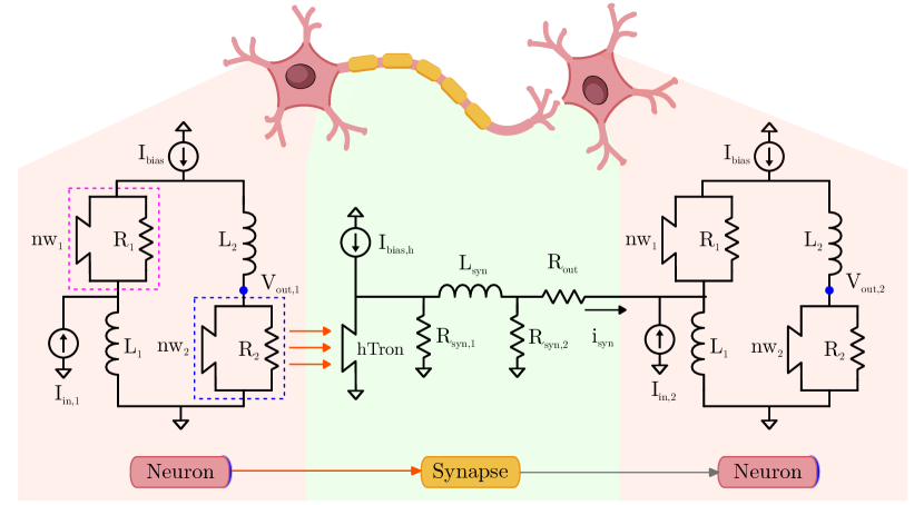
As illustrated in Figure 1, the nanowire neuron consists of a main and control relaxation oscillator in a loop. A source biases both oscillators below their critical currents but in opposite directions. An input current pulse at applied to the loop then results in the current in the main oscillator to exceed , causing it to switch. Then, current is diverted counterclockwise in the loop which causes the control oscillator to switch while the main oscillator relaxes. The switching of the control oscillator diverts current clockwise and causes the main oscillator to switch again. Each time main oscillator switches, a voltage spike will be seen at node . The main and control oscillator act analogously to the Na+ and K+ ion channels in the Hodgkin-Huxley neuron model [26].
The synapse consists of an hTron and an integration loop formed by , and . When a voltage spike appears at , heat is dissipated across (orange arrows). acts as the gate of the hTron, and the heat from it lowers the critical current of the hTron channel, causing the hTron to switch. In the switched (normal, non-superconducting) state, the resistance of the channel is typically on the order of for NbN films. The typical resistance for and is on the order of . Thus, when the hTron channel switches, the majority of the current is diverted into the integration loop. A portion of the current through is then transmitted to the target neuron via . This process is analogous to the integration behaviour of the Hodgkin-Huxley model [26].
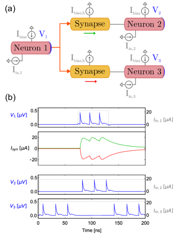
The simulated operation of a simple neuron-synapse-neuron connection demonstrating excitatory and inhibitory behavior is shown in figure 2. The network illustrated consists of an input neuron (1) connected to two target neurons (2,3). The spike output from neuron 1 is connected thermally to the synapses via the hTron and the synapses are connected electrically to neuron (2,3). When makes neuron 1 fire, the spikes are integrated in the synapse as shown by in figure 2b. This synaptic current leads to the excitation of neuron 2 for a brief period of time. Similarly, the same current but in the opposite direction leads to inhibition of the firing of neuron 3 for a brief period of time.
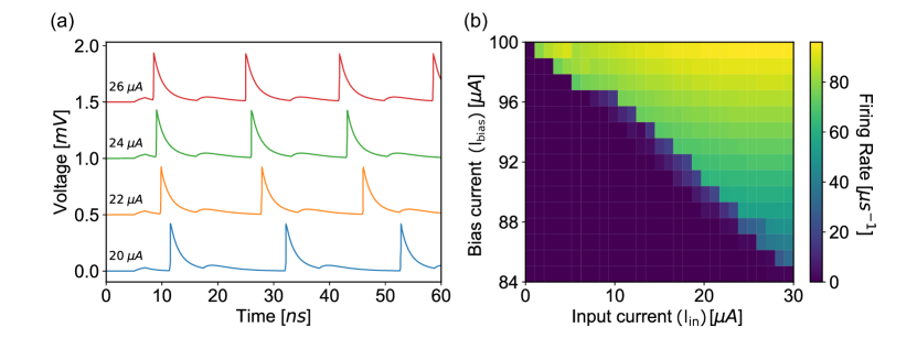
In spiking neural networks, information must be encoded in the timing of the spikes in the network. In figure 3, we demonstrate the time-domain response of the neuron circuit with respect to its current biasing conditions. We define the spike period as the time between the voltage spikes in a neuron. Figure 3a demonstrates a decrease in the spike period of the nanowire neuron as a function of increasing input current. This same behaviour is seen in overbiased relaxation oscillators, where biasing a nanowire above its critical current also results in frequency-tunable oscillations [27]. We map the effect of this current-controlled frequency-tunability in figure 3b. From the color map a firing threshold for the nanowire neuron can be identified from the summation of the input and bias currents. Once this threshold is reached, either an increase in the bias current or an increase in the input current result in an increase in the firing rate. This behavior can be explained from the critical current dynamics of the nanowires in the neuron circuit.
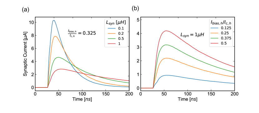
Similarly, the synapse circuit presented in figure 1 also demonstrates tunable characteristics. The integration loop of the synapse acts as a leaky integrator circuit. The time-domain response of this circuit can be set during its design, by choosing the ratio between the time constant and the time constant, where is the inductance of . The leakiness of the synapse is illustrated in figure 4a where the current in the synaptic inductor is plotted for different values of synaptic inductance. In addition, controls the amount of current injected into the integration loop, modifying the output of the synapse. Therefore, the strength of the synaptic connection can be updated externally by tuning . Figure 4b shows the output current of the synapse for different values of .
III Results
To connect our hardware with the computational picture of a neural network, we developed two mappings from hardware to mathematical models. First is a mapping between the physical system described in the previous section and the well-known leaky integrate-and-fire neuronal model [28], second is the mapping to a recently developed compositional model for spiking neural networks [3].
III.1 Correspondence
III.1.1 Correspondence to Leaky Integrate-and-fire Model
The Leaky integrate-and-fire neural network is one of the most commonly studied network-level models in neuroscience. In a network of neurons, each is associated with a time-varying potential value. In this model, a neuron’s potential is governed by the following equation:
| (1) |
where represents the potential of the ith neuron at time ; is the initial potential with no input; and is the external input to the neuron. The leaky integration dynamic is encapsulated in the leakiness parameter of the neuron, that is the rate at which the neuron potential decreases. The synaptic strength from a neuron to a neuron is represented by matrix coefficient and a transfer parameter . The spiking events of neuron occur according to the following spike rule :
| (2) | ||||
where is the threshold potential. We relate the parameters of this model to our superconducting hardware as described below.
In our hardware, the current in the nanowire of the neuron’s main oscillator corresponds to the potential in the leaky integrate-and-fire model. In the nanowire-based implementation, the spike rule corresponds to the voltage in the nanowire, the spiking events of the nanowire neuron are described by the following spike rule:
| (3) | ||||
This relatively natural correspondence is what makes the superconducting system particularly elegant for the implementation of spiking neural networks.
Similarly, the initial potential directly corresponds to the initial value of . For instance, when the inductance and resistance values between the two branches of the neurons are the same, the bias current in the nanowire of the main oscillator will be .
Moreover, the integration behaviour of the model corresponds to the ability of the hTron synapses to integrate the voltage spikes generated by the upstream neurons. The switching of the hTron channel and its subsequent diversion of current into the integration loop of the synapse, can be approximated by a leaky integration circuit with dynamics described by:
| (4) |
Continuing with the analogy, the leakiness parameter corresponds to the ratio of the time constant of the relaxation of the nanowire in the neuron to the time constant of the integration loop in the synapse . can be set such that it is larger than to allow the synapse to retain the spike information from the neurons.
The transfer parameter in the model corresponds to the ratio between and the current entering the nanowire of the main oscillator. The value of is dependent on the number of synapses connected to a neuron, the synaptic inductance, and the inductances and of the nanowire neuron. For a neuron with a large number of synapses connected to its input terminal, less current from each synapse enters the neuron.
The matrix coefficients correspond to between the ith and jth neurons as it represents the strength of the connection between two neurons via a synapse. In the hardware, can be externally tuned as discussed in the previous section and illustrated in figure 4. Coupled together, can be mapped to the current added to the nanowire of the main oscillator.
The terms in the model correspond to the external input current source to the ith neuron as shown in figure 1.
III.1.2 Correspondence to a Basic Compositional Model
An algorithmic model for spiking neural networks has been recently introduced.[3] The model lays out a schema to track a set of neurons (nodes) with a set of synapses (edges) , in a graph by recording a potential for each neuron, at some discrete time.
-
•
In the model, a neuron can be in one of two states: firing and not firing. For a neuron at node we have when the neuron is firing and when not firing. We call this function the configuration of a neuron.
-
•
The connection between a neuron and neuron via a synapse is encapsulated in a function .
-
•
At discrete time , every neuron has a potential .
-
•
The firing rule for the neuron is probabilistic and is described by . Here is distinct from the leakiness parameter of the leaky integrate-and-fire model and is instead an arbitrary real temperature parameter.
The neuron biasing condition is akin to the currents and into a neuron as in figure 1. We associate the neuron biasing condition to be the location as in figure 3b.
The configuration of a neuron corresponds to the state of the nanowire of the main oscillator of the neuron. When the nanowire switches, the neuron is firing. Conversely, when the nanowire is in the superconducting state the neuron is not firing.
The weight of a synapse between two neurons is mapped to of the synapse between them. As in the leaky integrate-and-fire model, this weight can be externally tuned as demonstrated in figure 4.
The potential of the neuron can be associated with the current in the nanowire of the main oscillator . As shown in figure 1, this current dependent on the on and and is affected by the current coming from the connections of other synapses.
The firing rule can be associated with the switching of the nanowire in the main oscillators. While it is true that the nanowire switches whenever , this is probabilistic in a physical implementation and is dependent on and . The firing probability as a function of and was explored in experiments with nanowire neurons here [29].
We summarize the correspondence between the two models presented and the physical parameters in the table I and II.
| Leaky integrate-and-fire model | Physical Model |
|---|---|
| Initial potential of a neuron | Initial current in the nanowire, |
| Spike function | Voltage spikes at |
| Connection between neurons, | Bias current in the synapse |
| Potential of a neuron, | Current in the nanowire of the main oscillator |
| Spike rule | Nanowire switches when with noise |
| Leakiness parameter, | Time constants of the neuron and synapse |
| Compositional Model | Physical Model |
|---|---|
| Bias conditions of a neuron, | and in figure 3 |
| Configuration of a neuron, | Voltage spikes at |
| Weight of a synapse, | Bias current in the synapse, |
| Potential of a neuron | Current in the nanowire of the main oscillator |
| Firing probability, | Nanowire switches when with noise |
III.2 Model and Translational Tool
From the above descriptions of the leaky-integrate-and-fire model and the basic compositional model for spiking neural networks, we built a tool to directly relate the parameters of the models to the physical implementation of the nanowire neuron and synapse. This tool can help bridge the expertise gap between computer scientists and hardware engineers in designing neuronal circuits as it provides a platform for a common description of a problem.
III.2.1 Implementation of the Translational Tool
In the tool, the network consisting of the neurons and synapses is described as a graph. A vector V describing the bias conditions to the neurons (the vertices) and a matrix E describing the strength of the synapses between them (the edges) is specified. Then, the algorithmic description from the leaky integrate-and-fire model, or the compositional model is chosen. Depending on the choice of model, V is treated as or and E is treated as or . Correspondingly, the parameters of the algorithmic model are tuned either at each individual node or across the whole graph. The tool translates the parameters of each algorithmic model to the low-level hardware description based on the correspondence between the parameters described in each the previous section.
The tool uses SciPy’s numerical solver IVP [30] to simulate the underlying system based on a state variable description of the nanowire neuron circuit, as follows:
| (5) |
in this case, is a nonlinear function accounting for the kinetic inductance of the nanowire following the expression from [22]. We define the current as where is the current flowing through from each synapse to the neuron and is as in figure 1. The remaining current variables are further defined in the appendix.
Note that here we make a simplifying assumption about the dynamics of a superconducting nanowire. We specify a state variable for each nanowire to capture whether the nanowire is in the superconducting or the normal state. The transition from the superconducting to the normal state is brought about when . The transition form the normal state back to the superconducting state occurs when .
Similarly, a state-variable description for the synapse is as follows:
| (6) |
We use the same simplifying assumption about the dynamics of the channel of the hTron as we use for the nanowires in the neuron. Transitions to the normal state in the channel of the hTron are brought about after its current surpasses and its return to the superconducting state occurs when its current is below . To couple neuron and the synapse, we force the hTron channel to switch everytime the neuron fires, that is we set whenever . In an effort to facilitate broad use of this model, we reference the code implementing it here 111https://github.com/qnngroup/neuron.
As an example, using the tool to relate a leaky integrate-and-fire model to the hardware, the following steps are taken to translate the algorithmic description to the hardware:
-
1.
The neurons and the synapses between them are configured as specified by the user in their graph description
-
2.
By default, the internal parameters of a neuron are set to typical values as are the parameters of a synapse
are set to . -
3.
and are respectively mapped directly to in the neuron and of the nanowires.
-
4.
is set such that the leakiness parameter .
-
5.
For each synapse, is set such that the current in increases by a factor of . This ratio is maintained across all synapses. Correspondingly, is set to be higher than .
-
6.
External inputs to the neurons are proportionally mapped to the input currents of each neuron.
-
7.
The network is simulated by solving the IVP’s of underlying circuits.
In the following section apply the correspondence of our hardware to two algorithmic examples. We simulate Boolean gates and solve special linear systems with our superconducting-nanowire-based neuromorphic architecture. These choices stem from the ubiquitous nature of Boolean gates and algorithms to solve linear systems in classical computing.
III.3 Solving Linear Systems
In a recent paper by Chou et al. [32], non-leaky integrate-and-fire neural networks were shown to efficiently solve linear systems. Here, we demonstrate the computational power of SNNs in simulation by implementing their theoretical models using our superconducting nanowire-based architecture. As a proof of concept, we start with solving a simple two-dimensional linear system. Then, we scale up the problem to a five-dimensional linear system with Laplacian structure.
The motivation for Laplacian linear systems is two-fold: (1) many practical applications and engineering problems rely on solving large Laplacian linear systems such as diffusion models, graph models and random walks; (2) some Laplacian linear systems have infinitely many solutions. Chou et al. [32] predicted that a SNN will converge to the solution with the least vector magnitude. We use the approach taken by Chou et al. [32] to solve Laplacian linear systems, namely a 22 and a 55 system.
To translate a linear system of the form to a SNN, we map to be the elements of the matrix and to be the vector to ensure that the matrix is positive semidefinite (PSD). The number of neurons in the SNN corresponds to the dimension of .
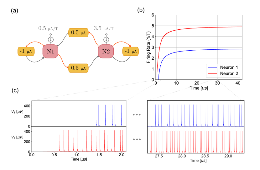
For the first example, we attempt to solve the following linear system which is already PSD:
| (7) |
We illustrate the network for solving this system and use the tool to handle parameter mapping as in figure 5. The connectivity matrix from the leaky integrate-and-fire model corresponds to the matrix in the problem. We can then map the elements of matrix from the problem to the weights of the synapses as shown in figure 5a. Similarly, the row elements of vector are mapped to the ramp rates of currents at for each of the neurons relative to the timescale of the neuron. To apply the leaky integrate-and-fire model, we set the timescale of integration to ensure that the current in the synapse decays much slower relative to the decay of current after a neuron spike. Using the tool, we chose and .
The evolution of the system is illustrated in figure 5c. Initially, neither neuron is firing. As time progresses, the input current to each neuron increases at different rates. Since the external bias for neuron 2 is greater, its potential will increase faster and it will fire earlier. When neuron 2 fires, both of its outgoing synapses are activated. Neuron 2 excites neuron 1 but also inhibits itself. After some time, neuron 1 will fire as a result of the excitation from neuron 2. When neuron 1 fires, it will excite neuron 2 but inhibit itself. As can be seen in figure 5b, two distinct firing rates emerge from the system. Specifically, we reference the approach of Chou et al. [32] to define a firing rate as:
| (8) |
where is the cumulative number of spikes at time . As can be seen in figure 5b, we find that the firing rate of each neuron converges to the rows of the solution vector of the linear system .
To illustrate the generality of the method, we extend the approach to solving a more complex linear system. We apply the same approach to solving a cycle graph represented by the following linear system which is again already PSD:
| (9) |
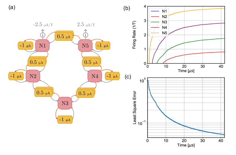
We can map again the elements of matrix to the connectivity matrix and the elements of vector to the input currents of the neurons. We use the tool described in the previous section to simulate the system and illustrate the results in figure 6.
These results can be understood from an energy minimization perspective. When neuron 5 fires, it will excite neuron 4 after a long period of time. When neuron 4 begins firing continuously, neuron 3 will be excited. This same effect will propagate to neuron 2 after a period of time. Neuron 1 will not fire due to the fact that the input current to the neuron is negative. This is illustrated in figure 6b where the firing rates of the different neurons have different activation times. It must then be noted that this linear system defined by the cycle graph has multiple solutions and the firing rate of our SNN approaches the solution with the least L1 norm as predicted in [32]:
To assess the evolution of the network and determine error in the firing rate, we defined the least square error as follows:
| (10) |
Where the notation signifies the magnitude of the vector. We take to be the instantaneous firing rate vector. We plot the evolution of the least square error in figure 6c.
III.4 Boolean Gates
We also implement several Boolean gate network examples found in Lynch and Musco’s paper [3]. The networks were created using their algorithmic model and then translated into our neuromorphic hardware. Boolean gates are relevant algorithmic examples to convert into neuromorphic computing hardware given their high importance in classical computing and their use in neural networks. Thus, neuromorphic versions of a universal set of Boolean gates could enable computation with both classical and neuromorphic paradigms.
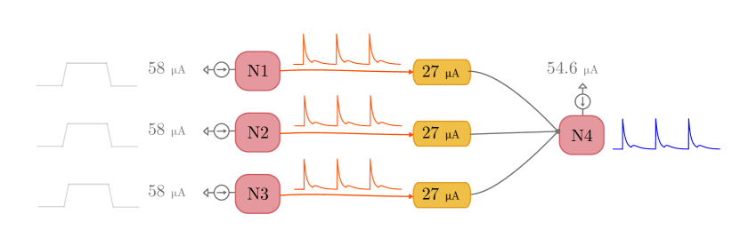
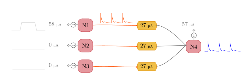
We demonstrate a 3-input AND gate network in figure 7. In the following paragraph, we describe the operation of this network using the compositional framework from Lynch and Musco’s paper [3]. We understand the operation of the network using the compositional model. The weight of the synapses are taken to be . When all three of the input neurons fire, the potential of the neuron is and the probability of the output neuron firing is . When only two input neurons fire, the probability of the output neuron firing is . If we take and we can see that the probability of output neuron firing when all three input neurons fire is for being an arbitrary small parameter. In practice, the synapse and neuron biasing conditions determine , allowing to be set arbitrarily close to 0. In a physical implementation of the network, the probability of the output neuron firing can be attributed to current noise which causes fluctuations in the current of the nanowires. If a nanowire is biased very closely to then there is a probability it may switch.
In addition, we demonstrate a 3-input OR gate in figure 8. The input currents and the synapse bias currents are similar to the AND gate. Through an analogous formulation as in the AND gate, we can set the biases in the network such that the output neuron fires with probability when one of the input neurons fires, it fires with probability if none of the input neurons fire. Again, can be made arbitrarily close to 0 in this model. We can understand this as a threshold problem allowing for the robust implementation of Boolean gates.
IV Discussion
Solving a physical system by using another physical system with similar dynamics as its model is a promising approach to computing. Here we discuss the advantages and failings of the approach and provide insight on how such a system could be realized.
IV.1 Solving Linear Systems with Nanowire Neurons
The approach by Chou et al. for solving linear systems implemented in this paper is numerically robust. The solution of the system is not physically tied to an experimental observable, such as voltage or current. As in [32], the numerical accuracy is a function of the total evolution time of the system. Accuracy can thus be optimized by increasing the time as well as by decreasing the time scale of the components of the circuits. Superconducting nanowires offer rise times on the order of a few ps and relaxation times as short as 2-5 ns from previous measurements [27]. Thus, least-square errors below might be achieved within tens of microseconds for large networks. The values of the resistors and inductors chosen to set the time constants with the tool do not constraint the time scale of the SNN . Therefore, the solution can be obtained independently of the timing parameters set in the system. The implementation of this approach with superconducting hardware remains to be demonstrated experimentally. In neurons with high fan-in, that is with many incoming connections from synapses, the resistive network connecting a set of synapses to the input terminal of the neuron can result in significant power consumption. Higher current and resistances are needed to account for leakage current in such a network. Some previous approaches [25, 33] have suggested the use of fan-in trees to mitigate this problem which could be beneficial in our architecture. However, using either resistive networks or tree structure would still pose problems with either power or area scaling. An improved architecture for fan-in is needed to break this scaling concern.
The advantage of our architecture is the decoupling of the neuron output to the synapse input via the hTron. Since no electrical connection is needed between the output node of a neuron to a synapse, there is no need for impedance matching. Hence, large fan-out can be achieved by patterning to allow for heat dissipation at multiple locations where the hTron channels of multiple synapses could be located. However, this of course comes at a cost of higher power needed. An estimation of the power consumption of an implementation of the nanowire neuron can be found in previous work [7].
Due to non-idealities in the fabrication process for superconducting electronics, there can be difficulty in achieving small variance in the resistances, inductances, and critical currents of circuit components. This can lead to a spread in the distribution of the spike rise and relaxation times. However, variance across neurons is masked by the definition of the firing rate. After the network evolves for an appreciable time, the time between the spikes need not matter more than the total number of spikes. The firing rate is thus a robust quantity. Even with non-idealities in the fabrication process, the architecture proposed in this work would not be significantly different from biological neurons and synapses, which intrinsically have variability. Here, we make the assumption that the design of the hTron can be optimized such that the synapses are still activated despite variations in the strength of the voltage spike at the neuron.
While some simple checks are implemented to check parameter ranges that are practically realizable by fabrication, additional experimental verification may still be needed. For instance, the range of synaptic weights in the synapses that can be designed via the inductance of is limited by the kinetic inductance of the material used. We have chosen NbN with kinetic inductance for our tool owing to previous reports of implementations and measurements of nanowire neurons and synapses [7, 25]. To alleviate this problem, higher-kinetic-inductance materials such as WSi with kinetic inductance of [34] can be chosen instead. Achieving lower resistances is limited by the presence contact resistance and the inherent variability in fabrication processes. Similarly, the range of synaptic weights is also limited by the design of the hTron. The upper bound for the value of stems from . Superconducting nanowires can be designed to have critical currents above 1 mA. However, challenges could arise with the size of components on chip. Larger critical currents typically are obtained from an increase in cross-sectional area of the superconducting trace. As a result, there is a large area cost for synaptic inductors with large kinetic inductances and high critical currents. This constraint may limit the values of that could be realized.
Another consideration in the design of the circuit network is the readout of the firing rate. For a fully integrated system as in [4], we envision a multi-layered system with readout and control circuitry connected by vias. For the firing rate readout circuit, superconducting counter circuits could be implemented based on nTron devices [35]. Similarly, a hybrid superconductor-transistor approach could allow for readout via classical digital logic [36]. In cases where the spike strength or the weights of the synapses are not known, the linearity of an system could be exploited. Instead of using the individual firing rates of the neurons as the components of the solution vector , the ratio of the firing rates of the neurons could be used instead. Superconducting single flux quantum (SFQ) logic architectures would then be available to realize more complex readout circuits [37] while still offering the advantages of superconducting electronics.
IV.2 Modelling
We have taken a simpler approach to modelling superconducting elements to accommodate the possibility of increased scaling. The tool ignores the microscopic electrodynamics of the system and the rigorous electrothermal physics that describes device operation. Instead, the state-variable description of the switching of the nanowires in the neuron and the hTron channel in the synapses is a simplification of the phenomenological models of [22, 25] which is convenient for algorithm designers and avoids non-linearities in the model [23]. For larger nanowires, there may be non-trivial dynamics that would deviate from the lumped element model and discrepancies that could arise from the temperature dependence of the physical parameters.
In the first example presented in the previous section, the tool enabled the translation of algorithmic parameters from the leaky integrate-and-fire model into specifications for the hardware with ease. While the approach presented in the previous section of choosing the parameters is not necessarily unique, it is possible for experts outside of superconducting electronics to understand and apply. Hence, there is no expertise in superconducting electronics required to explore further applications. Our superconducting hardware and its associated tool is versatile because it can be associated with many computational models—two are shown in this paper. Superconducting nanowires have also been applied in image recognition, Winner-Takes-All algorithms, stochastic behaviour [29]; and more conventional electronics [38]. By the same token, the tool is not dependent on circuit modelling software such as LTSPICE and uses the more common language of python rather than a higher-level professional language like Verilog A. As a result, the functionality of the tool presented in this work can be similarly extended to other superconducting systems based on Josephson junctions [8, 11, 17], and quantum phase-slip junctions [13, 14] albeit with increased complexity for the component models. Optimizing circuit layouts for power or area given a set of algorithmic constraints would also be an area of extension for the tool. These ideas constitute a useful continuation of this work.
V Conclusion
We presented the fundamental components for the hardware implementation of a neural network based on superconducting nanowires. We translated the hardware architecture to its algorithmic description enabling a straightforward understanding of the algorithmic correspondence of physical parameters. This understanding elucidates how more complicated networks of arbitrary scale can be built based on robust theoretical models. In addition, the work incites the future implementation of new models for biological neurons and synapses to replicate more complex bio-realistic behaviour. The description of a leaky integrate-and-fire model in terms of physical parameters enables the exploration of the design and fabrication of circuit layouts corresponding to linear system solvers.
Most importantly, the encapsulation of this work in a python-based tool is key in filling the gap between algorithmic designers and hardware designers. It is a point of commonality for the expertise within both of these fields. It can thus enable, in the future, concrete and fast approaches to solving neuromorphic problems using a superconducting nanowire-based neuromorphic architecture. The direct translation of superconducting neuromorphic architectures into algorithmic formulations of a problem is facilitated with this tool. As a result, it is now easier for hardware designers to condense an abstract algorithmic problem into a specific hardware platform without increasing the complexity of circuits or compromising energy efficiency as is typical of CMOS circuits. Thus, the issue is no longer a question of expertise.
Acknowledgements.
We wish to acknowledge the support of and thoughtful discussions with collaborators.VI Data
VII References
References
- Marković et al. [2020] D. Marković, A. Mizrahi, D. Querlioz, and J. Grollier, Physics for neuromorphic computing, Nature Reviews Physics 2, 499 (2020), bandiera_abtest: a Cg_type: Nature Research Journals Number: 9 Primary_atype: Reviews Publisher: Nature Publishing Group Subject_term: Electronics, photonics and device physics;Nanoscale devices Subject_term_id: electronics-photonics-and-device-physics;nanoscale-devices.
- Berggren et al. [2020] K. Berggren, Q. Xia, K. K. Likharev, D. B. Strukov, H. Jiang, T. Mikolajick, D. Querlioz, M. Salinga, J. R. Erickson, S. Pi, F. Xiong, P. Lin, C. Li, Y. Chen, S. Xiong, B. D. Hoskins, M. W. Daniels, A. Madhavan, J. A. Liddle, J. J. McClelland, Y. Yang, J. Rupp, S. S. Nonnenmann, K.-T. Cheng, N. Gong, M. A. Lastras-Montaño, A. A. Talin, A. Salleo, B. J. Shastri, T. F. d. Lima, P. Prucnal, A. N. Tait, Y. Shen, H. Meng, C. Roques-Carmes, Z. Cheng, H. Bhaskaran, D. Jariwala, H. Wang, J. M. Shainline, K. Segall, J. J. Yang, K. Roy, S. Datta, and A. Raychowdhury, Roadmap on emerging hardware and technology for machine learning, Nanotechnology 32, 012002 (2020), publisher: IOP Publishing.
- Lynch and Musco [2021] N. Lynch and C. Musco, A Basic Compositional Model for Spiking Neural Networks, arXiv:1808.03884 [cs] (2021), arXiv: 1808.03884.
- Davies et al. [2018] M. Davies, N. Srinivasa, T.-H. Lin, G. Chinya, Y. Cao, S. H. Choday, G. Dimou, P. Joshi, N. Imam, S. Jain, Y. Liao, C.-K. Lin, A. Lines, R. Liu, D. Mathaikutty, S. McCoy, A. Paul, J. Tse, G. Venkataramanan, Y.-H. Weng, A. Wild, Y. Yang, and H. Wang, Loihi: A Neuromorphic Manycore Processor with On-Chip Learning, IEEE Micro 38, 82 (2018), conference Name: IEEE Micro.
- Davies [2021] M. Davies, Lessons from Loihi: Progress in Neuromorphic Computing, in 2021 Symposium on VLSI Circuits (2021) pp. 1–2, iSSN: 2158-5636.
- Holmes et al. [2013] D. S. Holmes, A. L. Ripple, and M. A. Manheimer, Energy-Efficient Superconducting Computing—Power Budgets and Requirements, IEEE Transactions on Applied Superconductivity 23, 1701610 (2013), conference Name: IEEE Transactions on Applied Superconductivity.
- Toomey et al. [2019] E. Toomey, K. Segall, and K. K. Berggren, Design of a Power Efficient Artificial Neuron Using Superconducting Nanowires, Frontiers in Neuroscience 13, 10.3389/fnins.2019.00933 (2019).
- Goteti and Dynes [2021] U. S. Goteti and R. C. Dynes, Superconducting neural networks with disordered Josephson junction array synaptic networks and leaky integrate-and-fire loop neurons, Journal of Applied Physics 129, 073901 (2021), publisher: American Institute of Physics.
- Schneider and Segall [2020] M. L. Schneider and K. Segall, Fan-out and fan-in properties of superconducting neuromorphic circuits, Journal of Applied Physics 128, 214903 (2020), publisher: American Institute of Physics.
- Crotty et al. [2010] P. Crotty, D. Schult, and K. Segall, Josephson junction simulation of neurons, Physical Review E 82, 011914 (2010), publisher: American Physical Society.
- Segall et al. [2014] K. Segall, S. Guo, P. Crotty, D. Schult, and M. Miller, Phase-flip bifurcation in a coupled Josephson junction neuron system, Physica B: Condensed Matter 21st Latin American Symposium on Solid State Physics - SLAFES 2013, 455, 71 (2014).
- Cheng et al. [2019] R. Cheng, U. S. Goteti, and M. C. Hamilton, Superconducting Neuromorphic Computing Using Quantum Phase-Slip Junctions, IEEE Transactions on Applied Superconductivity 29, 1 (2019), conference Name: IEEE Transactions on Applied Superconductivity.
- Cheng et al. [2018] R. Cheng, U. S. Goteti, and M. C. Hamilton, Spiking neuron circuits using superconducting quantum phase-slip junctions, Journal of Applied Physics 124, 152126 (2018).
- Cheng et al. [2021] R. Cheng, U. S. Goteti, H. Walker, K. M. Krause, L. Oeding, and M. C. Hamilton, Toward Learning in Neuromorphic Circuits Based on Quantum Phase Slip Junctions, Frontiers in Neuroscience 15, 1470 (2021).
- Schneider et al. [2018] M. L. Schneider, C. A. Donnelly, S. E. Russek, B. Baek, M. R. Pufall, P. F. Hopkins, P. D. Dresselhaus, S. P. Benz, and W. H. Rippard, Ultralow power artificial synapses using nanotextured magnetic Josephson junctions, Science Advances 4, e1701329 (2018).
- Shainline et al. [2017] J. M. Shainline, S. M. Buckley, R. P. Mirin, and S. W. Nam, Superconducting Optoelectronic Circuits for Neuromorphic Computing, Physical Review Applied 7, 034013 (2017).
- Shainline et al. [2019] J. M. Shainline, S. M. Buckley, A. N. McCaughan, J. T. Chiles, A. Jafari Salim, M. Castellanos-Beltran, C. A. Donnelly, M. L. Schneider, R. P. Mirin, and S. W. Nam, Superconducting optoelectronic loop neurons, Journal of Applied Physics 126, 044902 (2019), publisher: American Institute of Physics.
- Krizhevsky et al. [2012] A. Krizhevsky, I. Sutskever, and G. E. Hinton, ImageNet Classification with Deep Convolutional Neural Networks, in Advances in Neural Information Processing Systems, Vol. 25 (Curran Associates, Inc., 2012).
- Ye and Li [2021] L. Ye and C. Li, Quantifying the Landscape of Decision Making From Spiking Neural Networks, Frontiers in Computational Neuroscience 15, 98 (2021).
- Tapson et al. [2013] J. Tapson, G. Cohen, S. Afshar, K. Stiefel, Y. Buskila, T. Hamilton, and A. van Schaik, Synthesis of neural networks for spatio-temporal spike pattern recognition and processing, Frontiers in Neuroscience 7, 153 (2013).
- Maass [2016] W. Maass, Energy-efficient neural network chips approach human recognition capabilities, Proceedings of the National Academy of Sciences 113, 11387 (2016), publisher: National Academy of Sciences Section: Commentary.
- Berggren et al. [2018] K. K. Berggren, Q.-Y. Zhao, N. Abebe, M. Chen, P. Ravindran, A. McCaughan, and J. C. Bardin, A superconducting nanowire can be modeled by using SPICE, Superconductor Science and Technology 31, 055010 (2018), publisher: IOP Publishing.
- Baghdadi et al. [2020] R. Baghdadi, J. P. Allmaras, B. A. Butters, A. E. Dane, S. Iqbal, A. N. McCaughan, E. A. Toomey, Q.-Y. Zhao, A. G. Kozorezov, and K. K. Berggren, Multilayered Heater Nanocryotron: A Superconducting-Nanowire-Based Thermal Switch, Physical Review Applied 14, 054011 (2020), publisher: American Physical Society.
- Toomey et al. [2018] E. Toomey, Q.-Y. Zhao, A. N. McCaughan, and K. K. Berggren, Frequency Pulling and Mixing of Relaxation Oscillations in Superconducting Nanowires, Physical Review Applied 9, 064021 (2018).
- [25] M. Castellani, Design of Superconducting Nanowire-Based Neurons and Synapses for Power-Efficient Spiking Neural Networks, Ph.D. thesis.
- Hodgkin and Huxley [1952] A. L. Hodgkin and A. F. Huxley, A quantitative description of membrane current and its application to conduction and excitation in nerve, The Journal of Physiology 117, 500 (1952).
- [27] E. Toomey, Superconducting nanowire electronics for alternative computing, Ph.D. thesis.
- Teeter et al. [2018] C. Teeter, R. Iyer, V. Menon, N. Gouwens, D. Feng, J. Berg, A. Szafer, N. Cain, H. Zeng, M. Hawrylycz, C. Koch, and S. Mihalas, Generalized leaky integrate-and-fire models classify multiple neuron types, Nature Communications 9, 709 (2018), bandiera_abtest: a Cc_license_type: cc_by Cg_type: Nature Research Journals Number: 1 Primary_atype: Research Publisher: Nature Publishing Group Subject_term: Computational neuroscience;Computational science Subject_term_id: computational-neuroscience;computational-science.
- Toomey et al. [2020] E. Toomey, K. Segall, M. Castellani, M. Colangelo, N. Lynch, and K. K. Berggren, Superconducting Nanowire Spiking Element for Neural Networks, Nano Letters 20, 8059 (2020), publisher: American Chemical Society.
- Virtanen et al. [2020] P. Virtanen, R. Gommers, T. E. Oliphant, M. Haberland, T. Reddy, D. Cournapeau, E. Burovski, P. Peterson, W. Weckesser, J. Bright, S. J. van der Walt, M. Brett, J. Wilson, K. J. Millman, N. Mayorov, A. R. J. Nelson, E. Jones, R. Kern, E. Larson, C. J. Carey, İ. Polat, Y. Feng, E. W. Moore, J. VanderPlas, D. Laxalde, J. Perktold, R. Cimrman, I. Henriksen, E. A. Quintero, C. R. Harris, A. M. Archibald, A. H. Ribeiro, F. Pedregosa, P. van Mulbregt, and SciPy 1.0 Contributors, SciPy 1.0: Fundamental Algorithms for Scientific Computing in Python, Nature Methods 17, 261 (2020).
- Note [1] Https://github.com/qnngroup/neuron.
- Chou et al. [2018] C.-N. Chou, K.-M. Chung, and C.-J. Lu, On the Algorithmic Power of Spiking Neural Networks, arXiv:1803.10375 [cs] (2018), arXiv: 1803.10375.
- Primavera and Shainline [2021] B. A. Primavera and J. M. Shainline, An active dendritic tree can mitigate fan-in limitations in superconducting neurons, arXiv:2107.05777 [cs] (2021), arXiv: 2107.05777.
- McCaughan et al. [2018] A. N. McCaughan, E. Toomey, M. Schneider, K. K. Berggren, and S. W. Nam, A kinetic-inductance-based superconducting memory element with shunting and sub-nanosecond write times, Superconductor science & technology 32, 10.1088/1361 (2018).
- McCaughan and Berggren [2014] A. N. McCaughan and K. K. Berggren, A Superconducting-Nanowire Three-Terminal Electrothermal Device, Nano Letters 14, 5748 (2014), publisher: American Chemical Society.
- Xie et al. [2021] Q. Xie, N. Chowdhury, A. Zubair, M. S. Lozano, J. Lemettinen, M. Colangelo, O. Medeiros, I. Charaev, K. K. Berggren, P. Gumann, D. Pfeiffer, and T. Palacios, NbN-Gated GaN Transistor Technology for Applications in Quantum Computing Systems, in 2021 Symposium on VLSI Technology (2021) pp. 1–2, iSSN: 2158-9682.
- Pasandi et al. [2019] G. Pasandi, A. Shafaei, and M. Pedram, SFQmap: A Technology Mapping Tool for Single Flux Quantum Logic Circuits, arXiv:1901.00894 [quant-ph] (2019), arXiv: 1901.00894.
- Zhao et al. [2018] Q.-Y. Zhao, E. A. Toomey, B. A. Butters, A. N. McCaughan, A. E. Dane, S.-W. Nam, and K. K. Berggren, A compact superconducting nanowire memory element operated by nanowire cryotrons, Superconductor Science and Technology 31, 035009 (2018).
Appendix A Circuit Model

The nanowire neuron is made from two relaxation oscillators. We define the currents through for the nanowire neuron as the currents in each branch of the three loops as in figure 10. Applying Kirchhoff’s voltage law for the three loops yields the following equations:
| (11) | |||
| (12) | |||
| (13) |
The hTron synapse is similarly described by the equations from Kirchhoff’s voltage law:
| (14) | |||
| (15) | |||
| (16) |
Here is taken as . We use state variables to capture the state of the nanowires in the neuron and for the channel of the hTron. We modulate the critical current of the hTron according to the following rule:
Where we define to be a factor such that . This ensures that the hTron channel switches when the nanowire in the main oscillator switches.