N3H-Core: Neuron-designed Neural Network Accelerator via FPGA-based Heterogeneous Computing Cores
Abstract.
Accelerating the neural network inference by FPGA has emerged as a popular option, since the reconfigurability and high performance computing capability of FPGA intrinsically satisfies the computation demand of the fast-evolving neural algorithms. However, the popular neural accelerators on FPGA (e.g., Xilinx DPU) mainly utilize the DSP resources for constructing their processing units, while the rich LUT resources are not well exploited. Via the software-hardware co-design approach, in this work, we develop an FPGA-based heterogeneous computing system for neural network acceleration. From the hardware perspective, the proposed accelerator consists of DSP- and LUT-based GEneral Matrix-Multiplication (GEMM) computing cores, which forms the entire computing system in a heterogeneous fashion. The DSP- and LUT-based GEMM cores are computed w.r.t a unified Instruction Set Architecture (ISA) and unified buffers. Along the data flow of the neural network inference path, the computation of the convolution/fully-connected layer is split into two portions, handled by the DSP- and LUT-based GEMM cores asynchronously. From the software perspective, we mathematically and systematically model the latency and resource utilization of the proposed heterogeneous accelerator, regarding varying system design configurations. Through leveraging the reinforcement learning technique, we construct a framework to achieve end-to-end selection and optimization of the design specification of target heterogeneous accelerator, including workload split strategy, mixed-precision quantization scheme, and resource allocation of DSP- and LUT-core. In virtue of the proposed design framework and heterogeneous computing system, our design outperforms the state-of-the-art Mix&Match design with latency reduced by 1.12-1.32 with higher inference accuracy. The N3H-Core is open-sourced at: https://github.com/elliothe/N3H_Core.
1. Introduction
In the past decade, Deep Neural Networks (DNN) has succeeded in various computer vision and natural language processing tasks (Goodfellow et al., 2016). Accelerating the DNN with domain-specific accelerator (Chen et al., 2016, 2019; Guo et al., 2017) has been widely explored to counter the excellent computing power demanded by the mammoth DNN model that is growing exponentially (Brown et al., 2020; Fedus et al., 2021). Compared to other off-the-shelf hardware accelerators, FPGA can quickly adapt to the fast-evolving algorithms with outstanding performance (e.g., latency, throughput, etc.), owing to its reconfigurability. It is known that the dominant operation in the DNN inference is the Multiplication and Accumulation (MAC) (Chen et al., 2016). As the Digital Signal Processing (DSP) units in the FPGA can perform MAC efficiently, prior FPGA-based DNN accelerator designs heavily use the DSP resources to construct the processing elements (aka. DSP-core) as DNN inference engine. In contrast, as another significant on-chip resource of FPGA, Look-Up Table (LUT) is merely utilized to build the peripheral computing units that perform the computations of batch-normalization, activation, etc.
Thanks to recent advances in DNN compression algorithms (Song et al., 2020; Choi et al., 2018; Esser et al., 2019; He and Fan, 2019), parameters of DNN can be converted from 32-bit floating point to extremely low bit-width (e.g., 4-bits) with negligible inference accuracy degradation, but significantly simplify the computation complexity and mitigate the on-/off-chip data access bottleneck (aka. ”memory wall”) (Wulf and McKee, 1995; Villa et al., 2014). Moreover, researchers are aware that the layers of DNN own different sensitivity to the quantization noise resulted from different bit-width. Thus, the DNN quantization with varying bit-width emerges as an alleged compression scheme to minimize the overall model size. Note that, DSP-Core cannot efficiently support MAC operations with varying bit-width, due to the overhead caused by flexibility. Although a recent design proposed by Yaman et. al. called BISMO (Umuroglu et al., 2018) can efficiently support mixed-precision MACs via a bit-serial computing method, the inference latency of BISMO is still much higher than the pure DSP-based bit-parallel counterpart, to achieve the identical accuracy for low bit-width quantization. For example, our preliminary experiment of 8-bit quantized ResNet-18 on ImageNet dataset (He et al., 2016; Deng et al., 2009) shows the inference latency of DSP-based and LUT-based (i.e., BISMO-based) design are 182ms and 309ms respectively. Thus, with the available DSP/LUT resources in the pool, an FPGA system that supports fully-flexible bit-width and outperforms other DSP-centric designs (Guo et al., 2017) is desired.
Furthermore, to maximize the performance of FPGA-based DNN accelerator, prior works (Zhang et al., [n. d.]; Venieris and Bouganis, 2017a) have conducted the design space exploration. These studies either use the roof-line model to limit the design space or build the latency/performance model w.r.t the workload and architecture design parameters to explore the design space. While the former one cannot reflect the design parameters of the architecture, the latter does not impose constraints on parameters sufficiently, resulting in a enormous design space.
In summary, the preliminary architecture design of the FPGA-based DNN accelerator mainly counters the following drawbacks: 1) Rich on-chip LUT resource are not well utilized; 2) A high-performance architecture supporting mixed-precision operation is absent; 3) Lacking the systematic design methodology for the single-chip heterogeneous system. As the countermeasure, in this work, we propose a heterogeneous computing architecture, which fully utilizes the on-chip resources (including LUT, DSP, BRAM, etc.) for computing instead of control. Our proposed architecture consists of LUT-core and DSP-core that work jointly as a high-performance computing system. Such two computing cores handle computation with operands in flexible and fixed bit-width, respectively. To ease the manpower to optimize the complicated system configuration on large design space, we develop the end-to-end optimization framework as a systematic design methodology for the proposed single-chip heterogeneous system. Our contributions can be summarized as:
-
•
To fully exploit the on-chip resource of the target FPGA, we propose a heterogeneous DNN accelerator architecture called N3H-Core that consists of DSP- and LUT-centric computing units (aka. DSP-core and LUT-core, respectively).
-
•
For maximum throughput and minimum latency, We design the DSP- and LUT-core to operate w.r.t the predefined instructions in the intra-layer asynchronous fashion.
-
•
We construct scalable and adaptable cost model across different DNNs and FPGA, to precisely estimate the resource utilization, inference latency, and other metrics-of-interests.
-
•
Through the cost model of the N3H-Core, we apply the Reinforcement Learning (RL) technique to build the end-to-end optimization framework that automatically generate the architecture configurations (resource allocation), data flow (layer-wise workload split ratio), and DNN (quantization bit-width of weights and activations) respectively. Thus, given the target DNN and FPGA platform, an agile and optimal design can be rapidly achieved.
2. Preliminary and Related Works
2.1. DNN Inference Acceleration on FPGA
Recently, many studies (Venieris and Bouganis, 2017b; Suda et al., 2016; Guo et al., 2017) have been conducted to explore using FPGA in DNN acceleration for flexibility and high computation performance. Those designs can be generally categorized into bit-parallel and bit-serial counterparts, specified as follow.
2.1.1. Bit-parallel Acceleration
For bit-parallel computing, the bits of operands are fed in parallel into the computing unit, e.g., the DSP on FPGA that typically used to compute multiplications. Prior designs (Venieris and Bouganis, 2017b; Suda et al., 2016; Guo et al., 2017; Chang et al., 2021) focus on bit-parallel accelerator with DSP for optimized latency, throughput, etc. For latency reduction, (Venieris and Bouganis, 2017b) proposes a latency-centric optimizer to explore design space efficiently. (Suda et al., 2016) presents a systematic design space exploration methodology to maximize the throughput of an OpenCL-based FPGA accelerator, taking source available on-chip as constraints. (Chang et al., 2021) proposes a heterogeneous architecture that utilizes DSP and LUT resources. The logarithmic quantization is used to replace the multiplication with bit-shift. However, the architecture of (Chang et al., 2021) is not bit-width flexible and without automated architecture optimization.
2.1.2. Bit-serial Acceleration
In bit-parallel scheme, accelerator is designed to support highest operand bit-width, even when some operands are in low bit-width, thus lead to great hardware overhead. To mitigate that, bit-serial scheme computes one binary multiplication per cycle which can compose operations on higher bit-width operands. Given integer matrix and , their multiplication is:
| (1) | ||||
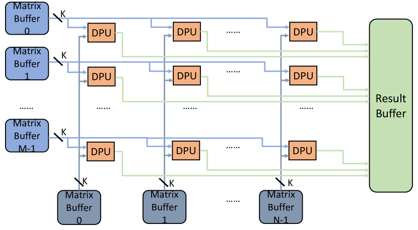
where is decomposed into weighted sum of the binary matrix multiplication. Such computation transform is hardware-friendly and can be efficiently implemented with LUT on FPGA, which is adopted in BISMO design (Umuroglu et al., 2018). Based on Eq. 1, BISMO propose a GEMM core (depicted in Figure 1 composed of a M-by-N DPU array, where each DPU unit performs the binary vector dot-product via the XNOR and pop-count. According to the bit-serial computing fashion, the computing latency of BISMO is proportional to the operand bit-width of and . Thus, such computing architecture is prone to compute with the low bit-width operands.
2.2. Model Quantization
DNN model quantization has emerged as a mandatory technique for high-performance DNN inference. Thanks to the advances in model quantization algorithm (Zhou et al., 2016; Choi et al., 2018; Choukroun et al., 2019; He et al., 2019; He and Fan, 2019; Liu et al., 2021), the activations and weights in 32-bit floating-point (fp32) can be quantized into extreme low bit-width with negligible inference accuracy degradation, using uniform (Jacob et al., 2018) or non-uniform quantizer (Miyashita et al., 2016) in quantization-aware training (He et al., 2019; He and Fan, 2019) or post-training quantization (Liu et al., 2021). In this work, we focus on the model quantization using -bit uniform quantizer, and its quantization function can be expressed as:
| (2) |
where is the step size. and are the upper and lower bound for the integer representation. is the clipping function, and denotes the round function. With the uniform quantizer adopted, two quantization schemes (uniform precision and mixed precision) are usually applied upon the entire DNN mode.
Uniform Precision. Uniform precision quantization assigns identical bit-width to each layer of target DNN. Researchers (Zhou et al., 2016; Choukroun et al., 2019; Gong et al., 2019) have shown that INT8, even INT4, can retain accuracy on many neural networks. For the general-purpose computing hardware (e.g., CPU or GPU), due to the hardware constraint, only INT4 and INT8 are supported. Thus, uniform precision quantization is a relatively general method, as most hardware platforms only support computation (e.g., MAC) in specific bit-width.
Mixed Precision. As the prior investigations (Cai et al., 2020; Wu et al., 2018; Wang et al., 2019) reveal the fact that layers of DNN own different redundancy, the quantization with varying bit-width on different layers emerges as a potential scheme to minimize the model size of target DNN. (Zhu et al., 2018) determines the layer-wise bit-width based on the entropy of weights and activations. (Dong et al., 2019) utilizes the second-order information, i.e., Hessian matrix, to determine the bit-width, where the block with higher top Hessian eigenvalue will be assigned with higher bit-width. Elthakeb et al. (Elthakeb et al., 2019) use the sample efficiency of Proximal Policy Optimization (PPO) to find the optimal bit-width, which is the first to use RL for quantization. Wang et al. (Wang et al., 2019) predict the layer-wise bit-width via Deep Deterministic Policy Gradient (DDPG) algorithm with the target hardware taken into consideration.
3. Architecture of N3H-Core
In this work, we propose a heterogeneous neural network accelerator called N3H-Core, which fully exploits both the DSP and LUT resources in a heterogeneous fashion. Its architecture, data flow and cost and latency models are specified as follows.
3.1. Architecture Overview of N3H-Core
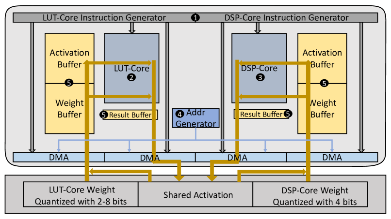
As depicted in Fig. 2, N3H-Core architecture consists of instruction generator, heterogeneous computing cores (i.e., LUT-core and DSP-core), address generator, peripheral buffers.
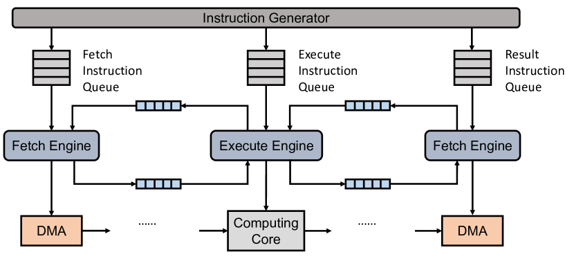
Instruction Generator. N3H-Core is an intra-layer asynchronous and inter-layer synchronous instruction-based neural network accelerator. Thus, the instructions adopted can be generally separated into two categories: operation instruction and synchronization instruction, which jointly work for accurate pipelining computation within LUT- and DSP- core. Within each layer, Operation Instructions are generated asynchronously and specifically for the LUT-Core and DSP-Core, consisting of three types {Fetch, Execute, Result} that corresponds to three operating phases of LUT- and DSP-core, respectively. 1) In Fetch phase, Direct-Memory Access (DMA) module loads weight and activation data from the off-chip DDR to on-chip buffers; 2) In Execute phase, data is transmitted from buffers to computing cores for multiplication and accumulation; 3) In Result phase, the calculation results from the LUT- and DSP-core are written back to the shared result buffer. Thanks to the synchronous instructions (Sync), two cores are synchronized after they complete the assigned workloads, then launch the computation of successive layer without conflicts.
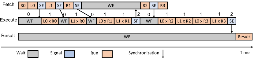
Based on prior designs (Umuroglu et al., 2018; Matam and Prasanna, 2013), we propose a new schedule for matrix multiplication and design Fetch, Execute and Result engines to run the corresponding instructions, as described in Fig. 3. Referring to Eq. 1, we assume the activation buffers possess the capacity of the activation matrix , and weight buffer is the half capacity of weight matrix . To begin with the first part111For simplicity, we write decomposed and in Eq. 1 as R0 and L0 respectively of and , R0 is fetched by fetch engine, then is fetched as well. Meanwhile, execute and fetch engines are in waiting status, i.e., Wait-Fetch (WF) and Wait-Execute (WE). When fetch instructions is completed, the fetch engine sends a synchronization signal to activate the execute engine, i.e., Sync-Execute (SE). After the execute engine receives the signal, it immediately transfer from WF status to run the execute instruction of L0R0. While the L0R0 is executing, the fetch engine start to load following binary matrix L1 for pipeling. After fetching the first tile of weight data R0 and R1, the weight buffer is filled, so the fetch engine is in WE status, waiting for a synchronization signal from execute engine. After the signal is received, the fetch engine continues to fetch the next tile of weight data R2 and R3. Once the R2 is fetched, the execute engine multiplies the pre-loaded binary matrices of in a sequence. When all the multiplications are done, the result engine receives the synchronization signal (Sync-Execute, SE) from the execute engine, then shift from Wait-Execute (WE) status to run Result instruction that store the computation result back to DDR. In this way, the design bridges the gap between data movement and processing.
For instruction compatibility for DSP- and LUT-core, all instructions are 128-bits composing different segments for information representation. For Fetch and Result instructions, they consist of base address (16-bits), stage control (3-bits), read /write range (1-bit) of on-chip buffer and base address (32-bits), offset (24-bits), and write/read range (16-bits) of the DDR. For Execute instruction, it includes the on-chip buffer data address, and the GEMM-Core parameters listed in Table 1. For sync instruction, it includes the current (1-bit) and next state (2-bits) of each Engine and the flag (3-bits) indicating the sent of synchronization token.
Heterogeneous Computing Core. To fully utilize the on-chip resource of a target FPGA for boosted computing power, we develop a heterogeneous computing core that consists of LUT-core and DSP-core. Given a computing task (e.g., inference with one layer of DNN), the computation workload is split w.r.t a designated ratio, then performed by the LUT- and DSP-core asynchronously. Note that, the optimization of workload split ratio will be discussed in Section 5.3. For the LUT-core, we adopt the open-sourced BISMO222BISMO: https://github.com/EECS-NTNU/bismo (Umuroglu et al., 2018) as its backbone, which is a GEMM kernel with run-time adjustable operand bit-width in virtue of the bit-serial computing mechanism. In contrast to the LUT-core operating in the bit-serial fashion, the DSP-core is developed for bit-parallel computing. Overall, the heterogeneous computing core incorporates prior-neglected rich LUT resources and introduces a more flexible weight-activation quantization scheme for accuracy lossless mapping.
Peripheral Buffer. To avoid the frequent off-chip memory access that hampers the overall inference latency and improve the throughput via pipelining, the proposed architecture allocates each computing core with input/weight/result buffers. Weight and activation data are fetched via Direct Memory Access (DMA) to the dedicated buffers, then transferred to the computing cores. Once the computation is done, the result stored in the result buffer is then written to DDR as the activation of the next layer.
Memory Control. Two workload partitions allocated to two computing cores are stored at different regions on DDR to make the data access more efficiently and avoid conflict. Address Generator controls the base address and strides to instruct two partitions fetched from DDR. After the computation of one layer is finished, gives new base addresses and strides to store the result.
| Notation | Description |
|---|---|
| Numbers of rows in LUT-Core (DPU array) | |
| Numbers of columns in LUT-Core (DPU array) | |
| Input bit width of DPU | |
| Depth of activation buffers in LUT-Core | |
| Depth of weight buffers in LUT-Core | |
| Numbers of rows in activation register array | |
| Numbers of columns in activation register array | |
| Numbers of columns in weight register array | |
| Depth of activation buffers in DSP-Core | |
| Depth of weight buffers in DSP-Core | |
| Bit-widths of quantized activation | |
| Bit-widths of quantized weight on LUT-Core | |
| Bit-widths of quantized weight on DSP-Core |
3.2. Heterogeneous Computing Core
3.2.1. LUT-Core
Through the conversion function (i.e., im2col), the computation of various parametric layers (e.g., convolution layer, fully-connected layers) can all be computed via the matrix multiplication (GEMM). Fig. 1 illustrates the architecture of LUT-Core. In LUT-Core, the buffers allocated to the row are designated as the activation buffer (indexed from to in Fig. 1), the activation buffers have the depth of , whose interface width is . Similarly, the buffer allocated to the column is weight buffers indexed from to , and the depth is , whose interface width is as well. Each DPU reads -bits from the activation buffers and -bits from weight buffers simultaneously, then store the binary dot multiplication results as partial sum. The LUT-Core can process bits in parallel. As listed in Table 1, are five important configuration parameters significantly affect the latency, which will be explored at design time.
3.2.2. DSP-Core
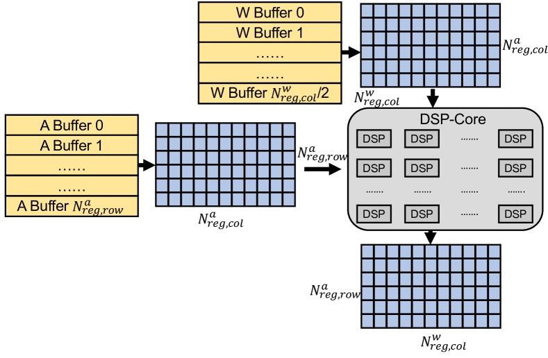
The architecture detail of DSP array is illustrated in Fig. 4. Note that, the DSP core performs the GEMM in tiling fashion as well. In Execute phase, a tile of input activation data and weight data are read from buffers into register arrays. The register array of activation data has rows and columns. Correspondingly, the register array of weight data has rows333Note that, the row size of weight register array is identical to the column size of activation register array. and columns. For activation buffer, the size of each row of activation register array is same as the activation buffer. Thus, the total bit-width of each buffer is , where is the activation bit-width. During the computing, each row of the activation array is filled with an activation buffer per cycle. For weight buffer, the bit-width of each buffer is , and each two columns of the weight register array is filled with a weight buffer, thus it requires two cycles to fill the weight register array with weight buffer.
3.3. Cost and Latency Model
To minimize the latency by finding the optimal architecture configuration, we build the cost and latency models here for rapid design space exploration. The cost model simulates the resource utilization of LUT, BRAM, and DSP on FPGA, while the architecture configuration in Table 1 is constrained by available on-chip resource. Besides, the latency model describes the end-to-end inference latency.
DSP-Core Cost Model. As described in Section 3.2.2, the number of activation buffer equals to the , and each buffer has the depth of with the interface of . Since our DSP-core is designed for 4-bit multiplication, the quantized activation bit-width ranges from 2 to 4 bits. When the activation bit-width is less than 4, we pad zeros to make it 4-bits for storing in buffers. The BRAMs forming buffers are 1024 in-depth and 36-bits wide, and we use the 32-bits for convenience. Thus, the BRAM size consumed by DSP-Core is formulated as:
| (3) |
where is the BRAM size that one activation buffer consumes, and is the size of activation buffers. Likewise, since we allocate data in one buffer to two columns of the weight register array, the amount of weight buffers is , and is the BRAM size that one weight buffer consumed. For LUT usage of DSP-Core, it is mainly consumed by the instruction generator and the control module, which is about 1000 as a constant (). The utilization rate of DSP resources is predefined as 100% at design time. The DSP-Core utilizes all the DSP resource available on chip, which means .
LUT-Core Cost Model. Since we adopt the BISMO (Umuroglu et al., 2018) as the backbone of LUT-core, we inherits its cost model as:
| (4) |
| (5) |
where are the fitting coefficient. From Eq. 4, the LUT utilization is proportional to , , and . We use 1024 in-depth and 36-bits wide BRAMs to build the buffer, and we only use 32-bits of the original interface. As mentioned before, there are activation buffers and each of them is comprised of BRAMs. Similarly, the BRAMs consumed by weight buffer is calculated by Eq. 5.
DSP-Core Latency Model. As the DSP-core is an instruction-oriented computing unit whose instruction pipeline is organized in a specific pattern, we build its latency model w.r.t its instruction pipeline. We focus on the execute engine and count the latency as following queues: , , and . These four parts of latency is relevant to the parameters {, , , , } in Table 1. Then, we trace the instructions streams and accumulate the latency of each phase on execute engine. Note that, is the latency of waiting for fetching data (i.e., phases denoted by 0 in Fig. 3), is the latency of execution (phases denoted by 1), is the latency of sending signal (indicated by 2), and is the latency of result phase. By accumulating each latency, the computational latency of one layer is formulated as:
| (6) |
To fully utilize the DSP resource on-chip, we adopt a simple simulation method that , are fixed to 16, and only can be modified that determines the latency performance. Therefore, it ensures that DSPs are fully-utilized by modifying only one parameter, and a simple core design method is provided at the same time. Then, the calculation of Eq. 6 can be simplified as:
| (7) |
LUT-Core Latency Model. Likewise, the latency model of LUT-Core is built in the same manner via describing and simulating the instruction streams. However, the main difference is that LUT-Core computes the MACs in a bit-serial fashion, whose latency is determined by the bit-width of activation () and weight () matrices. Thus, the parameters that relevant to the LUT-Core latency is {, , , , , , }, and the latency model of LUT-Core is formulated as:
| (8) |
Note that, the weight buffer reads one tile at once. Thus, the capacity of the weight buffer is the size of one tile weight data, while the depth change will not affect the latency. Correspondingly, we simplify the latency model of LUT-Core as:
| (9) |
where such simplification also shrink the design space to be explored by reducing the variation of .
As N3H-Core performs the DNN inference in a layer-wise synchronization manner, the total computation latency of target DNN with -layers can be expressed as:
| (10) |
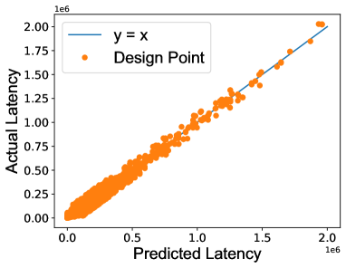
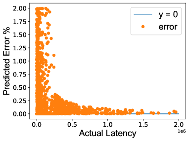
where the and denotes the computation latency taken by the LUT-core and DSP-core to complete the assigned workload for -th layer respectively. Since the instructions of our LUT-core and DSP-core are scheduled in static pipeline, the latency model formulated via accumulated execution time of schedule instruction is relatively accurate. To verify our latency model, we test 10000 design points with design knobs listed on Table 1 of original manuscript using randomly generated value, where the result is shown in Fig. 5 with prediction error less than 2%.
4. Hybrid Quantization with Mixed Precision
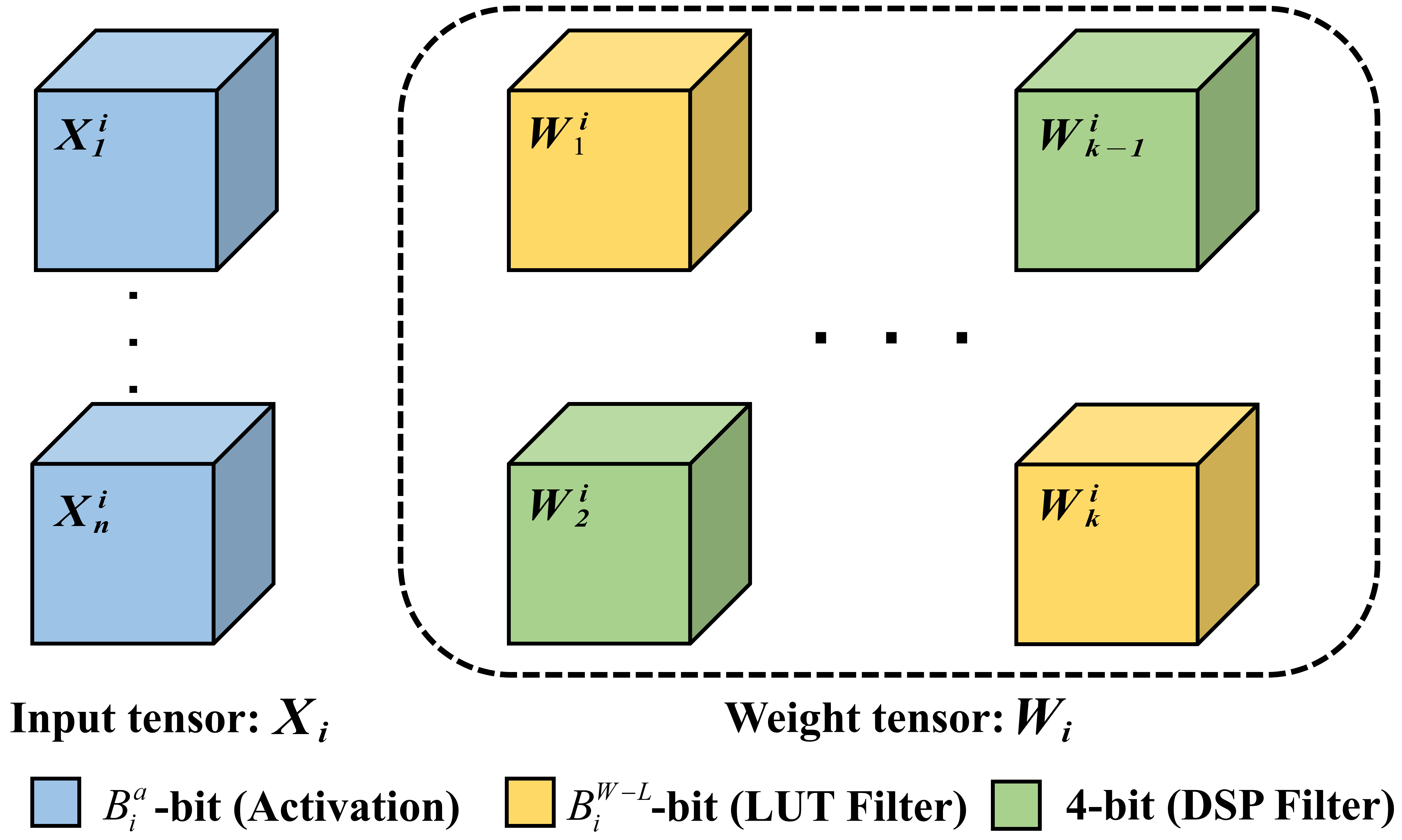
Suppose an -layer DNN as and denotes the -th layer weight and input/activation tensor respectively, where is the kernel size444 for fully-connected layer, and are number of input and output channels. The weight tensor can be viewed as a set , where denotes the -th filter. Our work applies filter-wise quantization, which takes a finer-grained strategy with as its granularity. For different filters in one layer, 3-D tensor is assigned with different quantization bit-width.
The hybrid quantization method integrates both uniform- and mixed-precision quantization in this work. The computation of one layer for DSP- and LUT-core is allocated in the granularity of filters. All the computations conducted by DSP-core are 4-bits quantized on weights. The rest of filters computed by LUT-core are quantized with bits (-bits) which is determined by our optimization framework (Section 5). Note that, varies in different layers. The filter allocation ratio will be discussed in Section 5.3, which determines the number of filters allocated to DSP-/LUT-core on each layer. Besides, we need to consider which filters should be allocated to DSP-/LUT-core. In this work, the filter allocation (to DSP/LUT) depends on the KL-divergence of the original filter weight distribution and its quantized weight distribution (calibrated via one batch of images). The filters with greater in one layer will be allocated to the computing core with higher bit-width, since the quantization bit-widths of LUT filters is flexible. Now, the filter number and type allocation problems are settled.
We adopt the layer-wise quantization manner for activations shared by both LUT- and DSP-core. The activation and weight of first and last layer are quantized into 8-bits. In our work, we set the activation bit-widths range as 2-4 bits for all other layers, as the LUT-core enjoys much less latency with operands in low bit-width. Moreover, we linearly quantize the weights and activations of each layer using -bits and -bits respectively. The linearly quantized model only requires fixed-point computing unit, which is more efficient in our heterogeneous architecture. The proposed quantization method of the convolution layer is depicted in Fig. 6.
5. Framework for Optimized System
5.1. Framework Overview
This section describes our framework to automatically generate the optimized system configuration for N3H-Core to achieve the optimized performance across varying DNNs and FPGAs. The objects to be optimized by the framework come in threefold: 1) Resource Allocation. The framework configures the design parameters listed in Table 1 to achieve the optimized resource allocation for both LUT-core and DSP-core; 2) Workload Split. As the N3H-Core splits the computing task into LUT- and DSP-core in the layer-wise fashion, the framework is expected to split the computation task for workload balance properly; 3) Quantization bit-width. Since LUT-core supports operands with flexible bit-width while DSP-core only supports the fixed one (int4 in this work), the quantization bit-width affects the overall inference latency and accuracy.
5.2. Resource allocation & Quantization
As discussed in Section 3, we formulate the latency model for LUT- and DSP-core, and design factors influencing the latency and the corresponding ranges are tabulated in Table 2. Design factors are related to the resource allocation. The left design factors are the quantization bit-widths of LUT filters and activations of each DNN layer. We leverage the Reinforcement Learning (RL) with DDPG algorithm (Qiu et al., 2019) for the design space exploration (can be viewed as sequential decision making) to identify the optimal system configuration with low latency but high accuracy. The change of design factors leads to different resource usage estimated by our cost model, which is constrained by the available resources on the target FPGA devices.
| Design Factors | Range on DA | Range on DB |
|---|---|---|
| 1-50 | 1-252 | |
| 1-50 | 1-252 | |
| 2-8 | 2-8 | |
| 2-4 | 2-4 |
5.3. Neuron-based workload split
For each layer, the filter-based workload split ratio is defined as:
| (11) |
Where is the number of neurons/filters and is the number of filters computed by LUT-core. After the quantization bit-widths of the -th layer are determined by the agent, the best workload split ratio is computed by minimizing the latency of the -th layer, as defined:
| (12) |
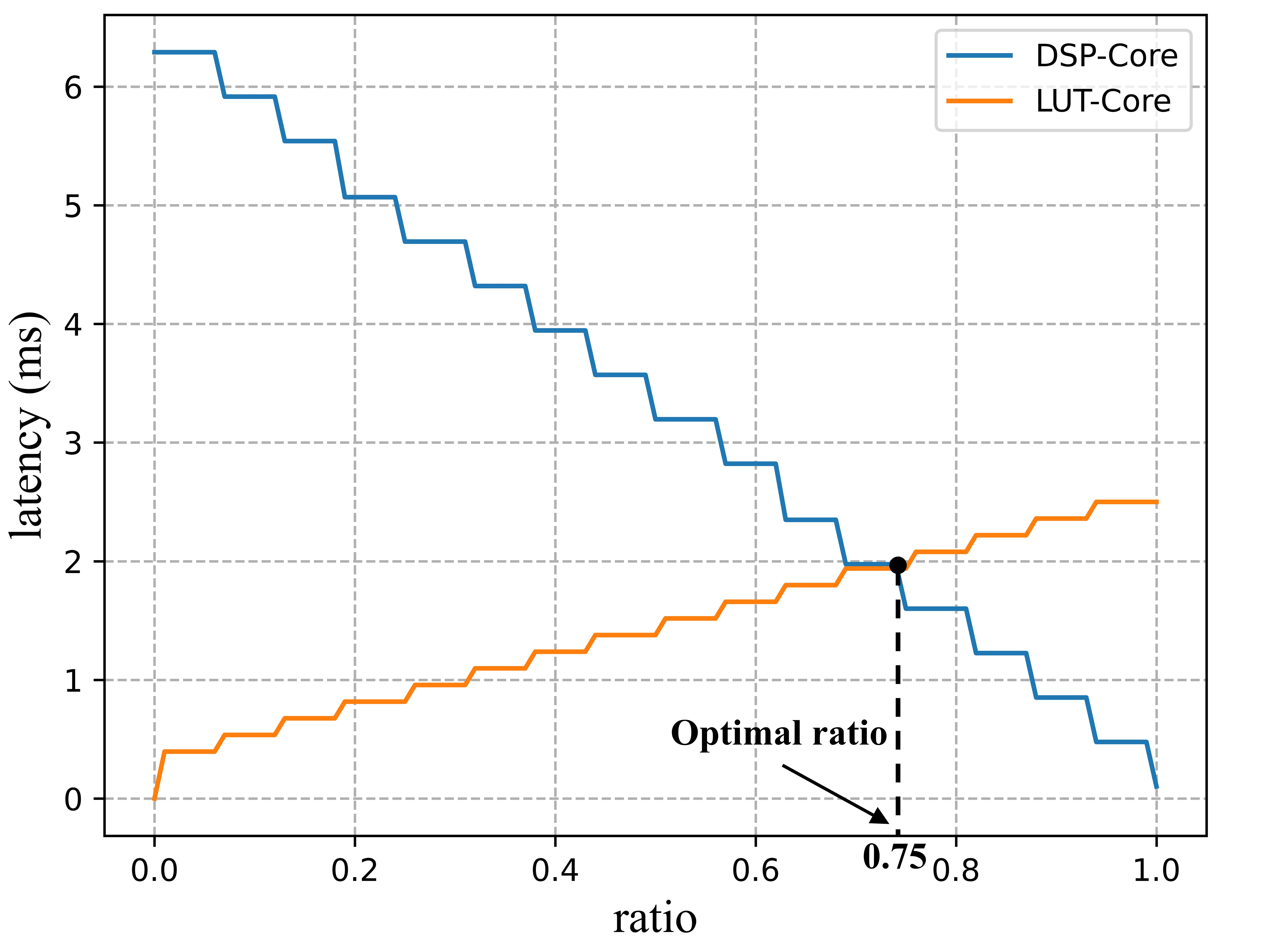
The generated ratio is the optimal filter allocation strategy for inter-layer parallelism of N3H-Core. Fig. 7 shows an example of the relationship between the latency and ratio. From the figure, the optimized ratio is 0.75, which means filters are computed by the LUT-core and the rest filters are assigned to DSP-core.
5.4. RL implementation details
The overview of our DDPG based RL learning framework (He et al., 2018) to explore the both the architecture configuration and workload assignment between heterogeneous cores is depicted in Fig. 8. Details of action space, state space, reward and etc are given as follows.
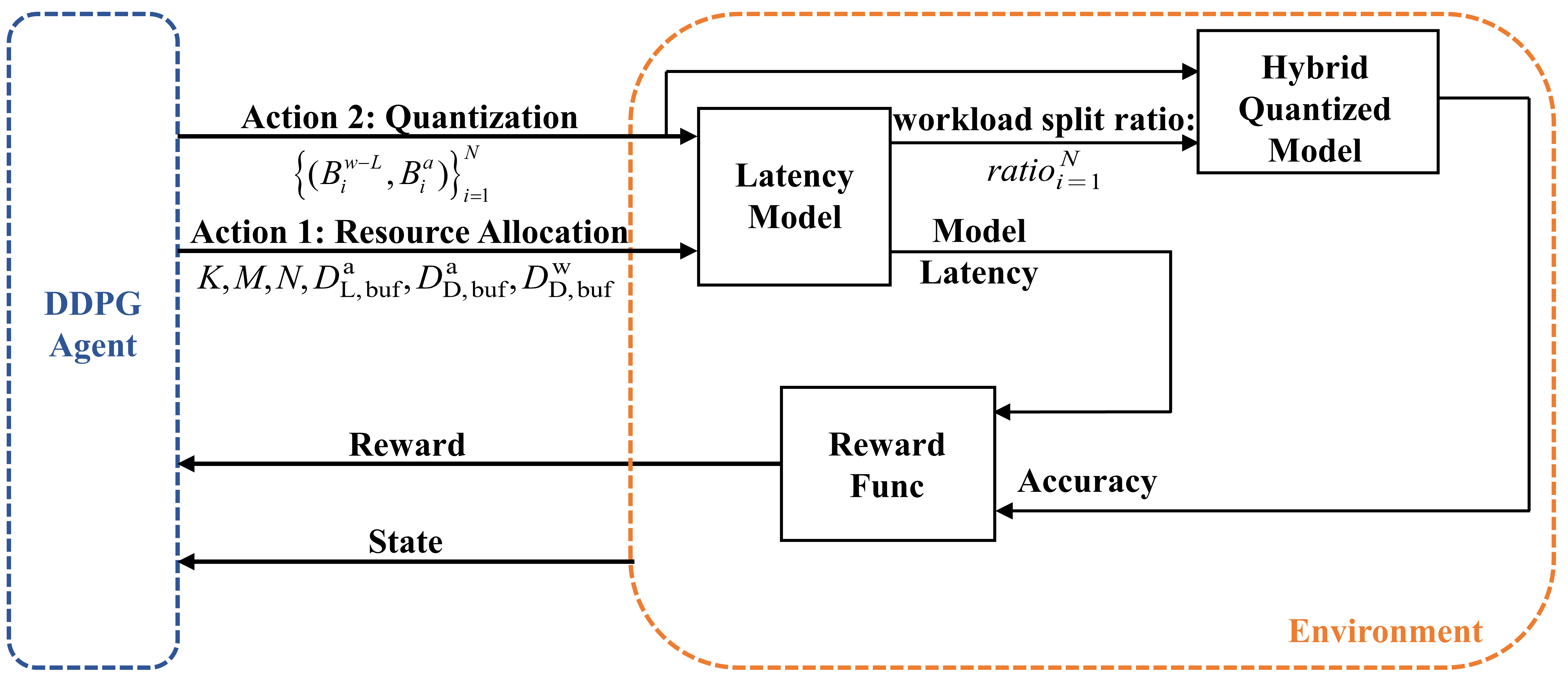
5.4.1. Action Space.
The action space contains two tasks of actions: action-1 and action-2 in sequence. The action-1 decides the resource utilization design factors which is constrained by the available resources of given FPGA devices. Table 2 provides the range of resource utilization design factors on two FPGAs. In each episode, the RL agent takes 6+2N action steps, where N is the number of layers of given DNN.
For action-1, the agent chooses the hardware-related factors sequentially at the first 6 time steps. For each time-step, the agent output one action applies on one aforementioned hardware factor, which can be described as:
| (13) |
where . The continuous action (range: [0, 1]) of the DDPG agent are discretized by round function into the range of 6 design factors in integer. Note that, ,, , are in the format of where is a constant parameter and is a variable. For these 4 parameters, is the range of the parameter , so the actions will be multiplied with their corresponding constant parameters which are shown in Table 2.
For action-2, the agent chooses the software-related factors with 2N steps. The actions can be denoted as:
| (14) |
where is the bit-width range in Table 2.
5.4.2. State Space
The state space for the -th time step is expressed as:
| (15) |
where is the binary indicator for the current task (0 for , 1 for ) , is the layer index, is the DNN information of the -th layer, is the calculated filter number allocation ratio in the -th layer, is the action of the current time step. , and are set as 0 when =0. The DNN information of the -th layer is a group of parameters defined as:
| (16) |
where and are #input/output channels, and are the sizes of the kernel, stride and feature map. denotes #parameters. is the binary index for shortcut layers of ResNet (He et al., 2016) and depthwise layers of MobileNet (Sandler et al., 2018). If shortcut or depthwise, it is set 1, otherwise 0. is the binary index for the type of the current action: 0 for quantization of LUT filters , 1 for quantization of activations .
Thus, the entire state space can be unfolded as:
| (17) |
In addition, we normalize each dimension of the state space into [0, 1] to make them in the same scale.
5.4.3. Reward.
After actions are taken in each episode, the model latency with current design configuration is estimated by our latency model, and the DNN is quantized w.r.t the identified quantization scheme. Then, we retrain the quantized model for one epoch to recover the accuracy, denoted as . The reward function is designed by combining the model latency and accuracy , which is formulated as:
| (18) |
where is the latency bound or target latency, is the baseline accuracy of our model, is a scaling factor. Note that, the reward remains less than -1 when the model latency exceeds the latency bound, otherwise the reward is in the interval of (-1, 1).
6. Experiments
In this section, we conduct experiments on various representative DNNs and FPGA devices to demonstrate the merits of hardware and software parts of N3H-Core.
6.1. Experimental Setup
Networks and Dataset. In this work, we uses two the classic image classification neural architectures, i.e., ResNet-18 (He et al., 2016) and MobileNet-V2 (Sandler et al., 2018) with large-scale ImageNet dataset (Deng et al., 2009). The data augmentation is identical as stated in (He et al., 2016). The full-precision pretrained model utilized in the N3H-Core is obtained from the Pytorch model hub (Paszke et al., 2017). Hyper-parameters of software framework. The RL agent explores 900 episodes for each experiment setting. For each episode, if the model latency is within the latency bound, we will retrain the quantized model for one epoch to recover its accuracy for reward evaluation. We use SGD as optimizer with a fixed learning rate of 0.001 and momentum of 0.9. We randomly sample 100 categories of ImageNet to accelerate the exploration process. FPGA platforms. Two FPGA boards, i.e., XC7Z020 and XC7Z045, are chosen as the target hardware platforms. With the N3H-Core architecture deployed upon different FPGAs, the device-specific configuration scheme is given by the framework automatically, constrained by the available hardware resources (e.g., DSP, LUT and BRAM). The operating frequency is set to 100MHz.
| Configuration | K | M | N | |||
|---|---|---|---|---|---|---|
| DANResNetT30ms | 128 | 7 | 17 | 1024 | 10242 | 1024 |
| DANResNetT35ms | 128 | 8 | 16 | 1024 | 10242 | 1024 |
| DANMobileNetT5ms | 64 | 18 | 12 | 1024 | 102411 | 1024 |
| DANMobileNetT7ms | 64 | 26 | 8 | 1024 | 10249 | 1024 |
| DBNResNetT25ms | 512 | 11 | 17 | 1024 | 10246 | 10242 |
| DBNResNetT30ms | 512 | 14 | 14 | 1024 | 102415 | 1024 |
| DBNMobileNetT5ms | 64 | 35 | 22 | 1024 | 102419 | 102411 |
| DBNMobileNetT6ms | 64 | 44 | 18 | 1024 | 102420 | 10248 |
6.2. Results and Analysis
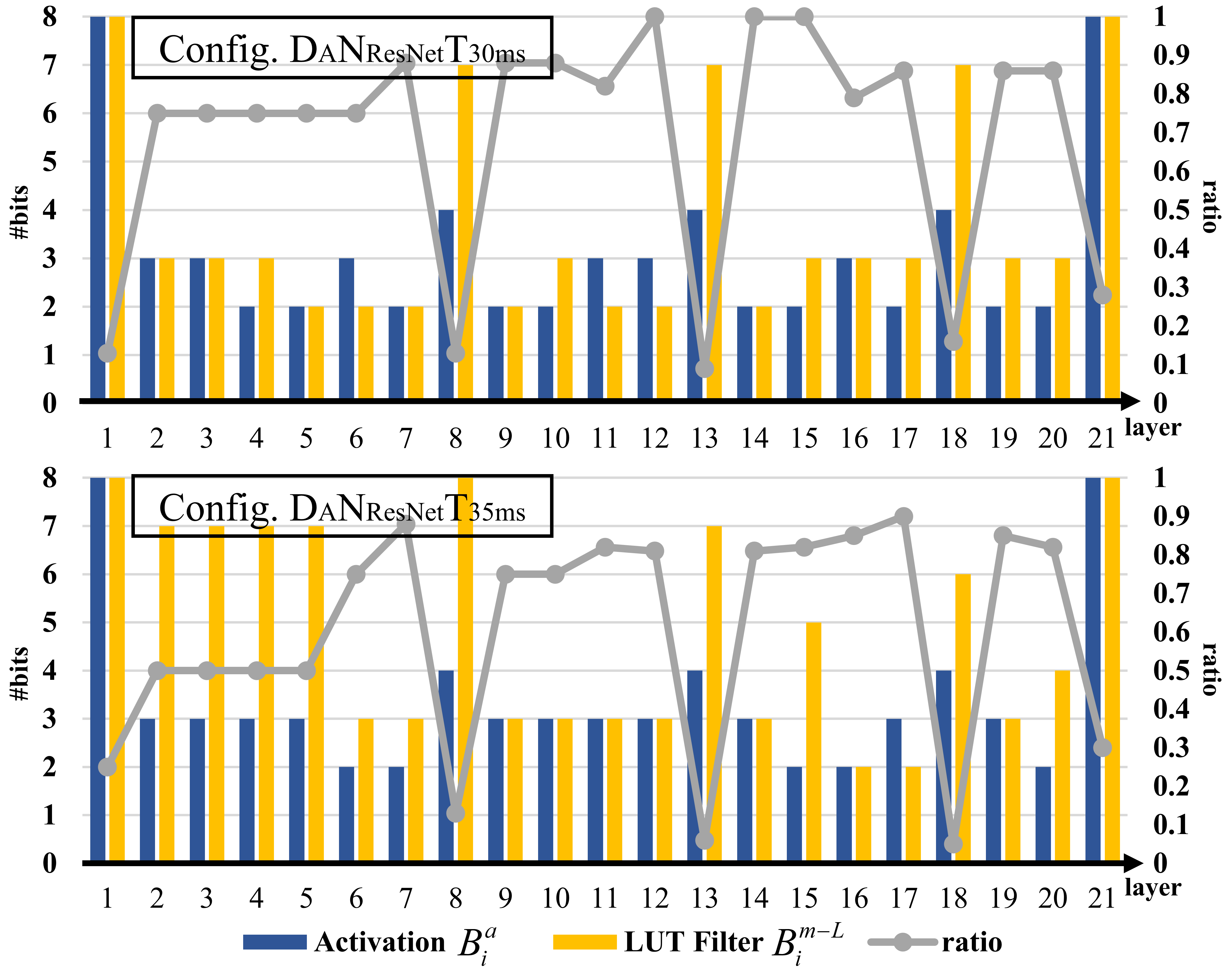
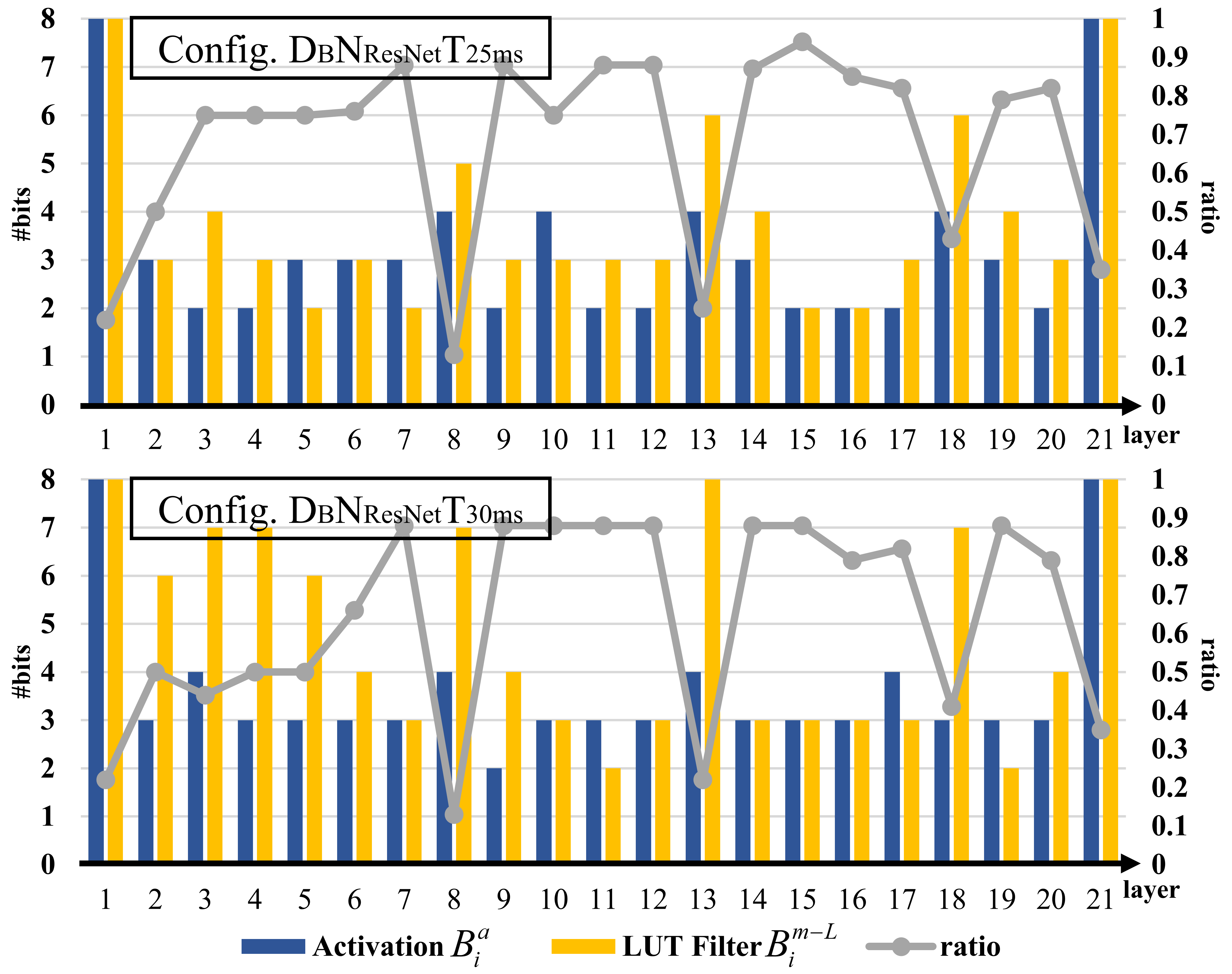
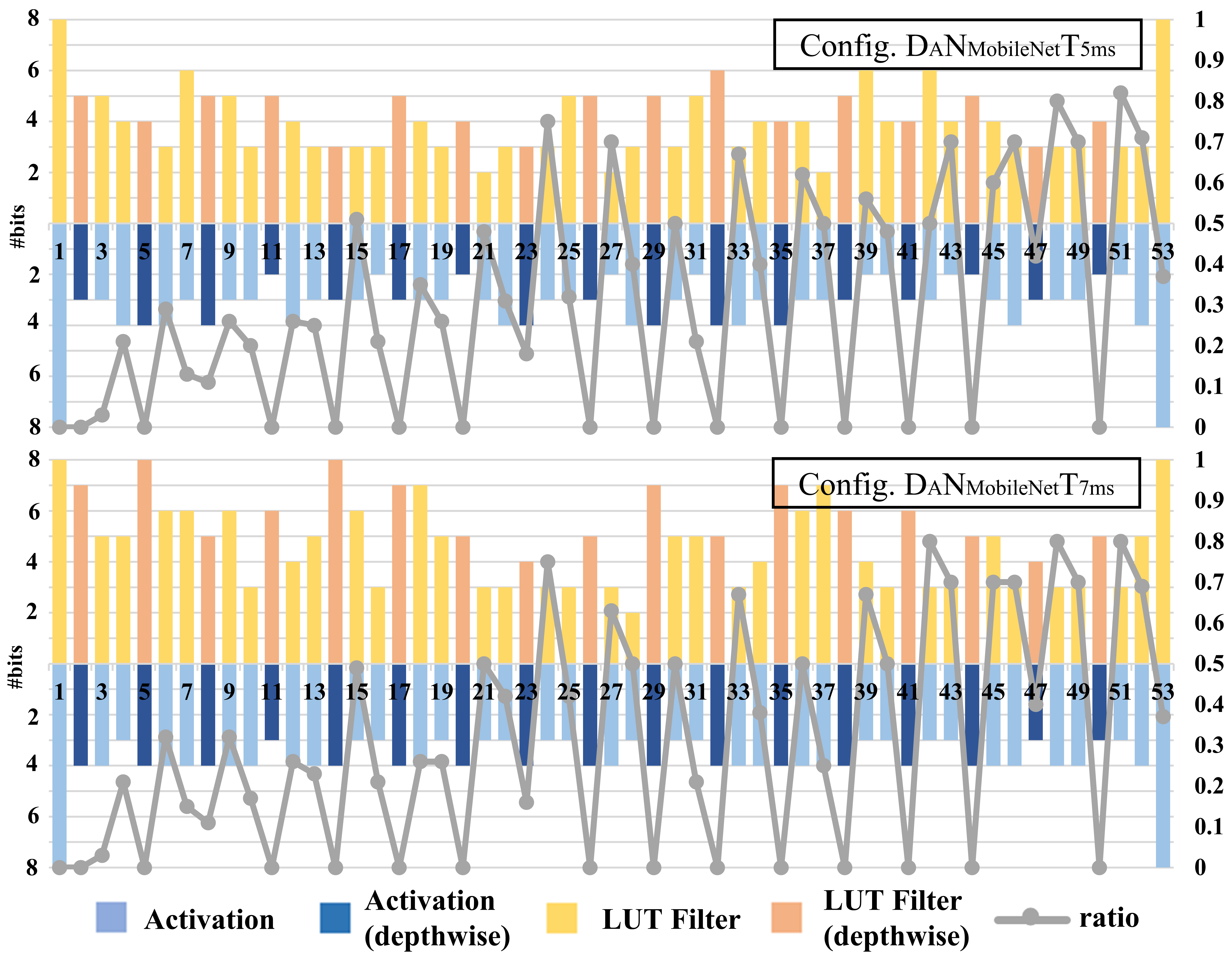
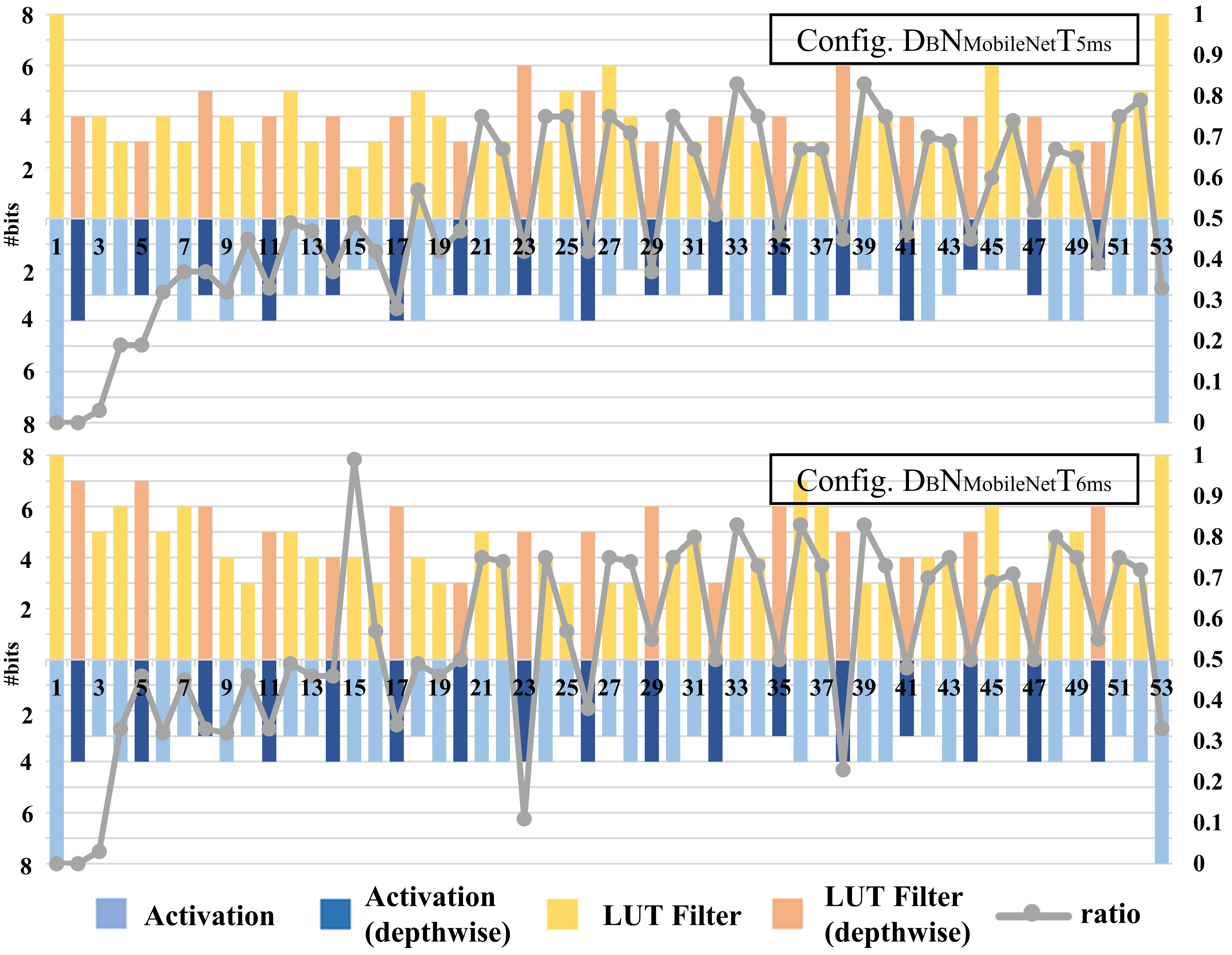
We evaluate the framework under different target latency bounds, and generate 8 configuration combinations for the two DNNs and two FPGAs. The accuracy and latency of each configuration are tabulated in Table 5, where the configuration details are given in Table 3. For each configuration, we also provide the quantization bit-widths and the workload-split ratio of each layer in Figs. 9, 10, 11 and 12.
[b] Implementation MobileNet-V2 (Wu et al., 2019) ResNet-18 (Chang et al., 2021) MobileNet-V2 (Chang et al., 2021) ResNet-18 Ours1 MobileNet-V2 Ours2 Device ZU2EG ZU9EG XC7Z020 XC7Z045 XC7Z020 XC7Z045 XC7Z020 XC7Z045 XC7Z020 XC7Z045 Bit-width (W/A) 8/8 4/4 4/4 Flexible Flexible Flexible Flexible Top-1 Accuracy (%) 68.1 70.27 65.64 70.45 70.39 66.25 66.04 Frequency (MHz) 430 333 100 100 100 100 LUT 31198 161944 28288 145049 28288 145049 39623 152868 45765 192624 DSP 212 2070 220 900 220 900 220 900 220 900 BRAM 145 771 56 225.5 56 225.5 137 541 137 461 Latency (ms) - - 47.10 40.36 8.29 7.28 35.79 32.47 7.51 6.62 Throughput (GOPS) - - 77.0 359.2 71.8 326.9 101.3 446.8 80.1 363.5 Frame Rate (FPS) 205.3 809.8 21.3 99.1 120.7 549.3 27.9 123.2 133.2 604.2 GOPS/DSP - - 0.350 0.391 0.326 0.363 0.460 0.496 0.364 0.404 GOPS/kLUT - - 2.725 2.475 2.538 2.252 2.557 2.923 1.750 1.887
-
1
Config. DANResNetT35ms & Config. DBNResNetT30ms
-
2
Config. DANMobileNetT7ms & Config. DBNMobileNetT6ms
|
|
|
|
|
||||||||||
|---|---|---|---|---|---|---|---|---|---|---|---|---|---|---|
| ResNet-18 | ||||||||||||||
| Pretrained Baseline | 32/32 | 69.76/89.08 | N/A | N/A | ||||||||||
| Manual Config. DANResNet | 4/4 | 69.65/89.11 | 40.96 | 42.26 | ||||||||||
| Auto. Config. DANResNetT30ms | Flexible | 67.28/87.85 | 29.14 | 31.43 | ||||||||||
| Auto. Config. DANResNetT35ms | Flexible | 70.45/89.54 | 34.95 | 35.79 | ||||||||||
| Manual Config. DBNResNet | 4/4 | 69.65/89.11 | 30.26 | 32.77 | ||||||||||
| Auto. Config. DBNResNetT25ms | Flexible | 66.81/87.19 | 24.83 | 26.90 | ||||||||||
| Auto. Config. DBNResNetT30ms | Flexible | 70.39/89.33 | 29.52 | 32.47 | ||||||||||
| MobileNet-V2 | ||||||||||||||
| Pretrained Baseline | 32/32 | 71.88/90.29 | N/A | N/A | ||||||||||
| Mannual Config. DANMobileNet | 4/4 | 65.18/75.77 | 8.85 | 9.15 | ||||||||||
| Auto. Config. DANMobileNetT5ms | Flexible | 62.76/73.32 | 4.93 | 5.66 | ||||||||||
| Auto. Config. DANMobileNetT7ms | Flexible | 66.25/76.09 | 6.95 | 7.51 | ||||||||||
| Auto. Config. DBNMobileNetT5ms | Flexible | 63.41/73.56 | 4.86 | 5.33 | ||||||||||
| Auto. Config. DBNMobileNetT6ms | Flexible | 66.04/75.88 | 5.93 | 6.62 | ||||||||||
6.2.1. Resource allocation Analysis
From Table 3, on DA we can find that is greater when the DNN is ResNet-18. denotes the computational parallelism of input channels of activation. A large allows more input channels to be computed in parallel, improving the computation efficiency. Compared with ResNet, MobileNet contains depth-wise layers which occupy one-third of the number of layers. Since depth-wise layers has a small number of input channels, the agent tends to assign a small to LUT-Core. It indicate that LUT-Core is more efficient in computing ResNet than MobileNet. Thus, for MobileNet, the agent allocates more BRAMs to DSP-Core, which allows DSP-Core compute faster to compensate for the inefficiency of LUT-Core. As shown in Fig. 11, for the same reason, the split ratios of many depthwise layers in MobileNet are zero, which means that the workload of the depthwise layer is solely assigned to the DSP-Core for minimized latency.
6.2.2. Quantization Analysis
In Fig. 9, it reveals that the RL agent assigns more bit-width in down-sampling layers (layer 8, 13, 18). To avoid the information bottleneck, higher bit-width are assigned to those layers (e.g., 7-bits for LUT-Core filters and 4-bits for shared activations). When the target latency bound is set to 30ms, the quantization bit-width becomes lower under the strict limitation. Consequently, the LUT-Core latency is reduced, and more workload is assigned to the LUT-Core to keep the latency below the bound. This proves that the agent can automatically analyze the latency and adjust the bit-width and ratio. As shown in Fig. 11, LUT-Core is not efficient to compute depth-wise layers, thus the workload split ratio of depth-wise layers is lower than point-wise layers. When the bound is set to 5ms, the bit-width across layers is further lowered compared to the 7ms counterpart. On DB, the configuration of quantization and ratio shows the same trend.
6.2.3. Comparison with the state-of-arts accelerators
We selected the results of ResNet18 and MobileNet networks on two devices XC7Z020 and XC7Z045, as shown in Table 4, and compare the experimental results with the existing state-of-arts designs. When deploying ResNet18 on the given two FPGA devices, we obtain comparable accuracy while reducing latency by and compared to the Mix&Match design (Chang et al., 2021). The Mix&Match is also a heterogeneous architecture utilizing DSP and LUT resources, but without exploring the design space, our latency-centric architecture outperforms it on resource utilization, quantization bit-width flexibility, and performance (e.g., latency, throughput and frame rate), even though they adopt more hardware-friendly power-of-2 (Liu et al., 2021) quantization scheme.
As can be found in Table 4, our proposed optimization framework makes better utilization of the on-chip resources, consuming more BRAMs and LUTs to boost the performance. In terms of the throughput per resource unit, the GOPS/DSP is higher on both devices. The GOPS/kLUT on XC7Z020 is less, but when more batches are computed simultaneously on XC7Z045, it outperforms the design in (Chang et al., 2021). On MobileNet, we get the speedup by about on both FPGA devices. The lower performance improvement on MobileNet over ResNet is due to the low computation efficiency of LUT-Core on MobileNet. This is also reflected in the efficiency of hardware resource usage. Despite the performance improvement, the throughput per resource unit on both devices is lower than Mix&Match (Chang et al., 2021). Therefore, the proposed heterogeneous architecture has a limited effect on depth-wise acceleration. Moreover, in terms of the frame-rate (FPS), our design outperforms the mix&match, and will outperforms design in (Wu et al., 2019) ( FPS) as well when it operates at 100MHz.
7. Conclusion
In this paper, we propose a heterogeneous architecture on FPGA with two cores (DSP/LUT-core) computing synchronously for efficient DNN inference. We also propose a hybrid quantization scheme which quantizes the NN weights according to the filter computation allocation. To rapid hardware-mapping evaluation and find the optimal resource allocation (BRAM, LUT) scheme for DSP- and LUT-core, we build the latency and cost models for both that parameterized by architecture configuration knobs. Based on aforementioned models, we utilize the reinforcement learning agent to identify the optimal design considering both resource allocation and quantization in an end-to-end fashion, for low latency and high accuracy. The framework can adapt to different FPGAs by changing the available resources in the cost model. We utilize two FPGAs XC7Z020 and XC7Z045 as the test-beds to evaluate our framework, and the explored configuration can reduce latency by 1.12-1.32 compared with the state-of-the-art Mix&Match design.
Acknowledgements.
This work was supported by Alibaba Group through Alibaba Innovative Research Program and National Natural Science Foundation of China (Grant No. 62102257).References
- (1)
- Brown et al. (2020) Tom B Brown, Benjamin Mann, Nick Ryder, Melanie Subbiah, Jared Kaplan, Prafulla Dhariwal, Arvind Neelakantan, Pranav Shyam, Girish Sastry, Amanda Askell, et al. 2020. Language models are few-shot learners. arXiv preprint arXiv:2005.14165 (2020).
- Cai et al. (2020) Yaohui Cai, Zhewei Yao, Zhen Dong, Amir Gholami, Michael W Mahoney, and Kurt Keutzer. 2020. Zeroq: A novel zero shot quantization framework. In Proceedings of the IEEE/CVF Conference on Computer Vision and Pattern Recognition. 13169–13178.
- Chang et al. (2021) Sung-En Chang, Yanyu Li, Mengshu Sun, Runbin Shi, Hayden K.-H. So, Xuehai Qian, Yanzhi Wang, and Xue Lin. 2021. Mix and Match: A Novel FPGA-Centric Deep Neural Network Quantization Framework. In 2021 IEEE International Symposium on High-Performance Computer Architecture (HPCA). 208–220. https://doi.org/10.1109/HPCA51647.2021.00027
- Chen et al. (2016) Yu-Hsin Chen, Tushar Krishna, Joel S Emer, and Vivienne Sze. 2016. Eyeriss: An energy-efficient reconfigurable accelerator for deep convolutional neural networks. IEEE journal of solid-state circuits 52, 1 (2016), 127–138.
- Chen et al. (2019) Yu-Hsin Chen, Tien-Ju Yang, Joel Emer, and Vivienne Sze. 2019. Eyeriss v2: A flexible accelerator for emerging deep neural networks on mobile devices. IEEE Journal on Emerging and Selected Topics in Circuits and Systems 9, 2 (2019), 292–308.
- Choi et al. (2018) Jungwook Choi, Zhuo Wang, Swagath Venkataramani, Pierce I-Jen Chuang, Vijayalakshmi Srinivasan, and Kailash Gopalakrishnan. 2018. Pact: Parameterized clipping activation for quantized neural networks. arXiv preprint arXiv:1805.06085 (2018).
- Choukroun et al. (2019) Yoni Choukroun, Eli Kravchik, Fan Yang, and Pavel Kisilev. 2019. Low-bit Quantization of Neural Networks for Efficient Inference.. In ICCV Workshops. 3009–3018.
- Deng et al. (2009) Jia Deng, Wei Dong, Richard Socher, Li-Jia Li, Kai Li, and Li Fei-Fei. 2009. Imagenet: A large-scale hierarchical image database. In 2009 IEEE conference on computer vision and pattern recognition. Ieee, 248–255.
- Dong et al. (2019) Zhen Dong, Zhewei Yao, Amir Gholami, Michael W Mahoney, and Kurt Keutzer. 2019. Hawq: Hessian aware quantization of neural networks with mixed-precision. In Proceedings of the IEEE/CVF International Conference on Computer Vision. 293–302.
- Elthakeb et al. (2019) Ahmed Elthakeb, Prannoy Pilligundla, FatemehSadat Mireshghallah, Amir Yazdanbakhsh, Sicuan Gao, and Hadi Esmaeilzadeh. 2019. Releq: An automatic reinforcement learning approach for deep quantization of neural networks. In NeurIPS ML for Systems workshop, 2018.
- Esser et al. (2019) Steven K Esser, Jeffrey L McKinstry, Deepika Bablani, Rathinakumar Appuswamy, and Dharmendra S Modha. 2019. Learned step size quantization. ICLR (2019).
- Fedus et al. (2021) William Fedus, Barret Zoph, and Noam Shazeer. 2021. Switch Transformers: Scaling to Trillion Parameter Models with Simple and Efficient Sparsity. arXiv preprint arXiv:2101.03961 (2021).
- Gong et al. (2019) Ruihao Gong, Xianglong Liu, Shenghu Jiang, Tianxiang Li, Peng Hu, Jiazhen Lin, Fengwei Yu, and Junjie Yan. 2019. Differentiable soft quantization: Bridging full-precision and low-bit neural networks. In Proceedings of the IEEE/CVF International Conference on Computer Vision. 4852–4861.
- Goodfellow et al. (2016) Ian Goodfellow, Yoshua Bengio, Aaron Courville, and Yoshua Bengio. 2016. Deep learning. Vol. 1. MIT press Cambridge.
- Guo et al. (2017) Kaiyuan Guo, Lingzhi Sui, Jiantao Qiu, Jincheng Yu, Junbin Wang, Song Yao, Song Han, Yu Wang, and Huazhong Yang. 2017. Angel-eye: A complete design flow for mapping cnn onto embedded fpga. IEEE Transactions on Computer-Aided Design of Integrated Circuits and Systems 37, 1 (2017), 35–47.
- He et al. (2016) Kaiming He, Xiangyu Zhang, Shaoqing Ren, and Jian Sun. 2016. Deep residual learning for image recognition. In Proceedings of the IEEE conference on computer vision and pattern recognition. 770–778.
- He et al. (2018) Yihui He, Ji Lin, Zhijian Liu, Hanrui Wang, Li-Jia Li, and Song Han. 2018. Amc: Automl for model compression and acceleration on mobile devices. In Proceedings of the European conference on computer vision (ECCV). 784–800.
- He and Fan (2019) Zhezhi He and Deliang Fan. 2019. Simultaneously optimizing weight and quantizer of ternary neural network using truncated gaussian approximation. In Proceedings of the IEEE/CVF Conference on Computer Vision and Pattern Recognition. 11438–11446.
- He et al. (2019) Zhezhi He, Boqing Gong, and Deliang Fan. 2019. Optimize deep convolutional neural network with ternarized weights and high accuracy. In 2019 IEEE Winter Conference on Applications of Computer Vision (WACV). IEEE, 913–921.
- Jacob et al. (2018) Benoit Jacob, Skirmantas Kligys, Bo Chen, Menglong Zhu, Matthew Tang, Andrew Howard, Hartwig Adam, and Dmitry Kalenichenko. 2018. Quantization and training of neural networks for efficient integer-arithmetic-only inference. In Proceedings of the IEEE Conference on Computer Vision and Pattern Recognition. 2704–2713.
- Liu et al. (2021) Fangxin Liu, Wenbo Zhao, Zhezhi He, Yanzhi Wang, Zongwu Wang, Changzhi Dai, Xiaoyao Liang, and Li Jiang. 2021. Improving Neural Network Efficiency via Post-Training Quantization With Adaptive Floating-Point. In Proceedings of the IEEE/CVF International Conference on Computer Vision. 5281–5290.
- Matam and Prasanna (2013) Kiran Kumar Matam and Viktor K. Prasanna. 2013. Energy-efficient large-scale matrix multiplication on FPGAs. 2013 International Conference on Reconfigurable Computing and FPGAs, ReConFig 2013 (2013). https://doi.org/10.1109/ReConFig.2013.6732284
- Miyashita et al. (2016) Daisuke Miyashita, Edward H Lee, and Boris Murmann. 2016. Convolutional neural networks using logarithmic data representation. arXiv preprint arXiv:1603.01025 (2016).
- Paszke et al. (2017) Adam Paszke, Sam Gross, Soumith Chintala, Gregory Chanan, Edward Yang, Zachary DeVito, Zeming Lin, Alban Desmaison, Luca Antiga, and Adam Lerer. 2017. Automatic differentiation in pytorch. (2017).
- Qiu et al. (2019) Chengrun Qiu, Yang Hu, Yan Chen, and Bing Zeng. 2019. Deep deterministic policy gradient (DDPG)-based energy harvesting wireless communications. IEEE Internet of Things Journal 6, 5 (2019), 8577–8588.
- Sandler et al. (2018) Mark Sandler, Andrew Howard, Menglong Zhu, Andrey Zhmoginov, and Liang-Chieh Chen. 2018. Mobilenetv2: Inverted residuals and linear bottlenecks. In Proceedings of the IEEE conference on computer vision and pattern recognition. 4510–4520.
- Song et al. (2020) Zhuoran Song, Bangqi Fu, Feiyang Wu, Zhaoming Jiang, Li Jiang, Naifeng Jing, and Xiaoyao Liang. 2020. DRQ: dynamic region-based quantization for deep neural network acceleration. In 2020 ACM/IEEE 47th Annual International Symposium on Computer Architecture (ISCA). IEEE, 1010–1021.
- Suda et al. (2016) Naveen Suda, Vikas Chandra, Ganesh Dasika, Abinash Mohanty, Yufei Ma, Sarma Vrudhula, Jae-sun Seo, and Yu Cao. 2016. Throughput-optimized OpenCL-based FPGA accelerator for large-scale convolutional neural networks. In Proceedings of the 2016 ACM/SIGDA International Symposium on Field-Programmable Gate Arrays. 16–25.
- Umuroglu et al. (2018) Yaman Umuroglu, Lahiru Rasnayake, and Magnus Själander. 2018. Bismo: A scalable bit-serial matrix multiplication overlay for reconfigurable computing. In 2018 28th International Conference on Field Programmable Logic and Applications (FPL). IEEE, 307–3077.
- Venieris and Bouganis (2017a) Stylianos I. Venieris and Christos Savvas Bouganis. 2017a. Latency-driven design for FPGA-based convolutional neural networks. 2017 27th International Conference on Field Programmable Logic and Applications, FPL 2017 (2017). https://doi.org/10.23919/FPL.2017.8056828
- Venieris and Bouganis (2017b) Stylianos I Venieris and Christos-Savvas Bouganis. 2017b. Latency-driven design for FPGA-based convolutional neural networks. In 2017 27th International Conference on Field Programmable Logic and Applications (FPL). IEEE, 1–8.
- Villa et al. (2014) Oreste Villa, Daniel R Johnson, Mike Oconnor, Evgeny Bolotin, David Nellans, Justin Luitjens, Nikolai Sakharnykh, Peng Wang, Paulius Micikevicius, Anthony Scudiero, et al. 2014. Scaling the power wall: a path to exascale. In SC’14: Proceedings of the International Conference for High Performance Computing, Networking, Storage and Analysis. IEEE, 830–841.
- Wang et al. (2019) Kuan Wang, Zhijian Liu, Yujun Lin, Ji Lin, and Song Han. 2019. Haq: Hardware-aware automated quantization with mixed precision. In Proceedings of the IEEE/CVF Conference on Computer Vision and Pattern Recognition. 8612–8620.
- Wu et al. (2018) Bichen Wu, Yanghan Wang, Peizhao Zhang, Yuandong Tian, Peter Vajda, and Kurt Keutzer. 2018. Mixed precision quantization of convnets via differentiable neural architecture search. arXiv preprint arXiv:1812.00090 (2018).
- Wu et al. (2019) Di Wu, Yu Zhang, Xijie Jia, Lu Tian, Tianping Li, Lingzhi Sui, Dongliang Xie, and Yi Shan. 2019. A high-performance CNN processor based on FPGA for MobileNets. In 2019 29th International Conference on Field Programmable Logic and Applications (FPL). IEEE, 136–143.
- Wulf and McKee (1995) Wm A Wulf and Sally A McKee. 1995. Hitting the memory wall: implications of the obvious. ACM SIGARCH computer architecture news 23, 1 (1995), 20–24.
- Zhang et al. ([n. d.]) Chen Zhang, Peng Li, Guangyu Sun, Yijin Guan, Bingjun Xiao, and Jason Cong. [n. d.]. Optimizing FPGA-based Accelerator Design for Deep Convolutional Neural Networks. ([n. d.]). https://doi.org/10.1145/2684746.2689060
- Zhou et al. (2016) Shuchang Zhou, Yuxin Wu, Zekun Ni, Xinyu Zhou, He Wen, and Yuheng Zou. 2016. Dorefa-net: Training low bitwidth convolutional neural networks with low bitwidth gradients. arXiv preprint arXiv:1606.06160 (2016).
- Zhu et al. (2018) Xiaotian Zhu, Wengang Zhou, and Houqiang Li. 2018. Adaptive layerwise quantization for deep neural network compression. In 2018 IEEE International Conference on Multimedia and Expo (ICME). IEEE, 1–6.