Giant optical oscillator strengths in perturbed hexagonal germanium
Abstract
We present ab initio calculations of electronic and optical properties of perturbed hexagonal germanium and demonstrate that it is a superior material for active optoelectronic devices in the infrared spectral region. It is known that perfect lonsdaleite Ge is a pseudodirect semiconductor, i.e., with direct fundamental band gap but almost vanishing oscillator strength for the lowest-energy optical transitions. Perturbing the system by replacing a Ge atom in the unit cell with a Si atom boosts of the oscillator strength at the minimum direct gap by orders of magnitude, with a concurrent blue shift of the interband distances. This effect is mainly due to the increased character of the lowest conduction band because of the perturbation-induced wave function mixing. A purely structural modification of the lonsdaleite unit cell of hexagonal Ge yields as well increased optical oscillator strengths, but their magnitude significantly depends on the actual details of the atomic geometry. In particular, moderate tensile uniaxial strain can induce an inversion of the order of the two lowest conduction bands, immediately leading to an extremely efficient enhancement of optical transitions. In general, chemical and/or structural perturbations of the lonsdaleite lattice are shown to be the key to make hexagonal germanium suitable for light emitting devices.
I Introduction
Diamond silicon (Si) is the key material of semiconductor industry. However, since it is an indirect band-gap semiconductor, it cannot emit light efficiently. Therefore, Si cannot be employed in active photonic devices or in optical intrachip communication. Modifications of this fundamental semiconductor are desirable to increase its light emission and absorption efficiency and make it suitable for optoelectronic applications Ball (2001); Atabaki et al. (2018). Mixing Si with germanium (Ge) keeps the compatibility of the resulting SixGe1-x alloys with CMOS processing , but this modification still leads to indirect semiconductors. Only alloying in combination with a variation the crystal structure from cubic diamond (3C) to hexagonal lonsdaleite (2H) Raffy et al. (2002) allows for efficient light emission. This has been recently demonstrated for nanostructured hexagonal (hex) Ge-rich alloys Fadaly et al. (2020).
First-principles electronic structure calculations for bulk lonsdaleite Ge Rödl et al. (2019) find that this material has a direct band gap at the Brillouin zone (BZ) center but with an extremely small oscillator strength associated to the optical transition from the valence band maximum (VBM) into the lowest conduction band minimum (CBM). As a consequence, 2H-Ge can be classified as a pseudodirect semiconductor. Replacing a fraction of the Si atoms with Ge to obtain the alloy hex-SixGe1-x, with the 2H bond pattern, induces a strong decrease by three orders of magnitudes of radiative lifetime until reaching about 50% Si content Borlido et al. (2021). The direct-indirect transition of the band gap character as a function of Si molar fraction has been recently addressed by several studies Borlido et al. (2021); Cartoixà et al. (2017); Bao et al. (2021); Wang et al. (2021). The optical properties of these alloys have been calculated from first principles, including quasiparticle and excitonic effects, for Si-rich hexagonal alloys within the virtual crystal approximation Cartoixà et al. (2017) and for 2H-Ge Bao et al. (2021). However, the quantum mechanical reasons of the forbidden optical transitions at the direct band gap of 2H-Ge have remained unexplored. An explanation of how alloying in Ge-rich systems or perturbations of the atomic arrangements influence the onset transitions is still missing. As a result, there is a need to investigate how modifications of 2H-Ge can transform it from a pseudodirect semiconductor to a direct band-gap material.
The drastic changes in the optoelectronic properties going from pure 2H-Ge to Ge-rich hex-SixGe1-x alloys ask for a deeper microscopic understanding. To this end, in this Letter we calculate variations of the electronic band structure and compare optical matrix elements for dipole transitions with photon energies near the absorption edge for hexagonal alloys with about 25% silicon and pure 2H-Ge. More precisely, we consider the hexagonal four-atom cell and its BZ and investigate, besides pure lonsdaleite germanium, also the crystal obtained by replacing one Ge atom with a Si one. The latter atomic arrangement describes a hexagonal Si0.25Ge0.75 alloy with an almost homogeneous distribution of Si substitutions over the entire crystal. To distinguish between chemical and structural perturbations of the starting 2H-Ge crystal, we perform calculations also for atomic arrangements of only Ge atoms but with the equilibrium geometry of hexagonal Si0.25Ge0.75. Finally, as an example of stronger structural perturbation, we consider the geometry obtained by applying 1.8% tensile uniaxial strain along the -axis on 2H-Ge and the resulting changes of the electronic structure.
II Results and Discussions
We optimized the considered hex-Ge and hex-SiGe cells and calculated the corresponding electronic and optical properties using density functional theory (DFT). The computational details are discussed in section IV.
The incorporation of 25% of Si induces a shrinking of the lattice in comparison with 2H-Ge, yielding for Si0.25Ge0.75 lattice constants of (3.996) Å and (6.592) Å with ratio (1.650) and an internal-cell parameter (0.374) (the values in parenthesis are those for 2H-Ge Rödl et al. (2019)). The space group symmetry is lowered from P63/mmc () to P3m1 (), accompanied by a point group change from 6/mmm () to m2 (). The parameter for hex-Si0.25Ge0.75 is an average of the values along the vertical Si-Ge/Ge-Ge bond in the unit cell. Symmetry-conserving uniaxial strain leads to lattice parameters Å, Å, and . The elongation of the unit cell along the -axis is accompanied by a shrinking of the cell in the perpendicular directions.
DFT calculations of Kohn-Sham band structures are known to drastically underestimate the interband transition energies and band gaps when semi-local exchange correlation (XC) functionals are employed Bechstedt (2015). In view of that, to simulate the quasiparticle (QP) corrections to the DFT band structure due to electron or hole excitations, we apply an improved XC functional by Tran and Blaha Tran et al. (2007); Tran and Blaha (2009): the modified Becke-Johnson (MBJ) potentialBecke and Johnson (2006) with the correlation term in the local density approximation (LDA), called MBJLDA functional. This functional has been proved to lead to accurate QP band energies for semiconductors, and in particular for Si and Ge crystals Rödl et al. (2019); Borlido et al. (2021); Laubscher et al. (2015); Borlido et al. (2019, 2020).
For the purpose of illustrating the precision of the MBJLDA electronic energies, the Bloch bands at are also computed using another approximate QP method, namely the HSE06 hybrid functional of Heyd, Scuseria and Ernzerhof (HSE) Heyd et al. (2003, 2006). In Table 1 we can observe a rather good agreement between the energies calculated within the two approximate QP methods for both hex-Si0.25Ge0.75 and 2H-Ge. The differences of valence-band energies are smaller than 10 meV. Even in the case of unoccupied bands the maximum deviations for the alloy remain below 0.1 eV. The optical dipole-matrix elements are computed in the longitudinal gauge Gajdoš et al. (2006) and presented in terms of Bloch matrix elements of the Cartesian component of the momentum operator for vertical transitions between valence band states and conduction band states with energies . Excitonic effects are neglected since they are known to be weak at the absorption onset of germanium, independently of the Ge polymorph, because of the strong dielectric screening Bao et al. (2021); Malone et al. (2010).
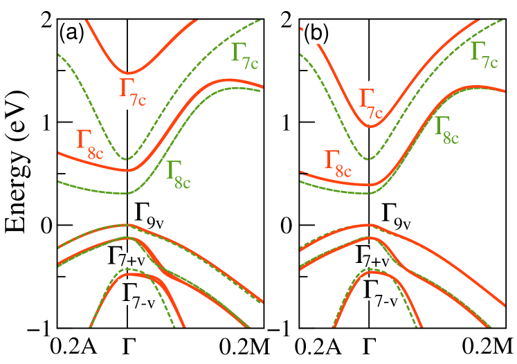
The QP band structures of hex-Si0.25Ge0.75 and of pure 2H-Ge with the lattice constants and the atomic positions of hex-Si0.25Ge0.75 are displayed in the panels (a) and (b), respectively, of Figs. 1. The electronic bands are plotted as a function of the vector along high-symmetry lines in the BZ, considering only a small region of the BZ around the point and zooming on the energy interval close to the direct band gap. We apply for clarity the symmetry classification of the Bloch states derived for lonsdaleite also to hex-Si0.25Ge0.75 and the distorted 2H-Ge cells, despite their symmetry reduction. The corresponding energy levels and band dispersions, i.e., the effective masses, near are given in Table 1. In the case of 2H-Ge the energies at perfectly agree with previous calculations using the same approach Rödl et al. (2019). This statement holds for the characteristic parameters of the splittings of the -like valence bands, the crystal-field splitting eV and the spin-orbit splittings eV and eV. The effective masses are however slightly increased, apart from those of along M. This is due to the strong sensitivity of the effective masses to the size of the -space volume around the -point considered to perform the parabolic fit of the band dispersion. The bands in Fig. 1(b), calculated for pure Ge using the atomic positions of the hex-SiGe cell, lead to only small variations with respect to the band structure of 2H-Ge. This especially holds for the valence bands. The conduction bands are slightly shifted toward higher energies as a consequence of the structural perturbation of the lonsdaleite lattice. Considering the reduction of the lattice constants, our findings are in qualitative agreement with results for a hydrostatic volume decrease shown in Ref. Suckert et al. (2021).
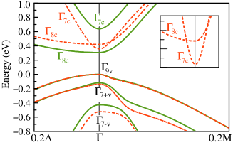
The largest shift happens for the second conduction band. More precisely, the changes of the atomic positions induce band shifts of 0.311 (), 0.061 (), 0.000 (), -0.010 (), and -0.032 () eV with respect to 2H-Ge (see Table 1). Totally different bands are instead obtained for uniaxially strained hex-Ge (1.8% tensile strain). In particular, this specific cell deformation leads to an inversion of the and conduction bands as visible in Fig. 2. This result is in agreement with earlier predictions Suckert et al. (2021). The resulting band energies are 0.358 (), 0.421 (), 0.000 (), -0.138 (), and -0.523 eV (). Because of the pure -character of the state, its energy drastically moves down toward the VBM, while the -containing conduction band only slightly shifts toward higher energies. This inversion of the two lowest conduction bands is in agreement with results of other strain studies for 2H-Ge Inaoka et al. (2015); Mellaerts et al. (2021) and also with the indirect-direct transition in 3C-Ge under tensile uniaxial strain Suckert et al. (2021).
. The band classification of the lonsdaleite symmetry group is also applied for the alloyed and structurally perturbed hex-Ge.
| position (eV) | effective mass () | ||||
|---|---|---|---|---|---|
| State | MBJLDA | HSE06 | M | K | A |
| 1.473 (0.639) | 1.559 (0.641) | 0.126 (0.055) | 0.132 (0.059) | 0.068 (0.048) | |
| 0.530 (0.306) | 0.561 (0.295) | 0.094 (0.093) | 0.099 (0.095) | 0.362 (1.098) | |
| 0.000 (0.000) | 0.000 (0.000) | 0.155 (0.092) | 0.311 (0.233) | 0.548 (0.516) | |
| -0.127 (-0.118) | -0.138 (-0.127) | 0.088 (0.072) | 0.087 (0.064) | 0.250 (0.120) | |
| -0.477 (-0.427) | -0.486 (-0.451) | 0.495 (0.242) | 0.419 (0.226) | 0.065 (0.048) | |
Mixing Si with Ge, in this case replacing 25% of the Ge atoms in the hexagonal cell, tends to increase significantly the band distances (see Fig. 1(a)), in agreement with the reduction of the atomic size from the covalent radius of 1.2 Å (Ge) to 1.11 Å (Si) Sargent-Welch (1980). The resulting structural modification may be interpreted as a compressive internal hydrostatic pressure of about 2.3% on the Ge lattice which opens the gap and interband distances. While this effect is small on the valence bands, the energy distances between conduction bands and their distances to the VBM are significantly increased, as it can be observed in Fig. 1(a) and Table 1. The comparison with the bands of pure 2H-Ge with atoms arranged as in hex-Si0.25Ge0.75, shown in Fig. 1(b), proves that the valence bands are negligibly affected by this simple structural perturbation. However, the conduction-band shifts toward higher energies are significantly enhanced by chemical perturbation, i.e., the replacement of a Ge atom by a Si one. The fundamental gap is opened from 0.31 to 0.53 eV. The splitting of the two lowest conduction bands dramatically increases from 0.33 to 0.94 eV. The gap opening is in agreement with photoluminescence (PL) measurements Fadaly et al. (2020) that indicate a shift of the PL peak position from 0.35 eV for pure Ge to 0.67 eV for Si0.35Ge0.65 in strong correlation with the fundamental gap variation in Table 1. The wavelength m corresponding to the fundamental gap of 2H-Ge is decreased to 1.85 m in hex-Si0.25Ge0.75. Incorporation of additional Si atoms may further reduce this wavelength toward the communication wavelength of 1.55 m. The corresponding gap eV should be reached for SixGe1-x with a composition applying linear gap interpolation. Similar values have been predicted elsewhere Fadaly et al. (2020); Borlido et al. (2021).
The modifications of band dispersion in Fig. 1, described around by the effective masses in Table 1, do not show a unique trend with the incorporation of Si into the Ge lattice. The uppermost conduction band and the three valence bands , , and exhibit an increase of the effective masses. Only the lowest conduction band maintains its dispersion along the direction perpendicular to the -axis but the effective electron mass parallel to the -axis is reduced. This behavior is probably related to the increasing repulsion between the two lowest conduction bands with rising , which also explains the increase of the energy distance .
Without considering modifications in the band occupation, optical spectra such as absorption or luminescence are determined by expressions of the type
| (1) |
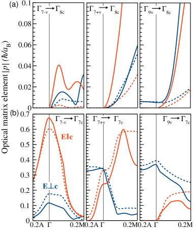
for light-polarization direction and photon energy . The optical transition matrix elements are plotted in Fig. 3 for all direct transitions between the three highest valence bands and the two lowest conduction bands along the high-symmetry directions M and A (see Fig. 1) in pure lonsdaleite Ge, hexagonal Si0.25Ge0.75 alloy and, for comparison, in hex-Ge with atomic positions determined by the alloy geometry. In Fig. 4 we present the optical transition matrix elements for hex-Ge under a tensile uniaxial strain of 1.8% with respect to the ideal lonsdaleite geometry.
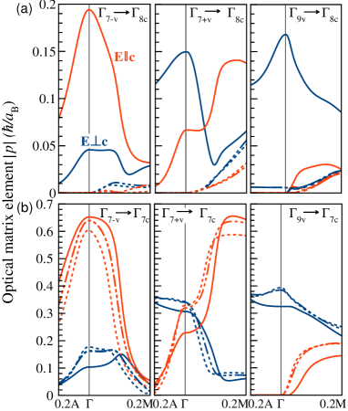
In the case of lonsdaleite Ge the curves in Fig. 3 agree with previous results Rödl et al. (2019). At they respect the selection rules imposed by group theory Tronc et al. (1999). All transitions from the -like valence bands into the -like second conduction band in Fig. 3(b) are allowed, independently of the light polarization direction. Only for light polarized parallel to the -axis, optical transitions from the uppermost valence band are forbidden. The situation is completely different for optical transitions involving the lowest conduction band , as it can be observed in Fig. 3(a). All transitions at are dipole-forbidden. The only exception is the transition for light polarization parallel to the -axis in agreement with group theory Tronc et al. (1999). However, the optical strength of the latter transition is by orders of magnitude, more precisely a factor of about 70, smaller than that of the transition. The origin of this disappointing result can be understood within the band-folding picture: the lowest conduction band of diamond Ge at two points is folded onto the point in the hexagonal BZ. Despite the modification of the atomic stacking in the hexagonal lattice compared with the diamond one, the strong -character of the states together with the accompanying vanishing oscillator strength between -type valence and conduction bands is mainly conserved. The orbital character of the lowest conduction band is illustrated by orbital and site projections of the wave function in Table 2. Each of the four Ge atoms in the lonsdaleite cell contribute equally and show a 70%, 20%, 10)% orbital character of . , -type, respectively.
Modifying pure 2H-Ge by replacing one Ge atom with Si to obtain hex-Si0.25Ge0.75, as shown in Fig. 3(b), leads to only small variations of the optical matrix elements of the transitions from the valence bands to the second-lowest conduction band. The situation is totally different for transitions into the lowest conduction band in Fig. 3(a). Apart from the band transition with light polarization parallel to the -axis, strong optical transitions appear in the alloyed system. Their dipole strengths are only smaller by factors of 2–3 compared to transitions to the band. Thereby the averaged contribution to the conduction band wave function is slightly increased (see Table 2). However, the four atoms in the Si1Ge3 unit cell give rise to drastically different contributions to the total wave function. According to Table 2, when the two Ge atoms lie above each other, bonded along the -axis, the -character of the "" wave function considerably increases up to 92%. Therefore strong intra-atomic contributions to the oscillator strengths are possible. Small lattice perturbations, such as due to the substitution of one Ge atom in lonsdaleite by an isoelectronic Si atom together with the accompanying symmetry reduction of the atomic positions, internal strain and stronger mixing-in of -orbitals into the lowest conduction band induce drastic changes in the optical oscillator strengths. The lowest optical transition becomes really dipole-allowed for in-plane polarization with a giant strength similar to that in typical optoelectronic materials like GaAs Bechstedt and Belabbes (2013).
| orbital | |||
|---|---|---|---|
| atom | |||
| 1 | 0.92, 0.70, 0.71 | 0.02, 0.20, 0.13 | 0.06, 0.10, 0.16 |
| 2 | 0.83, 0.70, 0.65 | 0.14, 0.20, 0.24 | 0.03, 0.10, 0.10 |
| 3 | 0.51, 0.70, 0.75 | 0.24, 0.20, 0.13 | 0.26, 0.10, 0.12 |
| 4 | 0.41, 0.70, 0.70 | 0.48, 0.20, 0.21 | 0.12, 0.10, 0.09 |
| average | 0.75, 0.70, 0.71 | 0.17, 0.20, 0.18 | 0.09, 0.10, 0.11 |
It is possible that structural and chemical perturbations may explain why in nanostructured Ge core-shell wires strong emission is experimentally observed already for nominally pure hexagonal Ge. Similar theoretical and experimental observations have been made for pseudodirect wurtzite semiconductors in comparison to indirect zinc-blende materials, e.g. for InP nanowires alloyed with Al Gagliano et al. (2018), or in wurtzite GaP nanowires, where strong many-body excitonic effects or tensile uniaxial strain may explain the measured strong luminescence Belabbes and Bechstedt (2019); Greil et al. (2016); Gagliano et al. (2016).
For a better understanding of the origin of the increased oscillator strengths we have separately considered the effect of a purely structural perturbation versus combined chemical and structural perturbation on lonsdaleite Ge. Considering the results in Fig. 3 and Table 2, we can conclude that the influence of the structural perturbation is much weaker than the chemical effect, despite the fact that Si and Ge are isovalent. The structural relaxation increases the interband transition energies in Fig. 1(b) and the oscillator strengths in Fig. 3. However, the effects are smaller as in the case of a concurrent chemical and structural modification, as in the hexagonal alloy Si0.25Ge0.75. The small changes of the momentum matrix elements are thereby in line with the minor variation of the orbital character in Table 2. The small effect of purely structural modifications cannot be generalized. In the case of moderate tensile uniaxial strain, as shown for 2H-Ge in Fig. 4, we can still report weak or moderate changes of the dipole strengths of the transitions , , , . In fact, in contrast to the band energies, the wave functions experience minor modifications under strain, and therefore the absolute values of the oscillator strenghts are nearly preserved. Following the trend with rising tensile uniaxial strain Suckert et al. (2021), an inversion of the two lowest conduction bands occurs, i.e., the conduction band appears below the band at . This band inversion leads to huge oscillator strengths for optical transitions to or from the lowest conduction band, similarly to what is shown in Fig. 3 for 2H-Ge and the second conduction band. A similar band inversion is suggested to happen in the band structure of the 4H polytype Raffy et al. (2002) of Ge Kiefer et al. (2010). Our own test calculations for 4H-Ge do not give rise to such a band inversion nor, consequently, strong optical transitions to or from the lowest conduction band. This finding is in agreement with the fact that the pure hexagonal stacking in 2H is mixed with a cubic stacking in the 4H polytype Raffy et al. (2002).
III Conclusions
In summary, we have clearly demonstrated by means of first-principles calculations that lonsdaleite germanium underlies a transition from a pseudo-direct semiconductor with a dipole-allowed but very weak optical oscillator strength into a direct semiconductor with typical strength of a transition, upon perturbation of the ideal hexagonal lattice. Here we consider the substitution of one Ge atom with a Si atom in the four atom unit cell. The alloying of 2H-Ge with Si leads not only to an increase of the interband transition energies but also to the enhancement of the dipole-matrix elements of all optical transitions from the three highest valence bands into the lowest conduction band, independently of light polarization. The increase of the oscillator strengths at leads to matrix elements of the order of those for transitions involving the second conduction band. Strong oscillator strengths of the lowest interband transitions also occur in uniaxially strained 2H-Ge because of the order inversion of the two lowest conduction bands. All in all, we conclude that perturbed lonsdaleite Ge is an excellent material for active optoelectronic applications in light-emitting diodes and lasers.
IV Computational Methods
The atomic configurations and lattice constants of the hexagonal crystals are optimized applying density functional theory (DFT) as implemented in the Vienna Ab-initio Simulation Package (VASP) Kresse and Furthmüller (1996) using the projector-augmented wave method Kresse and Joubert (1999) and a plane-wave cutoff of 500 eV. The shallow Ge3 electrons are treated as valence electrons. The modified Perdew-Becke-Ernzerhof (PBEsol) XC functional Perdew et al. (2008) is applied for structural relaxations. The BZ integration is performed using a -centered 12126 k-point grid. Atomic geometries are relaxed until the Hellmann-Feynman forces are below 1 meV/Å. The spin-orbit interaction is included for all electronic structure calculations.
Acknowledgments
We acknowledge financial support from the H2020-FETOpen projects SiLAS (grant agreement No. 735008) and OptoSilicon (grant agreement No. 964191).
Conflict of Interest
The authors declare no conflict of interest.
Data Availability Statement
The data that support the findings of this study are available on reasonable request from the corresponding author.
Keywords
germanium, silicon-germanium alloys, lonsdaleite, electronic structure, optical matrix elements, light emission
References
- Ball (2001) P. Ball, Nature 409, 1476 (2001), ISSN 1476–4687, URL https://doi.org/10.1038/35059301.
- Atabaki et al. (2018) A. H. Atabaki, S. Moazeni, F. Pavanello, H. Gevorgyan, J. Notaros, L. Alloatti, M. T. Wade, C. Sun, S. A. Kruger, H. Meng, et al., Nature 556, 349 (2018), URL https://doi.org/10.1038/s41586-018-0028-z.
- Raffy et al. (2002) C. Raffy, J. Furthmüller, and F. Bechstedt, Phys. Rev. B 66, 075201 (2002), URL http://link.aps.org/doi/10.1103/PhysRevB.66.075201.
- Fadaly et al. (2020) E. M. T. Fadaly, A. Dijkstra, J. R. Suckert, D. Ziss, M. A. J. van Tilburg, C. Mao, Y. Ren, V. T. van Lange, K. Korzun, S. Kölling, et al., Nature 580, 205 (2020), URL https://doi.org/10.1038/s41586-020-2150-y.
- Rödl et al. (2019) C. Rödl, J. Furthmüller, J. R. Suckert, V. Armuzza, F. Bechstedt, and S. Botti, Phys. Rev. Materials 3, 034602 (2019), URL https://link.aps.org/doi/10.1103/PhysRevMaterials.3.034602.
- Borlido et al. (2021) P. Borlido, J. R. Suckert, J. Furthmüller, F. Bechstedt, S. Botti, and C. Rödl, Phys. Rev. Materials 5, 114604 (2021), URL https://link.aps.org/doi/10.1103/PhysRevMaterials.5.114604.
- Cartoixà et al. (2017) X. Cartoixà, M. Palummo, H. I. T. Hauge, E. P. A. M. Bakkers, and R. Rurali, Nano Letters 17, 4753 (2017), pMID: 28654293, eprint https://doi.org/10.1021/acs.nanolett.7b01441, URL https://doi.org/10.1021/acs.nanolett.7b01441.
- Bao et al. (2021) N. Bao, F. Guo, D. Kang, Y. Feng, H. Wang, and J. Dai, Journal of Applied Physics 129, 145701 (2021), eprint https://doi.org/10.1063/5.0043773, URL https://doi.org/10.1063/5.0043773.
- Wang et al. (2021) Z. Wang, Z. Zhang, S. Liu, J. Robertson, and Y. Guo, Applied Physics Letters 118, 172101 (2021), eprint https://doi.org/10.1063/5.0044901, URL https://doi.org/10.1063/5.0044901.
- Bechstedt (2015) F. Bechstedt, Many-Body Approach to Electronic Excitations. Concepts and Applications (Springer-Verlag, Berlin, 2015).
- Tran et al. (2007) F. Tran, P. Blaha, and K. Schwarz, Journal of Physics: Condensed Matter 19, 196208 (2007), URL https://doi.org/10.1088/0953-8984/19/19/196208.
- Tran and Blaha (2009) F. Tran and P. Blaha, Phys. Rev. Lett. 102, 226401 (2009), URL https://link.aps.org/doi/10.1103/PhysRevLett.102.226401.
- Becke and Johnson (2006) A. D. Becke and E. R. Johnson, The Journal of Chemical Physics 124, 221101 (2006), eprint https://doi.org/10.1063/1.2213970, URL https://doi.org/10.1063/1.2213970.
- Laubscher et al. (2015) M. Laubscher, S. Küfner, P. Kroll, and F. Bechstedt, Journal of Physics: Condensed Matter 27, 405302 (2015), URL https://doi.org/10.1088/0953-8984/27/40/405302.
- Borlido et al. (2019) P. Borlido, T. Aull, A. W. Huran, F. Tran, M. A. L. Marques, and S. Botti, Journal of Chemical Theory and Computation 15, 5069 (2019), URL https://doi.org/10.1021/acs.jctc.9b00322.
- Borlido et al. (2020) P. Borlido, J. Schmidt, A. W. Huran, F. Tran, M. M. A. L. Marques, and S. Botti, npj Computational Materials 6, 96 (2020), URL https://doi.org/10.1038/s41524-020-00360-0.
- Heyd et al. (2003) J. Heyd, G. E. Scuseria, and M. Ernzerhof, J. Chem. Phys. 118, 8207 (2003), URL http://link.aip.org/link/?JCP/118/8207/1.
- Heyd et al. (2006) J. Heyd, G. E. Scuseria, and M. Ernzerhof, J. Chem. Phys. 124, 219906 (pages 1) (2006), URL http://link.aip.org/link/?JCP/124/219906/1.
- Gajdoš et al. (2006) M. Gajdoš, K. Hummer, G. Kresse, J. Furthmüller, and F. Bechstedt, Phys. Rev. B 73, 045112 (2006).
- Malone et al. (2010) B. D. Malone, S. G. Louie, and M. L. Cohen, Phys. Rev. B 81, 115201 (2010), URL https://link.aps.org/doi/10.1103/PhysRevB.81.115201.
- Suckert et al. (2021) J. R. Suckert, C. Rödl, J. Furthmüller, F. Bechstedt, and S. Botti, Phys. Rev. Materials 5, 024602 (2021), URL https://link.aps.org/doi/10.1103/PhysRevMaterials.5.024602.
- Inaoka et al. (2015) T. Inaoka, T. Furukawa, R. Toma, and S. Yanagisawa, Journal of Applied Physics 118, 105704 (2015), eprint https://doi.org/10.1063/1.4930225, URL https://doi.org/10.1063/1.4930225.
- Mellaerts et al. (2021) S. Mellaerts, V. Afanas’ev, J. W. Seo, M. Houssa, and J.-P. Locquet, ACS Applied Materials & Interfaces 13, 30941 (2021), URL https://doi.org/10.1021/acsami.1c03700.
- Sargent-Welch (1980) Sargent-Welch, Table of periodic properties of the elements (Skokie (Ill.), 1980).
- Tronc et al. (1999) P. Tronc, Y. Kitaev, G. Wang, M. Limonov, A. Panfilov, and G. Neu, physica status solidi (b) 216, 599 (1999).
- Bechstedt and Belabbes (2013) F. Bechstedt and A. Belabbes, Journal of Physics: Condensed Matter 25, 273201 (2013), URL https://doi.org/10.1088/0953-8984/25/27/273201.
- Gagliano et al. (2018) L. Gagliano, M. Kruijsse, J. D. D. Schefold, A. Belabbes, M. A. Verheijen, S. Meuret, S. Koelling, A. Polman, F. Bechstedt, J. E. M. Haverkort, et al., Nano Letters 18, 3543 (2018), URL https://doi.org/10.1021/acs.nanolett.8b00621.
- Belabbes and Bechstedt (2019) A. Belabbes and F. Bechstedt, physica status solidi (b) 256, 1800238 (2019), eprint https://onlinelibrary.wiley.com/doi/pdf/10.1002/pssb.201800238, URL https://onlinelibrary.wiley.com/doi/abs/10.1002/pssb.201800238.
- Greil et al. (2016) J. Greil, S. Assali, Y. Isono, A. Belabbes, F. Bechstedt, F. O. Valega Mackenzie, A. Y. Silov, E. P. A. M. Bakkers, and J. E. M. Haverkort, Nano Letters 16, 3703 (2016), URL https://doi.org/10.1021/acs.nanolett.6b01038.
- Gagliano et al. (2016) L. Gagliano, A. Belabbes, M. Albani, S. Assali, M. A. Verheijen, L. Miglio, F. Bechstedt, J. E. M. Haverkort, and E. P. A. M. Bakkers, Nano Letters 16, 7930 (2016), URL https://doi.org/10.1021/acs.nanolett.6b04242.
- Kiefer et al. (2010) F. Kiefer, V. Hlukhyy, A. J. Karttunen, T. F. Fässler, C. Gold, E.-W. Scheidt, W. Scherer, J. Nylén, and U. Häussermann, J. Mater. Chem. 20, 1780 (2010).
- Kresse and Furthmüller (1996) G. Kresse and J. Furthmüller, Phys. Rev. B 54, 11169 (1996).
- Kresse and Joubert (1999) G. Kresse and D. Joubert, Phys. Rev. B 59, 1758 (1999).
- Perdew et al. (2008) J. P. Perdew, A. Ruzsinszky, G. I. Csonka, O. A. Vydrov, G. E. Scuseria, L. A. Constantin, X. Zhou, and K. Burke, Phys. Rev. Lett. 100, 136406 (2008), URL https://link.aps.org/doi/10.1103/PhysRevLett.100.136406.