Photonic neuromorphic computing using vertical cavity semiconductor lasers
Abstract
Photonic realizations of neural network computing hardware are a promising approach to enable future scalability of neuromorphic computing. The number of special purpose neuromorphic hardware and neuromorphic photonics has accelerated on such a scale that one can now speak of a Cambrian explosion. Work along these lines includes (i) high performance hardware for artificial neurons, (ii) the efficient and scalable implementation of a neural network’s connections, and (iii) strategies to adjust network connections during the learning phase. In this review we provide an overview on vertical-cavity surface-emitting lasers (VCSELs) and how these high-performance electro-optical components either implement or are combined with additional photonic hardware to demonstrate points (i-iii). In the neurmorphic photonics’ context, VCSELs are of exceptional interest as they are compatible with CMOS fabrication, readily achieve 30% wall-plug efficiency and ¿30 GHz modulation bandwidth and hence are highly energy efficient and ultra-fast. Crucially, they react highly nonlinear to optical injection as well as to electrical modulation, making them highly suitable as all-optical as well as electro-optical photonic neurons. Their optical cavities are wavelength-limited, and standard semiconductor growth and lithography enables non-classical cavity configurations and geometries. This enables excitable VCSELs (i.e. spiking VCSELs) to finely control their temporal and spatial coherence, to unlock Terahertz bandwidths through spin-flip effects, and even to leverage cavity quantum electrodynamics to further boost their efficiency. Finally, as VCSEL arrays they are compatible with standard 2D photonic integration, but their emission vertical to the substrate makes them ideally suited for scalable integrated networks leveraging 3D photonic waveguides. Here, we discuss the implementation of spatially as well as temporally multiplexed VCSEL neural networks and reservoirs, computation on the basis of excitable VCSELs as photonic spiking neurons, as well as concepts and advances in the fabrication of VCSELs and microlasers. Finally, we provide an outlook and a road-map identifying future possibilities and some crucial milestones for the field.
I Introduction
Neural networks (NN) are concepts fundamentally relying on a connectionist approach to computation. This concept was developed based on the most-simplified features of a biological neuron, see Fig. 1(a). In a biological neuron, an axon typically forms a long-range link that connects via synapses to the dendrites of the post-synaptic neuron. Furthermore, a neuron’s inner working principles makes them respond nonlinearly to inputs. Following this principle, a NN creates and combines a large number of simple nonlinear transformations by artificial neurons, or perceptrons, while tweaking the network’s topology during a training phase such that specific computations result from emergence. This enables computing outside the classical symbolic programming and Boolean logic-gates catalogue: programming is replaced by statistical NN-topology optimization, while the hardware-concept is based on networks of simple nonlinear units rather than on mostly serial threads of logic gates. The increased flexibility in programming a computer enables addressing highly abstract computational challenges, and NNs currently drive a revolution in various areas of economy, technology and society. However, in a NN concept, all artificial neurons express their transformations of input signals simultaneously, which intimately links NNs to parallelism.
Today’s computing substrates can follow the connectionist principle only within tight limits, and the development of scalable, efficient, high performance hardware NNs currently is a major goal. The principle operations are information transformation, information transduction across the network connections, and topology optimization. Leveraging photons is highly promising for implementing the NN’s parallel interconnect Lohmann et al. (1996) and in particular in combination with photonic NN (PNN) computing Farhat et al. (1985); Shastri et al. (2021). In a photonic perceptron, see Fig. 1(b), optical inputs from the network are accumulated and nonlinearly transformed. Optical communication is inherently parallel Psaltis et al. (1990), energy efficient Miller (2017) and recent developments in optical memristors indicate a road-map towards efficient programmability Feldmann et al. (2021).
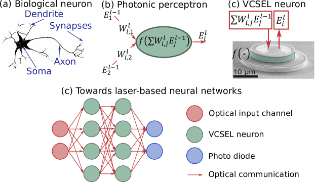
However, competitive nonlinear photonic components for artificial neurons have been a challenge. Lately, novel devices move the associated energy required consumption ever closer to electronics Liu et al. (2015), and a general strategy to enhance nonlinearity is to confine photons into a tight space or to increase the interaction time, often by using optical resonators such as the case for lasers. Vertical-cavity surface-emitting lasers (VCSELs) are one of the most prominent semiconductor lasers, with unique properties making them highly suitable for next generation PNN hardware, see Fig. 1(c) presenting an excerpt of a VCSEL during fabrication. VCSELs profit from high-yield and commercially mature fabrication, readily reaching above 30% wall-plug efficiency Haghighi and Lott (2021). Furthermore, due to their low lasing threshold currents and amplitude-phase coupling via Henry’s alpha factor, they react highly nonlinear to optical input and can therefore act as all-optical as well as electro-optical artificial neurons. VCSELs can readily be modulated with ¿30 GHz Haghighi and Lott (2021). Such high efficiency and high speed combined result in an ultra low energy per nonlinear transformation on the order of 10 fJ Heuser et al. (2020a). Considering the parallelism of a potentially passive and low-loss massive interconnect comprising connections per channel, this brings PNNs using VCSELs into the realm of ¡100 aJ per Operation, compared to 100 fJ1 pJ in electronic circuits. Crucially, this is only a current snapshot, and spin-VCSELs Lindemann et al. (2019) as well as high- VCSELs leveraging cavity quantum electrodynamics can further reduce this cost towards the fundamental physical limits on the order of a few photons per operation Wang et al. (2021).
VCSELs emit vertically to their substrates, which allows for efficient testing and for interfacing with scalable 3D integrated photonic circuits Moughames et al. (2020) or external optical resonators Brunner and Fischer (2015) in order to establish a PNN’s connections, see Fig. 1(d). Furthermore, in order to realize numerous photonic neurons they can be arranged in arrays Heuser et al. (2020a), or, as recently demonstrated, one can leverage spatial multiplexing of a multimode large area VCSEL in order to implement photonic neurons in spatial modes Porte et al. (2021a). An additional concept to extend the number of degrees of freedom are the two orthogonal polarization directions Vatin, Rontani, and Sciamanna (2019). Finally, VCSEL structures can be operated in an excitable regime, either relying on intra-cavity saturable absorbers Barbay, Kuszelewicz, and Yacomotti (2011) or on injection-locked induced excitability Hurtado and Javaloyes (2015).
Owing to their excellent properties, semiconductor laser-based PNNs have a long standing history Mos, Schleipen, and de Waardt (1997). Initially, the difficulties in training and implementing large neural networks limited the advance of the field. With the introduction of Reservoir Computing (RC) Jaeger and Haas (2004) this challenge was efficiently mitigated, and in combination with a temporal-multiplexing approach Appeltant et al. (2011) large-scale PNNs could be successfully emulated Van der Sande, Brunner, and Soriano (2017).
In this review, we provide a detailed overview on the implementation of VCSELs in different PNN topologies and different photonic neuron concepts. In Sec. III we discuss the temporal-multiplexing approach for PNNs, in Sec. IV the implementation of PNNs in spatially extended multimode lasers, while excitable photonic spiking VCSEL neurons are discussed in Sec. V, the fabrication of modern VCSELs structures in Sec. VI. At the end of our review we provide an extensive outlook in Sec. VII, which includes a roadmap to guide the field’s future development.
II Principles of a VCSEL
Photonic hardware provides neuromorphic computing with low-loss optical interconnects, intrinsic non-linearity and ultrafast operation rates Miller (2017). Suitable devices include optical modulators and different semiconductor lasers such as edge-emitting lasers, resonant tunnelling diode-laser-diode systems and VCSELs Prucnal et al. (2016); Tait et al. (2019). The latter are of particular interest because of their commercial availability, their compactness (in comparison to edge-emitters) and their vertical emission with close-to-ideal Gaussian emission profiles.
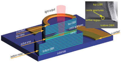
VCSELs can have many different configurations, yet they all feature identical design principles. Horizontally arranged high-reflectivity dielectric mirrors sandwich a gain material inside the cavity formed between the two mirror. Often, this cavity is very short and only half a wavelength in length. These planar structures are then etched to form pillars, or mesas, and optical emission is through the top-mirror that typically features a slightly lower reflectivity (99.8%). A schematic illustration of this principle is given in Fig. 2, and details of semiconductor VCSEL growth can be found in Sec. VI. Mirrors are usually distributed Bragg reflectors (DBR), comprising layers of different semiconductor materials transparent at the lasing wavelength yet with different refractive indices, while optical gain amplification can either be realized using one or more quantum wells or ensembles of quantum dots.
The dynamics of VCSELs are usually described using rate equation models. Compared to standard edge emitting semiconductor lasers, VCSEL’s do however require a more complex description, as they can commonly emit in and hence require modeling of orthogonal optical polarizations and the associated carrier spin-populations. The standard set of equations is based on the spin-flip model San Miguel, Feng, and Moloney (1995a). These features make their numerical description more complex, but this complexity is an assert for computation and allows for higher dimensionality or complexity of VCSEL-neurons and excitable behaviour, see Sect. V.
The most relevant parameters in such a description are the carrier’s relaxation oscillations, whose usual timescale of 0.1GHz typically determines the bandwidth of a VCSEL’s nonlinear transformation. Furthermore, if information is to be injected optically, then the usually ps lifetime of a photon within the VCSEL’s cavity is important. Optical information injection requires locking the VCSEL serving as photonic perceptron to an external injection laser Bueno et al. (2017). Such optical injection locking can only be realized inside a narrow range of frequency detuning between injection and response laser. The width of this detuning window is determined by the ratio of injection and the VCSEL’s emission power, and the VCSEL’s photon lifetime acts as a scaling factor: the longer the lifetime, the more frequency selective the VCSEL, and consequently the narrower the injection locking window is for a given power ratio.
III Time Delayed Reservoirs
The concept of delay-based reservoir computing was first introduced in a seminal paper of Appeltant et al. Appeltant et al. (2011). Mathematically, delay systems are described by delay differential equations whose temporal solution depends on the present as well as on past states. As such, when delayed feedback is added even a low-dimensional system offers the high-dimensional phase space which is the basis for RC. In contrast to spatially-extended RC systems, this approach uses only a single nonlinear node and a linear delayed feedback line with roundtrip duration as illustrated in Fig. 3(a). The nonlinear node continuously transforms the information fed back from the delay line. A number of virtual nodes (or virtual neurons) are then created by discretizing the continuous output of the delayed system in time segments of length , fulfilling the relation . Delay RC processes the input information sequentially and their operation speed is determined by the long delay length . Each input sample is mapped into the complete set of virtual nodes and multiplied by a random mask with periodicity . This temporal mask is introduced to diversify the response of the virtual nodes to the input signal and plays a similar role as the input weights in a conventional reservoir. Inertia Appeltant et al. (2011) or de-synchronization between injection mask length and delay Paquot et al. (2012) realize the reservoir’s internal connections. Typically, the input masking and the output layer weights are implemented off-line with a digital computer. The values (cf. Fig. 3(a)) are obtained one at a time in intervals of from the continuous analogue output, and they are calculated as a linear combination of the -spaced states of the virtual nodes, creating reservoir state x(t). The samples are then concatenated to state matrix where columns represent time and rows represent the neurons. The content of is therefore determined by the input, the masking, and the dynamical behavior of the nonlinear node.
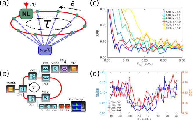
Delay-based RC aims at minimizing the expected hardware complexity of spatially-extended systems using a single nonlinear node only, a delay line and high-bandwidth capabilities for injection and detection. When implemented in photonics, delay-based RC systems have successfully been employed for classification, prediction and system modelling tasks with state-of-the-art results. Specific arguments photonic delayed RC implementations is the availability of off-the-shelf fiber-optics telecommunications hardware and that the lengths of the delay line does not impact the modulation bandwidth , cf. Fig. 3(b). The first optical hardware implementations of RC were independently developed by Larger et al. Larger et al. (2012) and Paquot et al. Paquot et al. (2012) using optoelectronic systems. Soon after, the first implementation with a semiconductor laser showed excellent performance for RC at Gbyte/s rates Brunner et al. (2013), the system’s injection locking parameter space was investigated in Bueno et al. (2017).
Implementations involving VCSELs leverage their polarization properties to improve the information processing performance and speed. Typically, one of the two optical modes dominates, but their relative intensities will change depending on laser, optical feedback and injection parameters. Time delayed RC based on VCSELs explore polarization dependencies to build alternative feedback schemes by rotating the polarization of the feedback or even exploring dual performance by simultaneously computing with the two modes. Vatin et al. numerically Vatin, Rontani, and Sciamanna (2018) and experimentally Vatin, Rontani, and Sciamanna (2019) first demonstrated delay-based RC with two-mode polarization dynamics of a VCSEL, which offers a bigger playground for optical feedback and injection configurations. Using either parallel (PAR) or orthogonal (ROT) configurations, a comprehensive experimental analysis can be found in Bueno et al. (2021), where the authors analyze the performance of both feedback configurations with Mackey-Glass prediction and nonlinear channel equalization tasks, see Fig. 3(c,d). The authors find that ROT feedback degrades the computational performance in terms of memory capacity when there is a significant power difference between the two emission modes Bueno et al. (2021).
Dual emission also offers the possibility of implementing two tasks in parallel, where each task is performed by one of the two perpendicularly polarized modes. This was first proposed numerically in Guo et al. (2019) and later on demonstrated experimentally in Vatin, Rontani, and Sciamanna (2020). Dual task operation slightly degrades the system’s performance for each task, but nevertheless represents an attractive advantage of VCSELs. Finally, Harkhoe et al. Harkhoe, Verschaffelt, and Van der Sande (2021) proposed and numerically investigated the use of fast spin-flip dynamics in VCSELs to boost the information processing speed at multi-GSa/s. The speed of the spin-flip dynamics, which depend on the birrefringence of the VCSEL, can further be increased by more than one order of magnitude Lindemann et al. (2019).
IV Spatio-temporal reservoirs
Delay-based reservoirs enable minimal hardware requirements Van der Sande, Brunner, and Soriano (2017), yet information is still processed sequentially, requiring the implementations of virtual, time multiplexed nodes Appeltant et al. (2011) and computational speed still depends on the size of a time-multiplexed PNN layer. It also entails that most implementations still rely on an external computer to pre-process data, construct the reservoir state and calculate the output weights for training. In Duport et al. (2012), an online learning strategy is implemented to reduce the influence of the external computer. However, the sequential nature remains a fundamental feature (and asset) of this system.
In contrast, by using large area VCSELs (LA-VCSELs), using a VCSEL with an aperture of and leveraging their highly multimode nature, a truly parallel, spatially multiplexed, VCSEL-based reservoir was introduced in Porte et al. (2021a). Due to parallelism, computing speed does in this system not depend on the PNN’s size any longer. In addition, an online learning strategy was implemented, making the system’s computation fully autonomous and relegating the external computer to a simple supervision and instrument-control role.
IV.1 Working principle and experimental setup
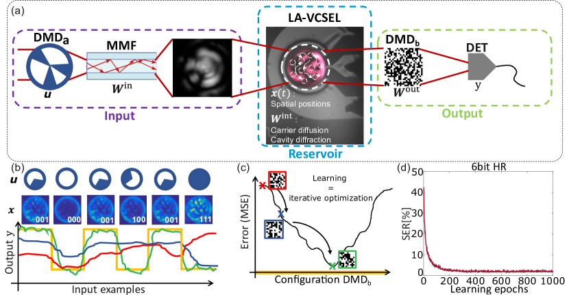
The PNN implemented in Porte et al. (2021a) can be divided into three sections, c.f. Fig. 4(a). First, the input layer is realised via a digital micromirror device (DMDa) and a multimode fibre (mmf). Spatial patterns (Boolean images) displayed on DMDa constitute the input information, in Fig. 4(a), and the mmf passively implements the PNN’s input weights via its complex transmission matrix.
The second part is the reservoir itself. The output field of the mmf is optically injected via imaging onto the LA-VCSEL top-facet, which implements all the components of the reservoir through its internal principles and nonlinear dynamics. Nodes are spatially multiplexed positions on the surface of the LA-VCSEL, and coupling is taken care of by carrier diffusion and optical diffraction inside the LA-VCSEL’s cavity. The reservoir state is then the perturbed mode-profile of the LA-VCSEL under optical injection, denoted in Fig. 4(a) as . In Fig. 4(b), the VCSEL’s response is shown for several 3-bit headers. Responses to each input pattern are complex, different, and non-trivial. This explains, in an intuitive sense, how finding a configuration of output weights that solve a certain computational task like header recognition, XOR, and digital-analogue conversion Porte et al. (2021a) is possible. Ultimately, the reservoir is used at speeds orders of magnitudes below its inherent timescales, and the LA-VCSEL was operated in it’s steady state, hence no recurrent properties such as fading memory of the device were exploited.
The last part of this PNN is its output layer. To implement output weights , the LA-VCSEL’s near field is imaged onto a second DMD (DMDb). The reflection off DMDb in one direction is imaged onto a large area detector, and the mirrors of DMDb sample the different positions, i.e. neurons on the LA-VCSEL’s surface. This applies a Boolean weight matrix to the reservoir state, and the authors implemented 90 trainable Boolean readout weights. The output of the network was recorded at the detector for a set of input patterns called the training batch. For each image in the training batch, the desired target output is known. Thus, after each training epoch (a run of one batch), is recorded and a normalized mean square error is calculated . Training is realised via a simple, yet effective evolutionary algorithm presented in Bueno et al. (2018); Andreoli et al. (2020). Boolean weights (mirrors) at random positions are flipped at the transition from to . If the change is beneficial, i.e. , it is kept, otherwise the output weights are reset to the configuration at epoch as shown in Fig. 4(b,c). This operation is repeated until the desired performance threshold is met. Figure 4(d) shows a representative learning curve for a 6bit header recognition task, the system reaches around a symbol error rate (SER).
IV.2 LA-VCSEL PNN metrics
The performance of the LA-VCSEL reservoir is extensively studied in Porte et al. (2021b), mapping the impact of several parameters on the overall performance. Figure 5(a) shows how the LA-VCSEL’s free running modes react to external optical injection. At nm, a resonance condition is met where the LA-VCSEL’s free running modes are suppressed (by ) and the device locks to the injection laser, that is to say, the VCSEL’s emission wavelength is shifted to that of the external drive laser. Injection locking has been extensively studied in Ackemann et al. (1999, 2000). In Fig. 5b), we see a clear dependence of the performance on the injection wavelength as well as the injection power ratio (), and the best performance is obtained under locking, consisten with Bueno et al. (2017) for a semiconductor laser delay reservoir.
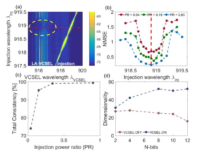
In addition, the authors link consistency, i.e. the ability of the system to respond in the same way when subjected to the same input, and dimensionality (numbers of degrees of freedom of the system) to the physical parameters , , and . Figure 5(c) shows the clear dependence of consistency on optical injection power, the total system consistency saturates and reaches an excellent level above .
In the same paper, a general way to gauge a system’s dimensionality was proposed. The same random input sequence is sent onto the LA-VCSEL, and the response of every neuron is recorded. The method relies on principal component analysis for noisy systems Malinowski (1977); Turner et al. (2006), and can generally be applied to other hardware ANNs. In Fig. 5(d), the dimensionality is measured for sequences of headers with the LA-VCSEL switched off as well as with the LA-VCSEL switched on. It is clear that the LA-VCSEL significantly increases the dimensionality of data representation. However, one has to say that rather than viewing the obtained dimensionality as absolute values, one should use their relative variation in direct comparisons, such as here to demonstrate the clear benefit of the LA-VCSEL on the PNN’s capability to expand the dimensionality of data representation. This is due to approximations made in Malinowski (1977); Turner et al. (2006) and due to a slightly heuristic criteria for assigning principle components to noise.
V Computing with Spiking VCSEL Neurons
A certain isomorphism between VCSELs and biological neurons has started to be explored. Here, we introduce VCSEL-based systems that are able to directly mimic (at ultrafast rates) the spiking action potentials of biological neurons and use the resulting photonic spiking signals to process information.
Biological neurons are known to communicate using electrical action potentials which take the form of temporal spiking signals. These are created when a neuron is subject to a stimulation from an external source or by neighbouring neurons. Remarkably, the generation of optical excitable spiking signals has also been observed in VCSELs, at ultrafast sub-nanosecond rates, multiple orders of magnitude faster than the time-scales of biological neurons Hurtado and Javaloyes (2015); Barbay, Kuszelewicz, and Yacomotti (2011). However, while the different nonlinear dynamical responses occurring in VCSELs, including excitability, have been widely reported in the literature, it is only in recent years that the link between the nonlinear effects in VCSELs and neuronal behaviour has been proposed Hurtado et al. (2010, 2012); Al-Seyab et al. (2014); Robertson et al. (2017); Deng, Robertson, and Hurtado (2017); Deng et al. (2018); Robertson et al. (2020a); Turconi et al. (2013); Robertson, Wade, and Hurtado (2019); Garbin, Tissoni, and Barland (2018); Dolcemascolo et al. (2018) towards novel paradigms in neuromorphic spike-based photonic processing systems.
V.1 Reports of excitability and neuronal responses in VCSELs
A first experimental report outlining the use of VCSELs as artificial photonic neurons appeared as early as 2010 Hurtado et al. (2010). That work described the use of optically-induced polarisation switching in a 1550 nm VCSEL to trigger different types of nonlinear activation functions, reproducing the response of neurons to excitatory and inhibitory stimuli. In a subsequent report in 2012 Hurtado et al. (2012), the link between the spiking dynamical responses triggered in VCSELs and those used to process information by neurons, was proposed. In that work, optical injection into the subsidiary (orthogonally-polarised) mode of a 1550 nm VCSEL induced polarisation switching. The authors investigated the polarization resolved dynamics of the stimulated VCSEL and showed responses reproducing different neuronal dynamics, such as phasic spiking and tonic spiking. This was the first implementation of a dynamically excited VCSEL-neuron yielding neural-like responses at sub-ns time-scales, a method that was further theorised in Al-Seyab et al. (2014) to explore the possibility of triggering excitable spiking responses in a VCSEL operating at the key telecom wavelength of 1550 nm. It was found that around the injection locking boundary (for both parallel and orthogonally-polarised optical injection), different excitable responses could be activated. Like in biological neurons excitable spikes had an activation threshold requirement, therefore revealing an experimental method of implementing controllable artificial VCSEL-based spiking neurons. The system was subsequently realised experimentally Hurtado and Javaloyes (2015), demonstrating that excitable neuron-like spiking dynamics could indeed be triggered in a 1550 nm-VCSEL with precise control. As theorized, short 0.5 ns input stimulations successfully triggered 100 ps-long spikes using both orthogonal and parallel polarized optical injection, revealing also a high reproducibility of the spiking outputs. The precise control of neuron-like excitability was also demonstrated through the manipulation of the injection modulation. It was shown that increasing the duration of the stimulation triggered the continuous firing of tonic spikes. In subsequent experimental reports, the authors reported also the achievement of spike inhibitory behaviour Robertson et al. (2017), communication of excitable spikes between coupled VCSEL-neurons Deng, Robertson, and Hurtado (2017); Deng et al. (2018) and their potentials for photonic spike memory operation and for the emulation of retinal neuronal circuits Robertson et al. (2020a).
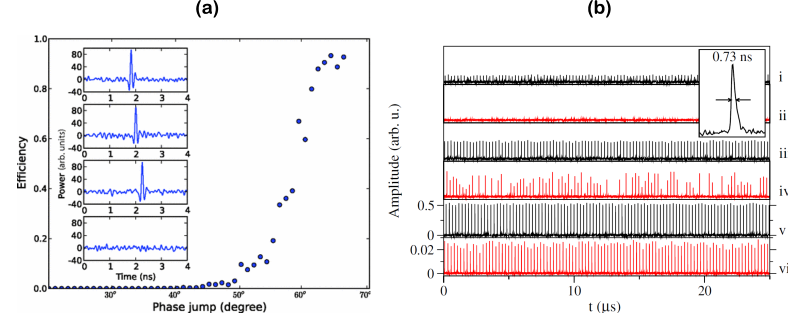
Excitable pulses have also been observed in short-wavelength VCSELs under phase-modulated optical injection. M. Turconi et al. Turconi et al. (2013) reported excitable pulses in a 980 nm VCSEL around the injection locking boundary when adding 100 ps-long phase jumps of different amplitudes in the optically injected signals. Fig. 6 a) shows the shape and efficiency of the phase-triggered excitable responses. Again, the excitable pulses required inputs to exceed an activation threshold for successful and consistent firing. The authors also showed that strong pulses in bias current could also trigger excitable responses from the VCSEL. The electrically-triggered spiking responses, however, were found to be less reliable and longer (typically 1 ns in duration) than those produced by optical injection with phase modulation. The activation of excitable spikes using the modulation of VCSEL bias current was again later demonstrated experimentally using VCSELs subject to intensity modulated optical injection Robertson, Wade, and Hurtado (2019). Using phase-modulation, Garbin et al. Garbin, Tissoni, and Barland (2018) also reported the regeneration of excitable optical spikes in a short-wavelength VCSEL under delayed optical feedback towards photonic spike memory operation. More recently, experimental and theoretical results successfully demonstrated resonator and integrator behaviour in phase modulated VCSEL systems producing multipulse excitability Dolcemascolo et al. (2018).
In parallel, excitable spiking signals have also been investigated in VCSELs containing intracavity saturable absorbers (SA). We refer to these devices from now onwards as VCSEL-SAs. Work led by Barbay et al. Barbay, Kuszelewicz, and Yacomotti (2011) has focused experimentally on spiking micro-pillar VCSEL-SA systems, demonstrating that optically-pumped micropillar VCSEL-SAs (with emission at 980 nm when optically pumped at 800 nm) exhibited self-pulsating (spiking) regimes immediately after their lasing threshold. Barbay et al. also demonstrated the activation of 730 ps-long excitable spikes under optical pump modulation (Fig. 6 b), and the existence of a spike activation threshold. In addition, this team also reported neuronal processing features in spiking micropillar VCSEL-SA structures, including spike firing latency, refractoriness and integration of multiple inputs prior to spike firing Selmi et al. (2014, 2015, 2016). These spiking behaviours were further confirmed by numerical simulations using the Yamada model for a semiconductor laser with a SA region. Numerical work by these authors also outlined the potentials of networks of evanescently coupled micropillar VCSEL-SAs to perform temporal spike logic operations (e.g. OR, AND) Pammi et al. (2019).
The activation of neuronal dynamics in VCSELs have also seen significant theoretical investigation via the SFM and Yamada models Yamada (1993); San Miguel, Feng, and Moloney (1995b). In addition to numerical work carried out by the teams at Strathclyde Hurtado and Javaloyes (2015); Robertson et al. (2017), Nice Dolcemascolo et al. (2018) and Paris Barbay, Kuszelewicz, and Yacomotti (2011); Selmi et al. (2016); Pammi et al. (2019), other groups also started to investigate numerically the spiking properties of VCSEL-neurons. In 2016, S. Xiang et al. Xiang, Wen, and Pan (2016) reported numerical results based on the SFM, validating the early 2012 experimental results of Hurtado et al. (2012), and later expanded on that experimental work to widely report theoretically on the potentials of dynamical polarisation switching responses in VCSELs for high-speed neuronal-like functionalities Xiang et al. (2017). In addition, a great body of theoretical work has recently appeared in literature focusing on optical spiking neurons based upon VCSEL-SAs Nahmias et al. (2013); Skontranis et al. (2021); Zhang et al. (2018a); Xiang et al. (2018a); Zhang et al. (2018b, 2020a); Xiang et al. (2018b, 2019); Song et al. (2020); Zhang et al. (2020b); Xiang et al. (2021, 2020). An early theoretical work Nahmias et al. (2013) used a two-section rate-equation model to describe a VCSEL-SA and demonstrate numerically that excitable pulses could be activated in these devices under the injection of short optical pulses. This work also revealed that VCSEL-SAs could theoretically operate as a leaky integrate-and-fire (LIF) neurons, and operate in different interconnected architectures with brain-inspired connectivity. Multiple other theoretical works further investigated the spiking responses in VCSEL-SAs and their potential for a wide diversity of tasks and procedures, ranging from spiking convolutional neural networks for image processing Skontranis et al. (2021), to spiking information encoding and storage Zhang et al. (2018a); Xiang et al. (2018a); Zhang et al. (2018b, 2020a), Sudoku solvers Gao et al. (2021), unsupervised learning procedures based on Spike-Timing Dependent Plasticity (STDP) Xiang et al. (2018b, 2019); Song et al. (2020), spike pattern recognition Zhang et al. (2020b); Xiang et al. (2021), spiking XOR gate implementations Xiang et al. (2020), amongst others.
V.2 Spike-based processing systems with VCSELs
It is only very recently that the first experimental demonstrators of spike processing systems, with VCSEL neurons for ultrafast neuromorphic photonic computing, have started to emerge Robertson et al. (2020b); Zhang et al. (2021a); Robertson et al. (2020c); Zhang et al. (2021b); Robertson et al. (2021); Hejda et al. (2020, 2020). Using VCSEL spiking neurons, several processing tasks, typical of artificial intelligence (AI) implementations, have been reported (e.g. image processing, and temporal pattern recognition) with the desired advantages of ultrafast processing times and low energy usage. In 2020, Robertson et al. Robertson et al. (2020b) demonstrated experimentally a method of classifying 4-bit digital patterns using a single VCSEL-neuron. In that work, as shown in Fig. 7 a, 4-bit patterns (with a bit rate of 150 ps) were injected optically into a VCSEL-neuron which fired fast 100 ps spikes only in response to target patterns, remaining quiescent otherwise. In the same work Robertson et al. (2020b), the authors used the leaky integrate-and-fire nature of a VCSEL-neuron to demonstrate experimentally a coincidence detection task, permitting the system to recognise the arrival of two different inputs within a very short temporal window (420 ps). Similarly, all-optical XOR classification has been demonstrated on binary patterns, emulating pyramidal neurons, using an optical injection system subject to dual modulation Zhang et al. (2021a).
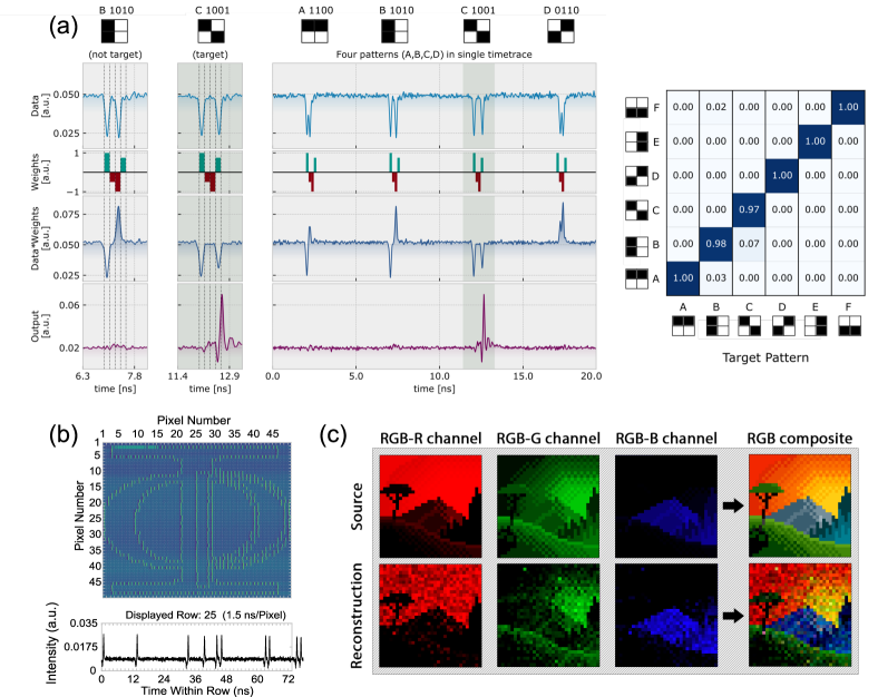
More recently, spiking VCSEL-neurons have also been applied for image processing. Experimental demonstrations of image edge-feature detection Robertson et al. (2020c) and binary convolution (that calculates the intensity gradients in images) Zhang et al. (2021b) with spiking VCSEL neurons have been reported. Notably, these different functionalities were achieved at high processing rates (with GHz’s input data signals) and low input power levels (tens of Ws), using hardware friendly systems and commercially available VCSELs. The latter reacted by triggering spikes (100 ps long) for image-pixels where specific features were detected, as shown in Fig. 7 b for the logo of the University of Strathclyde’s Institute of Photonics. Recent work by Robertson et al Robertson et al. (2021) has also shown that a single VCSEL-neuron can implement a full neuronal layer, performing image edge detection, by subsequently combining this photonic VCSEL layer with a software-implemented Spiking Neuronal Network (SNN). This hybrid VCSEL and software-implemented SNN demonstrated the accurate classification (97% precision) of complex images from the MNIST hand-written digit image database. These works showed spike processing rate of 1.5 ns/pixel using a single commercially-sourced VCSEL without any specific device design optimisation. Higher processing speeds and more complex functionalities are expected for bespoke device designs and systems using multiple VCSEL neurons simultaneously.
Additionally, recent work by Hejda et al Hejda et al. (2020) demonstrated experimentally the capability of spiking VCSEL-neurons to act as spike information encoders, using different spike coding mechanism, such as precise spike timing and spike rate encoding. Hejda et al demonstrated experimentally that VCSEL-neurons, like their biological counterparts, show a spike latency and inter-spike refractory period that is dependent on input stimulation amplitude. This was used to implement precise spike-timing encoding of digital signals (digital to spiking format conversion) at rates over 1 Gbps, and spike rate encoding, where the amplitude of an strong (weak) input stimulus yielded faster (slower) spike firing frequencies. In a subsequent work, Hejda et al Hejda et al. (2021) capitalised on the biologically-inspired rated coding ability of VCSEL-neurons, to demonstrate fast (nanosecond rate) encoding of image colour information for image processing functionalities (Fig. 7 c).
Artificial VCSEL-based optical neurons therefore provide exciting platforms towards fast (GHz rates) and low-energy neuromorphic photonic spike-processing systems. With access to threshold-and-fire and integrate-and-fire functionality, spiking VCSEL-neurons could be integrated into large interconnected photonic SNNs architectures for the implementation of complex light-enabled spike-based processing functionalities (e.g. image processing, computer vision, pattern recognition, etc.). VCSELs thus provide a consistent, all-optical, low power, and hardware friendly solution towards future ultrafast neuromorphic computing systems for AI technologies.
VI VCSEL and microlaser fabrication
The novel computing concepts discussed in this review rely crucially on vertically emitting lasers. VCSELs emit normal to the chip surface, can be controlled electrically, show high-speed dynamics and are energy efficient Michalzik (2012) and are much more compact than edge emitting lasers. In this regard, micropillar lasers are of high interest Gies and Reitzenstein (2019). These nanophotonic structures with diameters in the few-m range allow for the realization of photonic reservoirs consisting of hundreds or even thousands of small-scale lasers which can be coupled via external optical elements or integrated photonic structures. In addition to the small size footprint, microlasers offer the additional advantage that they operate in the regime of cavity quantum electrodynamics (cQED) which can reduce the threshold pump powers by orders of magnitude compared to conventional VCSELs to significantly improve the energy efficiency Bjork and Yamamoto (1991); Reitzenstein et al. (2008). Beyond that, quantum dot - micropillars can also act as bright electrically driven single-photon emitters Heindel et al. (2010); Schlehahn et al. (2016) which provides exciting opportunities towards quantum rneural networks. In the following technological aspects and the fabrication of VCSELs, microlasers and single photon emitters for applications in photonic neuromorphic computing are discussed.
VI.1 VCSEL fabrication
The fabrication of VCSELs requires multiple nanoprocessing steps. It starts with the epitaxial growth of a planar microresonator structure by means of molecular beam epitaxy (MBE) or metal-organic chemical vapour deposition (MOCDV). As schematically shown in Fig. 2 the microresonator is usually composed of a lower n-doped distributed Bragg reflector (DBR), the central cavity layer which is at least a thick and includes the active area, and the upper p-doped DBR Liu et al. (2015). In the often used GaAs material system, the DBRs consists of typically more than 20 -thick AlGaAs/GaAs layers and the active medium in the central GaAs cavity is usually based on multiple InGaAs quantum wells located at the antinode of the confined light field Michalzik (2012). In addition, the central cavity includes at least one thin AlGaAs layer with high Al-content (¿90%), which is later oxidized and acts as current window and leads to lateral light confinement governing the emission beam profile. The lateral nanoprocessing of VCSEL devices starts with the patterning of circular mesa structures with diameters in the range of 20 - 30 m by means of UV lithography and plasma etching. Next, the current aperture with a well-defined inner diameter is formed by wet thermal oxidation of the cavity-integrated AlGaAs layer. Finally the lower n-contact and the upper ring-shaped p-contact are realized by additional UV lithography steps and metal deposition, leading to a VCSEL device as depicted in Fig. 2. It is noteworthy that especially in case of long wavelength VCSELs, intracavity contacts are preferred to avoid optical losses due to free-carrier absorption in the doped DBRs Mehta et al. (2006)..
Beyond individual VCSELs, which have are today standard components for optical data communication, VCSEL arrays have become more and more important in recent years, finding applications for example in face recognition in modern cell phones Liu et al. (2019). Moreover, they are highly attractive to implement photonic reservoir computing and schemes relying on fast optical matrix multiplication using 1D VCSEL arrays Hamerly et al. (2019). While VCSEL arrays are in principle commercially available, neuromorphic applications have specific requirements which demand the development of customized VCSEL arrays with special geometry and optical properties.
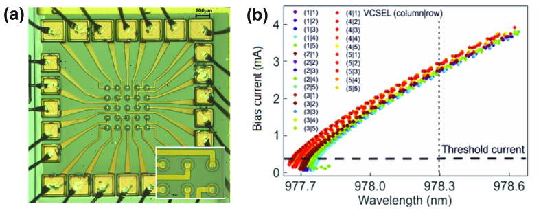
One example is a 5 x 5 VCSEL array optimized for photonic reservoir computing based on the diffractive coupling of VCSELs Brunner and Fischer (2015). Generally, neuromorphic computing concept require dense and spectrally homogenous VCSEL arrays, which in turn requires specific design and fabrication. One example of such an array is shown in Fig. 8(a). The 55 array includes 25 VCSELs with a pitch of only 80 m, which is significantly smaller compared to commercial arrays. Dense packing facilitates efficient diffractive coupling within a available optical field of view Maktoobi et al. (2020). Additionally, the wafer material was chosen to guarantee a high spectral homogeneity, which is essential to allow for locking all VCSELs to an external injection laser. As can be seen in Fig. 8(b), the emission wavelengths of the 25 VCSELs can be fine-tuned by the injection current of each individual emitter Heuser et al. (2020a). This enables a spectral homogeneity matching the injection locking range of 10-20 GHz. Moreover, due to a slight ellipticity of the emitters’ cross-section, excellent polarization control of the 25 VCSELs is obtained with a standard deviation of only 1.5∘.
VI.2 High- microlaser and dense microlaser arrays
Even VCSELs still pose limitations, not only in terms of the size-footprint, but also regarding the energy efficiency and modulation speed. To overcome such limitations, it is interesting to consider micro- and nanolasers which operate in the regime of cQED Chow and Reitzenstein (2018). Here, small mode volumes and high cavity quality factors lead to enhanced light matter interaction which is quantified by the Purcell factor. The Purcell effect leads to a high fraction of spontaneous emission coupled into the lasing mode, which is described in terms of the -factor and which leads to an order of magnitude reduction of the threshold pump power when comparing cavity-enhance high- micro- and nano-lasers with conventional semiconductor lasers Bjork and Yamamoto (1991). Additionally, the tight mode confinement in microlasers gives the opportunity to efficiently control the emission features such as the emission wavelength by the geometry of the laser cavity.
Micropillar lasers with quantum dot (QD) gain medium are a popular type of microlasers Gies and Reitzenstein (2019). Alike to VCSEL devices, they emit vertically, and they can be driven electrically in a straightforward way Böckler et al. (2008). In fact, large-scale micropillar arrays with small size footprint and high spectral homogeneity are ideally suited to realize the PRC proposed in Ref. Brunner and Fischer (2015). To meet the requirements of this neuromorphic computing scheme the QD-micropillar array has to feature a small pitch below 10 m and high spectral homogeneity on a scale of the injecting locking range of a few tens of GHz, i.e. the spectral homogeneity of the array must be better than about 200 V.
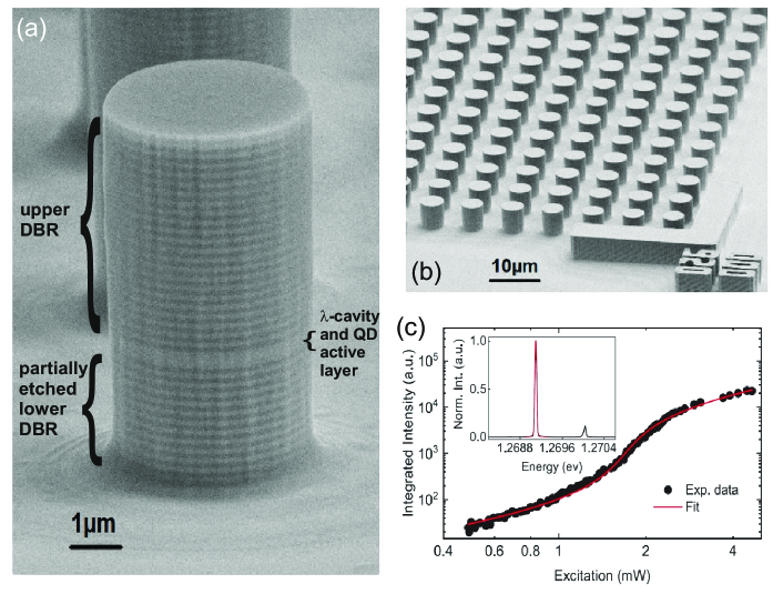
In order to fulfill the said requirements, the microlaser-arrays have to be fabricated by state-of-the-art nanotechnology platforms. Similar to VCSEL devices QD micropillar lasers are typically based on an epitaxial planar AlGaAs/GaAs microcavity structure with a lower and an upper DBR with up to 30 mirror pairs in an asymmetric design (3-4 more mirror pairs in the lower DBR to ensure directional emission via the upper DBR) and a central GaAs cavity, usually with a thickness of and a single layer of self-assembled InGaAs QDs at the field antinode for optical gain. Fig. 9(a) shows a scanning electron microscopy (SEM) image of a QD-micropillar with a lower (upper) DBR composed of 27 and (23) /4-thick Al0.9Ga0.1As/GaAs mirror pairs Heuser et al. (2020b). The lower DBR is only partially (12 mirror pairs) etched, which is, however, sufficient to obtain the desired tight mode confinement, while maintaining a high Q-factor. Using electron beam lithography and plasma etching, dense arrays of such micropillar cavities can be realized with high accuracy. Fig. 9(b) shows an excerpt of such an array consisting of 30 x 30 QD-micropillars with a pitch of 8.3 m.
An exemplary emission spectrum of an optically pumped QD-micropillar laser is depicted in the inset of Fig. 9(c). It is dominated by emission of the fundamental pillar mode HE11 at about 1.269 eV. The input-output dependence of the fundamental emission mode is plotted in Fig. 9(b) in double-logarithmic scale. The observed s-shaped behavior with a small non-linearity above the threshold pump power of about 1.8 mW is typical for cavity-enhanced microlasers. Fitting the experimental data with a rate-equations laser model allows us to extract a -factor of 2%. Higher -factors close to unity can be obtained for QD-micropillars with smaller diameter and adiabatic microcavity design.
Unfortunately, epitaxially grown micro-cavity wafers usually suffer from, both, a radial spectral dependence and local spectral inhomogeneities on a scale greater than what is acceptable for PRC. To address this issue and to reduce the spectral inhomogeneities of micropillar arrays advanced nanotechnology steps have to be applied for their fabrication. An interesting approach is “diameter tuning“ which takes advantage of the thigh mode confinement in micropillar cavities to precisely adjust the emission energy of each pillar in the array via its diameter during fabrication to compensate wafer inhomogeneities Heuser et al. (2018, 2020b). There, the emission energy of the respective microcavity area is first recorded with m accuracy by micro-photoluminesence (PL) mapping relative to alignment markers (see lower right corner in Fig. 9(b) for such a marker structure). With the knowledge of the local emission energie, the diameter of each micropillar is calculated where small (large) pillar diameters blue (red) shift its emission energy towards the target emission energy to compensate the spectral inhomogeneity of the underlying microcavity. As a result, after electron beam lithography and plasma etching, the spectral spread of emission energy of the micropillars in the fabricated arrays can be reduced from 1 meV to values as low as 120 eV Heuser et al. (2020b). These results is very promising and further enhancement of the spectral homogeneity of large scale QD-micropillar arrays is expected by improved growth and nanoprocessing capabilities.
VII Outlook
The application of standard and more advanced VCSELs in various neuromorphic computing concepts and schemes is by now an established approach, with clearly identified merits and future positibilities. Similar to other areas in neuromorphic photonics, the crucuial future steps are now an increasingly seamless interfacing and integration with other techniques in order to form complete computing systems. Crucial aspects here are (i) photonic integration, and (ii) more or less autonomous operation demonstrating a clear benefit in a relevant performance metric compared to other, and most importantly, to electronic neurmorphic computing concepts.
Funding
The authors acknowledge the support of the Region Bourgogne Franche-Comté. This work was supported by the EUR EIPHI program (Contract No. ANR-17-EURE- 0002), by the Volkwagen Foundation (NeuroQNet I&II), by the French Investissements d’Avenir program, project ISITE-BFC (contract ANR-15-IDEX-03), partly by the french RENATECH network and its FEMTO-ST technological facility, and by the European Union’s Horizon 2020 research and innovation program under the Marie Skłodowska-Curie grant agreement No 713694 (MULTIPLY) and 860830 (POST DIGITAL).
Disclosures
The authors declare no conflicts of interest.
References
- Lohmann et al. (1996) A. W. Lohmann, R. G. Dorsch, D. Mendlovic, C. Ferreira, and Z. Zalevsky, Journal of the Optical Society of America A 13, 470 (1996).
- Farhat et al. (1985) N. H. Farhat, D. Psaltis, A. Prata, and E. Paek, Applied Optics 24, 1469 (1985).
- Shastri et al. (2021) B. J. Shastri, A. N. Tait, T. Ferreira de Lima, W. H. P. Pernice, H. Bhaskaran, C. D. Wright, and P. R. Prucnal, Nature Photonics 15, 102 (2021).
- Psaltis et al. (1990) D. Psaltis, D. Brady, X.-G. Gu, and S. Lin, Nature 343, 325 (1990).
- Miller (2017) D. A. Miller, Journal of Lightwave Technology 35, 346 (2017), arXiv:1609.05510 .
- Feldmann et al. (2021) J. Feldmann, N. Youngblood, M. Karpov, H. Gehring, X. Li, M. Stappers, M. Le Gallo, X. Fu, A. Lukashchuk, A. S. Raja, J. Liu, C. D. Wright, A. Sebastian, T. J. Kippenberg, W. H. P. Pernice, and H. Bhaskaran, Nature 589, 52 (2021), 2002.00281 .
- Liu et al. (2015) K. Liu, C. R. Ye, S. Khan, and V. J. Sorger, Laser and Photonics Reviews 9, 172 (2015).
- Haghighi and Lott (2021) N. Haghighi and J. A. Lott, Materials 14, 397 (2021).
- Heuser et al. (2020a) T. Heuser, M. Pflüger, I. Fischer, J. A. Lott, D. Brunner, and S. Reitzenstein, Journal of Physics: Photonics 2, 044002 (2020a).
- Lindemann et al. (2019) M. Lindemann, G. Xu, T. Pusch, R. Michalzik, M. R. Hofmann, I. Žutić, and N. C. Gerhardt, Nature 568, 212 (2019).
- Wang et al. (2021) T. Wang, S.-Y. Ma, L. G. Wright, T. Onodera, B. Richard, and P. L. McMahon, (2021), arXiv:2104.13467 .
- Moughames et al. (2020) J. Moughames, X. Porte, M. Thiel, G. Ulliac, M. Jacquot, L. Larger, M. Kadic, and D. Brunner, Optica 7, 640 (2020), 1912.08203 .
- Brunner and Fischer (2015) D. Brunner and I. Fischer, Optics letters 40, 3854 (2015).
- Porte et al. (2021a) X. Porte, A. Skalli, N. Haghighi, S. Reitzenstein, J. A. Lott, and D. Brunner, Journal of Physics: Photonics 3, 024017 (2021a).
- Vatin, Rontani, and Sciamanna (2019) J. Vatin, D. Rontani, and M. Sciamanna, Optics express 27, 18579 (2019).
- Barbay, Kuszelewicz, and Yacomotti (2011) S. Barbay, R. Kuszelewicz, and A. M. Yacomotti, Optics Letters 36, 4476 (2011).
- Hurtado and Javaloyes (2015) A. Hurtado and J. Javaloyes, Applied Physics Letters 107, 241103 (2015).
- Mos, Schleipen, and de Waardt (1997) E. C. Mos, J. J. H. B. Schleipen, and H. de Waardt, Applied Optics 36, 6654 (1997).
- Jaeger and Haas (2004) H. Jaeger and H. Haas, Science 304, 78 (2004).
- Appeltant et al. (2011) L. Appeltant, M. C. Soriano, G. V. D. Sande, J. Danckaert, S. Massar, J. Dambre, B. Schrauwen, C. R. Mirasso, I. Fischer, G. Van der Sande, J. Danckaert, S. Massar, J. Dambre, B. Schrauwen, C. R. Mirasso, and I. Fischer, Nature communications 2, 468 (2011).
- Van der Sande, Brunner, and Soriano (2017) G. Van der Sande, D. Brunner, and M. C. Soriano, Nanophotonics 6, 561 (2017).
- Prucnal et al. (2016) P. R. Prucnal, B. J. Shastri, T. F. de Lima, M. A. Nahmias, and A. N. Tait, Advances in Optics and Photonics 8, 228 (2016).
- Tait et al. (2019) A. N. Tait, T. F. de Lima, M. A. Nahmias, H. B. Miller, H.-T. Peng, B. J. Shastri, and P. R. Prucnal, Physical Review Applied 11 (2019), 10.1103/physrevapplied.11.064043.
- San Miguel, Feng, and Moloney (1995a) M. San Miguel, Q. Feng, and J. V. Moloney, Physical Review A 52, 1728 (1995a).
- Bueno et al. (2017) J. Bueno, D. Brunner, M. Soriano, and I. Fischer, Optics Express 25, 2401 (2017).
- Paquot et al. (2012) Y. Paquot, F. Duport, A. Smerieri, J. Dambre, B. Schrauwen, M. Haelterman, and S. Massar, Scientific Reports 2, 287 (2012), arXiv:1111.7219 .
- Bueno et al. (2021) J. Bueno, J. Robertson, M. Hejda, and A. Hurtado, IEEE Photonics Technology Letters (2021).
- Larger et al. (2012) L. Larger, M. C. Soriano, D. Brunner, L. Appeltant, J. M. Gutierrez, L. Pesquera, C. R. Mirasso, and I. Fischer, Optics express 20, 3241 (2012), arXiv:9605103 [cs] .
- Brunner et al. (2013) D. Brunner, M. C. Soriano, C. R. Mirasso, and I. Fischer, Nature communications 4, 1364 (2013).
- Vatin, Rontani, and Sciamanna (2018) J. Vatin, D. Rontani, and M. Sciamanna, Optics Letters 43, 4497 (2018).
- Guo et al. (2019) X. X. Guo, S. Y. Xiang, Y. H. Zhang, L. Lin, A. J. Wen, and Y. Hao, IEEE Journal of Selected Topics in Quantum Electronics 26, 1 (2019).
- Vatin, Rontani, and Sciamanna (2020) J. Vatin, D. Rontani, and M. Sciamanna, APL Photonics 5, 086105 (2020).
- Harkhoe, Verschaffelt, and Van der Sande (2021) K. Harkhoe, G. Verschaffelt, and G. Van der Sande, Applied Sciences 11, 4232 (2021).
- Duport et al. (2012) F. Duport, B. Schneider, A. Smerieri, M. Haelterman, and S. Massar, Optics express 20, 22783 (2012).
- Porte et al. (2021b) X. Porte, A. Skalli, N. Haghighi, S. Reitzenstein, J. A. Lott, and D. Brunner, submitted to Optical Materials Express X, X (2021b).
- Bueno et al. (2018) J. Bueno, S. Maktoobi, L. Froehly, I. Fischer, M. Jacquot, L. Larger, and D. Brunner, Optica 5, 756 (2018).
- Andreoli et al. (2020) L. Andreoli, X. Porte, S. Chrétien, M. Jacquot, L. Larger, and D. Brunner, Nanophotonics 9, 4139 (2020).
- Ackemann et al. (1999) T. Ackemann, S. Barland, M. Cara, M. Giudici, and S. Balle, in Nonlinear Guided Waves and Their Applications (Optical Society of America, 1999) p. WC4.
- Ackemann et al. (2000) T. Ackemann, S. Barland, M. Giudici, J. R. Tredicce, S. Balle, R. Jaeger, M. Grabherr, M. Miller, and K. J. Ebeling, physica status solidi (b) 221, 133 (2000).
- Malinowski (1977) E. R. Malinowski, Analytical Chemistry 49, 606 (1977).
- Turner et al. (2006) D. Turner, R. Knuteson, H. Revercomb, C. Lo, and R. Dedecker, Journal of Atmospheric and Oceanic Technology 23, 1223 (2006).
- Hurtado et al. (2010) A. Hurtado, A. Quirce, A. Valle, L. Pesquera, and M. J. Adams, Opt. Express 18, 9423 (2010).
- Hurtado et al. (2012) A. Hurtado, K. Schires, I. D. Henning, and M. J. Adams, Applied Physics Letters 100, 103703 (2012).
- Al-Seyab et al. (2014) R. Al-Seyab, I. D. Henning, M. J. Adams, and A. Hurtado, Conference Digest - IEEE International Semiconductor Laser Conference , 165 (2014).
- Robertson et al. (2017) J. Robertson, T. Deng, J. Javaloyes, and A. Hurtado, Opt. Lett. 42, 1560 (2017).
- Deng, Robertson, and Hurtado (2017) T. Deng, J. Robertson, and A. Hurtado, IEEE Journal of Selected Topics in Quantum Electronics 23 (2017), 10.1109/JSTQE.2017.2685140.
- Deng et al. (2018) T. Deng, J. Robertson, Z.-M. Wu, G.-Q. Xia, X.-D. Lin, X. Tang, Z.-J. Wang, and A. Hurtado, IEEE Access 6 (2018), 10.1109/ACCESS.2018.2878940.
- Robertson et al. (2020a) J. Robertson, E. Wade, Y. Kopp, J. Bueno, and A. Hurtado, IEEE Journal of Selected Topics in Quantum Electronics 26 (2020a), 10.1109/JSTQE.2019.2931215.
- Turconi et al. (2013) M. Turconi, B. Garbin, M. R. Feyereisen, M. Giudici, and S. Barland, Physical review. E, Statistical, nonlinear, and soft matter physics 88 2, 22923 (2013).
- Robertson, Wade, and Hurtado (2019) J. Robertson, E. Wade, and A. Hurtado, IEEE Journal of Selected Topics in Quantum Electronics 25 (2019), 10.1109/JSTQE.2019.2899040.
- Garbin, Tissoni, and Barland (2018) B. Garbin, G. Tissoni, and S. Barland, Cybernetics and Physics 7 3, 96 (2018).
- Dolcemascolo et al. (2018) A. Dolcemascolo, B. Garbin, B. Peyce, R. Veltz, and S. Barland, Phys. Rev. E 98, 62211 (2018).
- Selmi et al. (2014) F. Selmi, R. Braive, G. Beaudoin, I. Sagnes, R. Kuszelewicz, and S. Barbay, Phys. Rev. Lett. 112, 183902 (2014).
- Selmi et al. (2015) F. Selmi, R. Braive, G. Beaudoin, I. Sagnes, R. Kuszelewicz, and S. Barbay, Opt. Lett. 40, 5690 (2015).
- Selmi et al. (2016) F. Selmi, R. Braive, G. Beaudoin, I. Sagnes, R. Kuszelewicz, T. Erneux, and S. Barbay, Phys. Rev. E 94, 42219 (2016).
- Pammi et al. (2019) V. A. Pammi, K. Alfaro-Bittner, M. G. Clerc, and S. Barbay, IEEE Journal of Selected Topics in Quantum Electronics 26, 1 (2019).
- Yamada (1993) M. Yamada, IEEE Journal of Quantum Electronics 29, 1330 (1993).
- San Miguel, Feng, and Moloney (1995b) M. San Miguel, Q. Feng, and J. V. Moloney, Phys. Rev. A 52, 1728 (1995b).
- Xiang, Wen, and Pan (2016) S. Xiang, A. Wen, and W. Pan, IEEE Photonics Journal 8 (2016), 10.1109/JPHOT.2016.2614104.
- Xiang et al. (2017) S. Y. Xiang, H. Zhang, X. X. Guo, J. F. Li, A. J. Wen, W. Pan, and Y. Hao, IEEE Journal of Selected Topics in Quantum Electronics 23 (2017), 10.1109/JSTQE.2017.2678170.
- Nahmias et al. (2013) M. A. Nahmias, B. J. Shastri, A. N. Tait, and P. R. Prucnal, IEEE Journal of Selected Topics in Quantum Electronics 19, 1 (2013).
- Skontranis et al. (2021) M. Skontranis, G. Sarantoglou, S. Deligiannidis, A. Bogris, and C. Mesaritakis, Applied Sciences 11 (2021), 10.3390/app11041383.
- Zhang et al. (2018a) Y. Zhang, S. Xiang, J. Gong, X. Guo, A. Wen, and Y. Hao, Applied Optics 57, 1731 (2018a).
- Xiang et al. (2018a) S. Xiang, Y. Zhang, X. Guo, A. Wen, and Y. Hao, Journal of Lightwave Technology 36 (2018a), 10.1109/JLT.2018.2818195.
- Zhang et al. (2018b) Y. Zhang, S. Xiang, X. Guo, A. Wen, and Y. Hao, Scientific Reports 2018 8:1 8, 1 (2018b).
- Zhang et al. (2020a) Z. Zhang, Z. Wu, D. Lu, G. Xia, and T. Deng, Nonlinear Dynamics 99, 1103 (2020a).
- Xiang et al. (2018b) S. Xiang, J. Gong, Y. Zhang, X. Guo, Y. Han, A. Wen, and Y. Hao, IEEE Journal of Quantum Electronics 54 (2018b), 10.1109/JQE.2018.2879484.
- Xiang et al. (2019) S. Xiang, Y. Zhang, J. Gong, X. Guo, L. Lin, and Y. Hao, IEEE Journal of Selected Topics in Quantum Electronics 25, 1 (2019).
- Song et al. (2020) Z. Song, S. Xiang, Z. Ren, G. Han, and Y. Hao, IEEE Journal of Selected Topics in Quantum Electronics 26, 1 (2020).
- Zhang et al. (2020b) Y. Zhang, S. Xiang, X. Guo, A. Wen, and Y. Hao, Journal of Lightwave Technology 38, 5071 (2020b).
- Xiang et al. (2021) S. Xiang, Z. Ren, Z. Song, Y. Zhang, X. Guo, G. Han, and Y. Hao, IEEE Transactions on Neural Networks and Learning Systems 32, 2494 (2021).
- Xiang et al. (2020) S. Xiang, Z. Ren, Y. Zhang, Z. Song, and Y. Hao, Optics letters 45, 1104 (2020).
- Gao et al. (2021) S. Gao, S. Xiang, Z. Song, Y. Han, and Y. Hao, Optics Communications 495, 127068 (2021).
- Robertson et al. (2020b) J. Robertson, M. Hejda, J. Bueno, and A. Hurtado, Scientific Reports 10 (2020b), 10.1038/s41598-020-62945-5.
- Zhang et al. (2021a) Y. Zhang, S. Xiang, X. Cao, S. Zhao, X. Guo, A. Wen, and Y. Hao, Photon. Res. 9, 1055 (2021a).
- Robertson et al. (2020c) J. Robertson, Y. Zhang, M. Hejda, J. Bueno, S. Xiang, and A. Hurtado, Optics Express 28, 37526 (2020c).
- Zhang et al. (2021b) Y. Zhang, J. Robertson, S. Xiang, M. Hejda, J. Bueno, and A. Hurtado, Photonics Research 9, B201 (2021b).
- Robertson et al. (2021) J. Robertson, P. Kirkland, J. A. Alanis, M. Hejda, J. Bueno, G. D. Caterina, and A. Hurtado, arXiv 2110.01617 (2021).
- Hejda et al. (2020) M. Hejda, J. Robertson, J. Bueno, and A. Hurtado, JPhys Photonics 2 (2020), 10.1088/2515-7647/aba670.
- Hejda et al. (2021) M. Hejda, J. Robertson, J. Bueno, J. A. Alanis, and A. Hurtado, APL Photonics 6, 060802 (2021).
- Michalzik (2012) R. Michalzik, in Springer Series in Optical Sciences (Springer Berlin Heidelberg, 2012) pp. 19–75.
- Gies and Reitzenstein (2019) C. Gies and S. Reitzenstein, Semiconductor Science and Technology 34, 073001 (2019).
- Bjork and Yamamoto (1991) G. Bjork and Y. Yamamoto, IEEE Journal of Quantum Electronics 27, 2386 (1991).
- Reitzenstein et al. (2008) S. Reitzenstein, T. Heindel, C. Kistner, A. Rahimi-Iman, C. Schneider, S. Höfling, and A. Forchel, Applied Physics Letters 93, 061104 (2008).
- Heindel et al. (2010) T. Heindel, C. Schneider, M. Lermer, S. H. Kwon, T. Braun, S. Reitzenstein, S. Höfling, M. Kamp, and A. Forchel, Applied Physics Letters 96, 011107 (2010).
- Schlehahn et al. (2016) A. Schlehahn, A. Thoma, P. Munnelly, M. Kamp, S. Höfling, T. Heindel, C. Schneider, and S. Reitzenstein, APL Photonics 1, 011301 (2016).
- Mehta et al. (2006) M. Mehta, D. Feezell, D. Buell, A. Jackson, L. Coldren, and J. Bowers, IEEE Journal of Quantum Electronics 42, 675 (2006).
- Liu et al. (2019) A. Liu, P. Wolf, J. A. Lott, and D. Bimberg, Photonics Research 7, 121 (2019).
- Hamerly et al. (2019) R. Hamerly, L. Bernstein, A. Sludds, M. Soljačić, and D. Englund, Phys. Rev. X 9, 021032 (2019).
- Maktoobi et al. (2020) S. Maktoobi, L. Froehly, L. Andreoli, X. Porte, M. Jacquot, L. Larger, and D. Brunner, IEEE Journal of Selected Topics in Quantum Electronics 26, 1 (2020).
- Chow and Reitzenstein (2018) W. W. Chow and S. Reitzenstein, Applied Physics Reviews 5, 041302 (2018).
- Böckler et al. (2008) C. Böckler, S. Reitzenstein, C. Kistner, R. Debusmann, A. Löffler, T. Kida, S. Höfling, A. Forchel, L. Grenouillet, J. Claudon, and J. M. Gérard, Applied Physics Letters 92, 091107 (2008).
- Heuser et al. (2020b) T. Heuser, J. Grose, S. Holzinger, M. M. Sommer, and S. Reitzenstein, IEEE Journal of Selected Topics in Quantum Electronics 26, 1 (2020b).
- Heuser et al. (2018) T. Heuser, J. Große, A. Kaganskiy, D. Brunner, and S. Reitzenstein, APL Photonics 3, 116103 (2018).