Novel transport phenomena in graphene induced by strong spin-orbit interaction
Abstract
Graphene is known to have small intrinsic spin-orbit Interaction (SOI). In this review, we demonstrate that SOIs in graphene can be strongly enhanced by proximity effect when graphene is deposited on the top of transition metal dichalcogenides. We discuss the symmetry of the induced SOIs and differences between TMD underlayers in the capacity of inducing strong SOIs in graphene. The strong SOIs contribute to bring novel phenomena to graphene, exemplified by robust supercurrents sustained even under tesla-range magnetic fields.
keywords:
Mesoscopic physics \sepQuantum transport \sepSpin-orbit interaction \sepSuperconductivity1 Introduction
Since the first experimental demonstration in 2004 [1], graphene has been one of the most intriguing materials in condensed matter physics. Novel phenomena have been continuously found, which contrast strikingly with the typical two-dimensional (2D) electron gas in quantum wells, up to the recent discovery of intrinsic superconductivity and electron correlations in twisted bilayer graphene, exploiting interactions between two neighboring layers [2].
Since graphene is a truly 2D crystalline conductor with exposed surface electrons, electronic transport properties can be easily modulated via interactions with a substrate, molecules, or another 2D material.
Graphene is intrinsically rich of novel properties. Its unique Dirac band dispersion brings about extremely high mobility and exotic phenomena such as Klein tunneling [3] or unconventional quantum Hall effect [4]. However, graphene lacks two properties significant in condensed matter physics: Magnetism and spin-orbit interactions (SOIs). Because electronic transport in graphene is dominated by electrons originated from the 2 orbitals of carbon atoms, their itinerant nature prevents graphene from exhibiting magnetism. Likewise, SOIs are also weak because of the small atomic number of carbon. Recent calculations based on the density functional theory (DFT) estimate 24 eV as the intrinsic SOI of graphene [5]. Since SOIs are key to implement electrical manipulation of spins in the field of spintronics [6], and also to drive novel topological phenomena [7], there has recently been an intense focus to induce strong SOIs in graphene, with the goal of expanding the functionalities of this novel material. In early studies on inducing strong SOIs in graphene, many theoretical proposals suggested the use of adatom deposition or molecular functionalization [8, 9, 10]. It is natural to think that deposition of elements with strong SOIs may enhance SOIs in graphene. However, because adatoms or molecules also behave as disorder when deposited on graphene, they degrade transport properties, including the mobility. To maintain the advantageous transport properties in graphene, it can also be considered to deposit graphene on top of a substrate with strong SOIs. As mentioned above, due to exposed 2D electrons, electronic transport in graphene is highly affected by the nature of the substrate, as epitomized by the ultrahigh mobility graphene encapsulated in hexagonal boron-nitride (hBN) [11, 12]. Since magnetism is successfully induced in graphene by an yttrium iron garnet (YIG, Y3Fe5O12) substrate [13], a similar strategy may be successful by selecting an appropriate substrate to induce strong SOIs in graphene and detect them through transport measurements.
Among high spin-orbit (SO) materials, transition-metal dichalcogenides (TMDs) are one of the most reasonable candidates. TMDs are 2D materials with the MX2 composition where M is a transition metal and X a chalcogen such as S,Se or Te. In our studies we used materials with M either Mo or W and X either S or Se and the heavy element (Mo or W) is sitting on the A sites of a hexagonal lattice in the trigonal-prismatic (2H-) structure. In the monolayer form, the bottom of the conduction bands and the top of the valence bands are located at inequivalent and valleys, similar to graphene, but a relatively large gap between 1 and 2 eV separates these bands. Therefore these TMDs are semiconductors and much more resistive than graphene. Owing to the heavy elements, the intrinsic SOI is as strong as 1 to a few meV for the conduction bands and 100 - 400 meV for the valence bands [14]. Because of the broken A-B sublattice symmetry, the intrinsic SOI in TMDs can be described by a so-called Valley-Zeeman (VZ) type hamiltonian near the band edges where the SO field acts as an out-of-plane Zeeman field. Conservation of time-reversal symmetry requires the direction of the effective Zeeman fields to be opposite at the and valleys. Electronic and optical properties of these 2D-materials have been thoroughly investigated, and it has already been found that the TMDs properties differ in the monolayer and bulk forms, as exemplified by the direct (monolayer) and indirect (more than two layers) band gap transition [15, 16]. Better coupling is realized between two van-der-Waals 2D materials compared to that between a van-der-Waals 2D material and 3D isotropic material because it is easier to obtain an atomically flat surface experimentally. Therefore 2D TMDs should be good candidates as a substrate to induce strong SOIs in graphene. Moreover, monolayer TMDs are better than bulk (thicker) TMDs as we will discuss below.
In this review, we demonstrate generation of strong SOIs in graphene by TMDs and present novel transport phenomena observed in the hybrid TMD/graphene system, using not only normal metal contacts but also superconducting contacts. This review is organized as follows: We briefly mention the sample fabrication process and experimental details in Section 2. Section 3 and Section 4 are devoted to the demonstration of strong SOIs induced in graphene by TMDs. We discuss the difference in the amplitude of SOIs induced in graphene by different TMDs and different thicknesses. The nature and symmetry of the induced SOI are also considered. In Section 5, we present data showing supercurrent in graphene/TMD Josephson junctions which is highly robust to a magnetic field. Finally, we summarize the novel properties of graphene/TMD heterostructures and provide future prospects for this hybrid system as a platform to pursue more exotic effects created by strong SOIs.
2 Sample fabrication and experimental details
In our studies, we employ three different types of 2D materials: Graphene, TMDs and hBN. Graphene and hBN are always prepared by mechanical exfoliation from graphite and hBN crystals, respectively. The thickness of each flake is determined by the optical contrast on a 285-nm-thick SiO2/Si substrate under the microscope. For TMDs, monolayer WS2 and MoS2 are grown by chemical vapor deposition (CVD) [17], while other TMDs are fabricated by mechanical exfoliation, similarly to graphene and hBN. CVD-grown WS2 is first synthesized on a Si substrate covered with thermally-oxidized SiO2, and then transferred to a fresh SiO2/Si substrate to avoid oxygen vacancies induced in the SiO2 layer during the CVD growth.
By using these 2D materials prepared separately on SiO2/Si chips, we fabricate heterostructures with polydimethylsiloxane (PDMS) covered with polymethyl methacrylate (PMMA), polypropylene carbonate (PPC) or poly carbonate (PC) [12]. Electrical contacts are formed by electron-beam (EB) lithography, followed by electron-gun evaporation of titanium and gold. For the Josephson junction samples, after the EB lithography the top hBN layer is etched by reactive-ion etching (RIE) and MoRe, a type II superconductor, is sputtered by conventional DC sputtering instead of electron-gun evaporation.
Low temperature measurements are performed in a dilution refrigerator with a base temperature below 100 mK, and electrical measurements are carried out using a typical lock-in amplifier operating at 77 Hz frequency and excitation current 100 nA unless otherwise specified.
3 Strong spin-orbit interaction in graphene induced by monolayer and bulk WS2
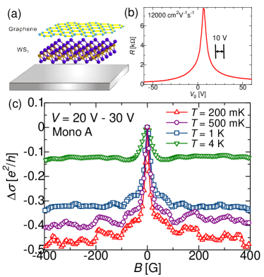
We first show evidence of strong SOIs induced in graphene by a CVD-grown WS2 monolayer. Among different TMDs, WS2 has stronger SOIs compared with Mo-based TMDs [14]. To induce strong SOIs in graphene by WS2, we fabricate heterostructures as schematically shown in Fig. 1(a). In this structure, monolayer graphene is deposited on monolayer CVD-grown WS2.
Since WS2 is a semiconductor and much more resistive than graphene, electronic transport is dominated by graphene in the heterostructures especially at low temperatures. Figure 1(b) displays the resistance as a function of the gate voltage () obtained from graphene on monolayer WS2. The sharp Dirac peak is observed between 0 V and 10 V, demonstrating that the transport is dominated by graphene.
For evaluating the induced SOI in graphene, we employ magnetotransport measurements with magnetic fields perpendicular to the graphene plane. At low temperatures, the phase coherence of the electron’s wave function increases, leading to quantum corrections to the classical Drude conductance for a diffusive conductor. In particular, constructive interferences along time-reversed loops give rise to a low temperature decrease of the conductance. This phenomenon is known as weak localization [18]. This weak localization correction is canceled in a magnetic field which breaks time-reversal symmetry. Therefore one can measure a resistance decrease with magnetic field, over a characteristic scale corresponding to a flux quantum through the square of the phase coherence length. When the system has strong SOIs, however, the situation is different. SOIs give rise to an additional phase (Berry phase) due to the spin rotation of the electronic wave-functions along time-reversed loops. Therefore wave functions interfere destructively, yielding a positive quantum correction to the conductance in zero field and a positive magnetoresistance. This is called weak antilocalization (WAL). Thus by analyzing magnetoresistance data at low temperatures around the zero magnetic field, we can estimate the amplitude of SOIs in the system based on the weak (anti)localization theory [18].
We note that WL in graphene is different from that of the typical 2D electron gas. Because of the valley degree of freedom in graphene, graphene has an additional degree of freedom, chirality. Due to the chirality, if one considers a closed trajectory of an electron localized at one valley in the momentum space, the electron acquires a phase during the itinerary even without SOIs, thus naturally exhibit WAL. This is the origin of the absence of localization for Dirac fermions as observed in topological insulators [19, 20], but for real experimental samples of graphene measured at low temperatures, we usually measure WL rather than WAL [21]. This is because intervalley scatterings due to disorder in real samples easily break the conservation of chirality and suppress WAL. Therefore WAL in graphene is driven solely by SOIs at low temperatures.
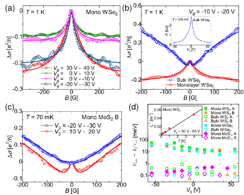
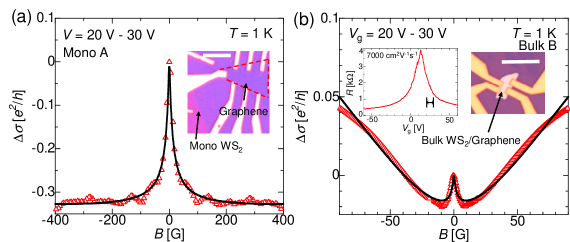
Figure 1(c) shows the quantum conductivity correction () as a function of a perpendicular magnetic field () taken from a sample with graphene/monolayer WS2 (Mono A) at different temperatures in the electron-doped regime. To suppress the effect of universal conductance fluctuation (UCF), whose amplitude is of the same order of magnitude of (), we average 50 curves with different values of gate voltage in a 10 V window around a given . A sharp peak is observed at = 0 and decreases with at all temperatures, indicating that the system is in the WAL regime. In previous reports on magnetotransport for pristine graphene, exhibits WL at low temperatures, thus our results of the observation of WAL demonstrate that the strong SOI is induced in graphene on monolayer WS2. We also fabricate and measure graphene/bulk WS2 (Bulk WS2) samples. Figure 2(a) and (b) are a direct comparison between a Mono WS2 and Bulk WS2 sample in the similar electron-doped region. Both of them exhibit a peak around = 0, a signature of WAL. Interestingly, we also find that magnetoconductivity curves at higher for Mono WS2 becomes extremely flat. The field dependence in this region is determined by the competition between the WL and WAL effects with a characteristic upturn if WL is dominant. Thus the weak dependence at large field indicates that the SOIs induced in graphene by a monolayer WS2 is strong, whereas it is modererate for the case of a WS2 bulk where a sizable upturn is observed.
To evaluate the amplitude of the SOIs precisely, we employ the theoretical formula derived for weak antilocalization in graphene [22]. In this formula, contributions from SOIs enter via relaxation times, and , where sym (asy) denotes the symmetric (asymmetric) contribution to the SO scattering time with respect to the mirror reflection on the graphene plane.
The quantum conductivity correction is expressed as:
| (1) |
where , with the digamma function and . is the phase relaxation time, and . The fits yield three parameters , and . determines the total amplitude of SOI in the system, whereas from the ratio one can evaluate the symmetry type of SOI.
As shown in Fig. 2(a) as an example, all experimental data are reproduced well by using the equation (1). When focused on the total amplitude of the SOI, these fits provide = 0.05 ps, independent of temperature. We note that = 43 ps at 1 K. If we simply define the spin-orbit energy as , we obtain = 13 meV. This value is three orders of magnitude larger than that of pristine graphene [5]. We note that due to the flat tail of at high fields, 0.05 ps provides almost the same curve. Namely, the estimated value of shown above is a lower bound of .
From the difference in the slope of at high fields in Fig. 2(a) and 2(b), we can deduce that the induced SOIs seem smaller in Bulk WS2 than Mono WS2, as already mentioned. To estimate the amplitudes of SOIs in Bulk WS2 more accurately, we also fit the experimental data taken from Bulk WS2 using equation (1). The fits yield = 36 ps and = 4 ps, equivalent to = 170 eV. This value is still larger than that of pristine graphene, but much smaller than that obtained by using monolayer WS2. Therefore monolayer WS2 can induce stronger SOIs in graphene than bulk WS2. The difference in the efficiency to induce strong SOIs between monolayer and bulk TMDs will be discussed in detail in the next section.
4 SOIs in graphene induced by different TMDs with different thickness
To confirm that TMDs can universally induce strong SOIs in graphene, we measure graphene/TMD heterostructures with different types of TMDs with different thickness. In our study we focus on semiconducting 2- structure TMDs, specifically WS2, WSe2 and MoS2. As already shown in the previous section, WS2 can induce strong SOIs in graphene through the proximity effect. Therefore it is also interesting to use WSe2 to induce strong SOIs in graphene since tungsten-based TMDs such as WS2 and WSe2 are reported to have stronger SOI than molybdenum-based SOIs, and also WSe2 has stronger intrinsic SOI than WS2 [14]. Recent theoretical calculations reveal that for the valence band the SOI is 460 meV for monolayer WSe2 while it is 430 meV for monolayer WS2 [14]. Therefore stronger SOIs are expected to be induced in graphene by monolayer WSe2.
We fabricate graphene/monolayer WSe2 (Mono WSe2) and graphene/bulk WSe2 (Bulk WSe2) and estimate SOIs induced in graphene via weak (anti)localization measurements. Figure 3(a) shows obtained from Mono WSe2 at different gate voltages. All curves exihibit WAL peaks, demonstrating that strong SOIs are induced in graphene. Similar to the graphene/WS2 samples, we can also compare the amplitudes of the SOIs induced in graphene by monolayer and bulk WSe2 flakes. Figure 3(b) is a direct comparison between the two curves from the Mono WSe2 and Bulk WSe2 samples. While there is a striking upturn at high fields for Bulk WSe2, a higher peak around = 0 and a flat tail are observed for Mono WSe2. This is in agreement with our previous observations on graphene/WS2 structures and confirms that monolayer TMDs can induce stronger SOIs in graphene than bulk TMDs can.
We also expand our study to evaluate SOIs induced in graphene by molybdenum-based TMD (MoS2). Because the atomic number of molybdenum is smaller than that of tungsten, its intrinsic SOI is also smaller and recent theoretical calculations reported 150 meV for the value of the intrinsic SOI in the valence bands of monolayer MoS2, almost three times smaller than those of the tungsten-based TMDs [14]. Nevertheless, MoS2 is still usable to enhance SOIs in graphene. In Fig. 3(c) from graphene/monolayer MoS2 (Mono MoS2) is plotted both for the electron-doped and hole-doped regions. Especially in the electron-doped region, a clear WAL peak is visible around = 0, a signature of the strong SOIs in graphene. By contrast, the peak in the hole-doped region is weak.
for graphene with different TMDs with different thickness is summarized in Fig. 3(d) for different gate voltages. It reveals that monolayer tungsten-based TMDs (WS2 and WSe2) can induce the strongest SOIs in graphene, and that their bulk counterparts induce weaker SOIs. We find that the amplitude of the SOIs induced by a monolayer MoS2 is comparable to those induced by bulk WS2 and WSe2. Also, the gate dependence of the induced SOI is found to be rather weak. We note that in the hole-doped region for Mono WS2 and Mono WSe2 samples, temperature-independent background signals are superimposed on the WAL signals. Since WL and WAL are quantum effects and temperature dependent, we subtract those temperature-independent backgrounds when we carry out fits based on equation (1) [23, 24].
While it seems reasonable that the SOIs generated by tungsten-based TMDs should be stronger than those induced by molybdenum-based TMDs, the difference between monolayer and bulk TMDs is more difficult to understand in terms of the capacity to induce SOIs in graphene .
There are several differences between monolayer and bulk TMDs. For instance, TMDs such as WS2, WSe2 and MoS2 are in the trigonal-prismatic 2- structure. In the monolayer form, this structure is inversion asymmetric, but in the bulk form, it is inversion symmetric since two neighboring layers are coupled by inversion symmetry. This difference with respect to space inversion operation between monolayer and bulk TMDs is reflected in the band structure of each system. For monolayer TMDs, the bands are spin-split due to the inversion symmetry breaking, whereas they are spin degenerate for bulk TMDs [14, 25, 26]. Recent theoretical studies point out that the strength of the spin splitting in the band structure severely affects the amplitude of SOIs induced in graphene [27]. Therefore monolayer TMDs, which have spin-split bands, are superior to bulk TMDs to generate stronger SOIs in graphene.
Another factor to consider is the possible interface mismatch between bulk TMD crystals and graphene. As reported previously, graphene in real samples is not ideally flat and includes ripples and bubbles. Monolayer TMDs are more flexible so that they can conform to the neighboring graphene layer, but it is more difficult in the case of bulk TMDs. This interface mismatch may reduce the interaction potential between conduction electrons in graphene and atomic orbitals in the TMD. There are no supporting theoretical scenarii for this difference at the time of writing, thus further experimental and theoretical studies are required.
5 Identification of the dominant type of SOIs
In the previous sections, we evaluated the amplitude of SOIs induced in graphene by the TMDs from obtained from the fits based on (1). Three different types of SOIs are theoretically predicted to be induced in graphene on TMDs; Kane-Mele (KM, or intrinsic), Rashba and Valley-Zeeman (VZ) SOI. KM SOI is the intrinsic SOI, thus it exists even in pristine graphene. Rashba SOI is allowed in a system with broken inversion symmetry, especially when the symmetry is broken in the case of 2D materials. Therefore large Rashba SOI may be expected in monolayer graphene on TMD intuitively, but surprisingly it is almost negligible as we will discuss below. In contrast to monolayer graphene, Rashba SOI may be dominant in the case of bilayer graphene on TMD as reported in [28]. On the other hand, VZ SOI breaks A-B sublattice symmetry, and it becomes significant when heavy elements (such as Mo or W) contribute to the sublattice symmetry breaking [29]. By evaluating the ratio between and () in the fits based on the equation (1), we can determine the symmetry of the SOI principally induced in graphene by the TMDs. For all investigated samples, this ratio is found to be larger than 10, which indicates that the Rashba component of the SOIs acting on the in-plane spin components leading to the scattering time is much weaker than the out-of-plane components, which determine the scattering time. For graphene on TMDs, two types of symmetric SOI may be considered, the intrinsic KM SOI and VZ SOI. The former and the latter are respectively symmetric and asymmetric about the A-B symmetry of the hexagonal lattice. We note that the lattice parameters of TMDs and graphene are different. Moreover, we do not specifically align the relative orientations of the two layers. Therefore it is a priori tempting to assume that carriers in graphene are scattered randomly by heavy TMD atoms. However, it is shown theoretically [27, 30] that this is not an appropriate picture and that in spite of the incommensurablity between the two lattices , the TMD/graphene bilayer retains a symmetry whereas the initial of Graphene is lost. Actually a VZ SOI is induced in graphene with an amplitude of a few meV depending on the nature of the TMD. In the following we show that our experimental data are consistent with these findings.
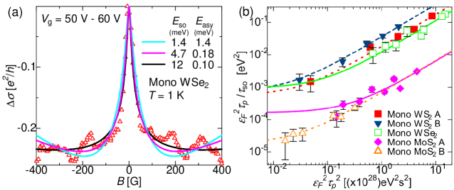
Figure 4(a) shows fits for the Mono WSe2 sample with different ratios between and . The fits with unambiguously give a much better description of the experimental results. This demonstrates that the symmetry of the SOIs induced in graphene by the TMDs is predominantly symmetric.
| Sample | [meV] | [meV] |
| Mono WSe2 | 48.0 12.2 | 3.3 0.10 |
| Mono WS2 A | 27.4 2.8 | 4.4 0.047 |
| Mono WS2 B | 32.9 3.8 | 6.4 0.14 |
| Mono MoS2 A | 10.3 1.7 | 0.87 0.035 |
| Mono MoS2 B | 4.3 0.035 | 0.86 3.5 |
| Bulk WSe2 | 11.6 2.1 | 0.38 0.013 |
| Bulk WS2 A | 8.9 3.7 | 0.73 0.028 |
| Bulk WS2 B | - | 0.72 0.022 |
We first note that the KM and VZ SOI, both of which are symmetric, give rise to different spin relaxation mechanisms in graphene. There are two spin relaxation mechanisms in graphene, Elliot-Yafet (EY) and D’yakonov-Pérel (DP). These two mechanisms provide different dependences of on , where is the momentum relaxation time. Whereas for the EY mechanism, for the DP. The KM SOI contributes to the EY spin relaxation mechanism since the DP mechanism requires spin-splitting due to inversion symmetry breaking. On the other hand, since the VZ SOI originates from broken sublattice symmetry, it leads to a DP-type spin relaxation. We neglect the smaller contributions from the Rashba SOI . Each contribution (EY or DP) can be determined by fitting the relation between and the momentum relaxation time following the equation [31]:
| (2) |
where is the amplitude of spin-orbit coupling leading to the EY (DP) mechanism and is the Fermi energy. Figure 4(b) displays the relation in equation (2) for each sample. It is clear from these expressions that the DP scattering mechanism is dominant in the highly doped region whereas the EY is dominant in the vicinity of the Dirac point. In Table 1, we show the fitting parameters and obtained from the fits for each device. The DP energy scales found are in good agreement with theoretical predictions concerning the VZ SOI [30]. We also find a large EY contribution whose origin is more difficult to explain since the KM intrinsic SO contribution is expected to be small compared to the VZ one, considering the recent theoretical studies [27, 30]. Up to now we do not have a good explanation for these large values of . However we must note that these values are extracted from data taken close to the Dirac point where the formation of a disordered network of electron-hole puddles dominates the properties of graphene [32] and is ill-defined, resulting in possible important errors in the determination of from (2).
6 Superconducting Josephson junctions with graphene/WS2 heterostructures
Now that we have confirmed that strong SOIs can be induced in graphene by the TMDs, it is also tempting to integrate graphene/TMD heterostructures into superconducting Josephson junctions. There have already been many studies on Josephson junctions with graphene [33, 34, 35, 36, 37], but transport properties of supercurrent in graphene with strong SOIs have never been explored. SOIs are an essential ingredient to realize topological superconductivity, thus it is of great significance to investigate effects of strong SOIs on supercurrent transport in graphene. In this section, we present robust supercurrent observed in Josephson junctions with graphene/WS2 heterostructures.
The device structure is illustrated in Fig. 5(a). In this study we employ superconducting electrodes made of MoRe because it provides a good superconducting contact to graphene without any buffer layers, and possesses high critical temperature ( 10 K) and high critical magnetic field ( 8 T). The MoRe electrodes are connected to two types of structures, either hBN/graphene/WS2 (Gr/WS2) or hBN/graphene/hBN (Gr/hBN) heterostrucures, forming a superconducting Josephson junction. The width of graphene is around 10 m for all junctions, and the length of the junction ranges from 100 nm to 500 nm, depending on the sample.
We first show the gate dependence of the resistance in Fig. 5(b). There is a striking difference between Gr/WS2 and Gr/hBN junctions, and the Dirac peak for the Gr/WS2 junction is much broader than that of the Gr/hBN junction. This indicates that the mobility of graphene on WS2 is much smaller than that on hBN. While a recent study reported that TMDs can be a substrate as good as hBN for graphene [38], since our samples employ monolayer CVD-grown WS2, the surface of flakes is not as flat as multilayer hBN, and also there may remain some residues on the surface, originating from the transfer process of CVD-grown WS2 from the original substrate used during the growth to a fresh substrate for measurements (see Section 2). We note that all Gr/WS2 junctions with different have a lower mobility than the Gr/hBN junctions with the same . For = 100 nm and 200 nm Gr/hBN junctions, we observe Fabry-Pérot-like oscillations in the hole doped region (not shown) in the normal state. This is in agreement with previous reports [36, 35], and demonstrates that these two junctions are in the ballistic regime.
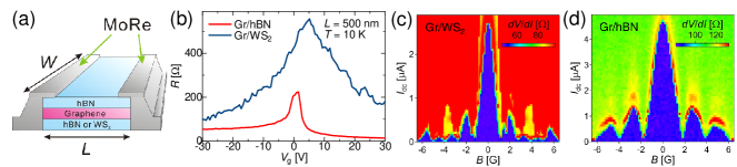
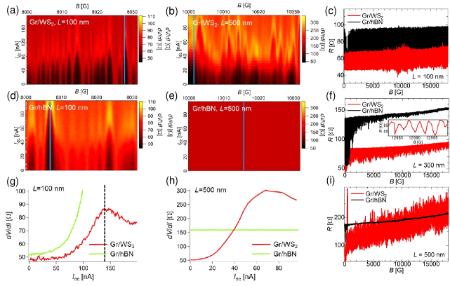
Figure 5(c) and (d) display the differential resistance () as a function of magnetic field () for = 500 nm Gr/WS2 (c) and Gr/hBN (d) junctions. To measure , a small ac current () is added to the dc current (). Fraunhofer-like oscillations are clearly observed, a signature of supercurrent flowing through the junctions. Slight deviations from the ideal shape of oscillations may be due to small inhomogeneities of the current distribution in the junction. The Gr/hBN sample exhibits larger critical current () at zero field, consistent with the higher mobility of graphene.
While superconducting properties are better for Gr/hBN junctions than Gr/WS2 around the zero field, these characters become dramatically different at higher fields. Figure 6 displays around 1 T (10000 G). For = 100 nm junctions, even around 8000 G, dips are observed in and oscillates with for both junctions (Fig. 6(a) and (d)). In the previous report on graphene ballistic Josephson junctions, field-dependent and sample-specific differential resistance dips at a low current were also observed around 5000 G, and the and regions of low were termed ’superconducting pockets’ [35]. In our shortest samples, the superconducting pockets are still visible around = 16000 G for the Gr/WS2 junction (not shown). We note that all Gr/WS2 junctions, even the shortest one with = 100 nm, are in the diffusive limit due to the shorter mean free path , whereas the = 100 nm Gr/hBN junction is in the ballistic limit.
While signatures of robust supercurrent are observed for both Gr/hBN and Gr/WS2 junctions for = 100 nm samples, a striking difference emerges for longer junctions ( = 500 nm). Figure 6 (b) and (e) display the colour-coded differential resistance as a function of and , for around 10000 G for Gr/WS2 ((b)) and Gr/hBN ((e)) junctions. For the Gr/WS2 junction superconducting pockets are still observable. By contrast, they are completely suppressed for Gr/hBN junctions. In Fig. 6 (g) and (h) we compare crosssectional cuts of for both samples with =100 nm ((g)) and = 500 nm ((h)). The suppressed (Gr/WS2) and flat (Gr/hBN) are shown more explicitly in Fig 6(h).
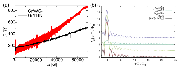
To investigate the evolution of in a broader range of field, we measure the zero bias differential resistance () with increasing field. Figure 6 (c), (f) and (i) show the relation between and for = 100 nm ((c)), = 500 nm ((i)) and also for = 300 nm ((f)) Gr/WS2 and Gr/hBN junctions. For the = 100 nm junctions, the amplitudes of oscillations are comparable for both Gr/WS2 and Gr/hBN junctions up to 18000 G. However, for the = 300 nm junctions, while the Gr/WS2 junction exhibits relatively large amplitude of oscillations even around = 18000 G, the amplitude is strongly suppressed for the Gr/hBN junction. The difference is much more striking for the = 500 nm junctions. Whereas the oscillations are rapidly suppressed for less than 1000 G for the Gr/hBN junction, continuously oscillates up to 18000 G for the Gr/WS2 junction. We show that the oscillations are still observable even at 70000 G in Fig. 7(a) [39].
Now we discuss the possible origin of superconducting pockets for these junctions. As for = 100 nm ballistic Gr/hBN junctions, Andreev bound states mediated by chaotic ballistic billiard paths located at the edges of graphene have already been proposed as an origin [35]. Those chaotic paths can be regarded as a ballistic analog of the quasi-classical phase-coherent paths and produce mesoscopic fluctuations of the supercurrent . In the case of ballistic short junctions, is estimated as
| (3) |
where denotes the superconducting gap at = 0 [40].
This formula yields 240 nA for short Gr/hBN junctions, slightly higher than the experimentally observed value. We note that the above formula is calculated in the zero field limit. For finite magnetic fields, a recent theoretical study for 2D ballistic junctions provides a picture of supercurrent distribution at high fields [41]. As increases, supercurrent is localized close to the edges, and decays faster () than the typical decay of around the zero field (). By contrast, supercurrent fluctuations persists even at high fields, and are expressed as with . This estimate provides 200 nA for the = 100 nm Gr/hBN ballistic junctions, in qualitative agreement with our experimental results. However, these high field supercurrent fluctuations are specific for ballistic junctions, and not expected for diffusive junctions.
In order to explain the robust supercurrent signatures which we find in the diffusive Gr/WS2 junctions, it thus seems necessary to account for the role of SOIs. SOIs favor the formation of edge states, epitomized by the topological quantum spin Hall phase [42]. We note that it is unlikely for our results to be relevant to the topological edge states because our measurements are carried out in the highly-doped region. On the other hand, edge states can also exist in a non-topological system, and coexist with bulk states of the same energy [43]. Such edge states are generally sensitive to scattering, but some degree of protection against smooth disorder may exist if the edge states are well separated from bulk states in momentum space. In addition, spin can also provide additional protection if the spins of the edge state and those of the nearby bulk band are opposite. In the case of graphene on WS2, the analysis of weak antilocalization experiments, see previous sections and [23, 24, 44, 28, 45], has shown that the induced SOIs have both a Rashba-type in-plane component and a more than ten-folds larger out-of-plane component, predominantly of valley-Zeeman type probably. The combined effect of those two types of interactions was demonstrated theoretically to generate non-topological edge states along zigzag edges [46]. For exploring whether such edge states may explain the persistance and oscillations of supercurrent at high fields, we have carried out simulations of as a function of in graphene strips containing different types of SOIs (Fig. 7(b)). We find that supercurrent persists up to higher fields with SOIs than that without SOIs, even when disorder is included. Due to divergently increasing calculational time with increasing number of the flux quanta, we unfortunatly cannot reach the regime where thousands of flux quanta thread the junction. Further theoretical studies are awaited.
While we carried out our supercurrent experiments in the highly doped region, it may be interesting to contemplate the properties of the edge state from the view point of topological physics. Nontopological edge states are theoretically predicted as shown in [46], but no theoretical works address the graphene VZ SOI system proximitized by superconductivity. As evidenced in previous studies, supercurrent transport reveals topological properties of the system [47, 48, 49]. Considering the fact that the edge states observed in our study are protected against disorder, novel topological phases are possible. Theoretical works such as Majorana fermions in a half-metallic wire on an Ising superconductor [50] may be helpful to obtain some insights to study these novel phases.
We comment on the relation between those edge paths and the chiral edge states of the quantum Hall (QH) regime. The QH regime develops when the mean free path , where is the cycrotron radius () [33]. For example at = 60 V and = 10000 G, 500 nm, thus chiral edge states do not contribute to the Andreev bound states localized at the edge. We note that this 2 value is much larger than = 30 nm of = 500 nm Gr/WS2 junction. At higher fields, becomes smaller than , so that the Landau localization of bulk states and the formation of chiral edge states may become relevant. We observe superconducting pockets even at 70000 G for Gr/WS2 junction for = 500 nm, and 30 nA [39]. However, this value is more than one order of magnitude larger than reported in the QH regime with a comparable for shorter and narrower junctions with better quality graphene [33]. This may indicate that the supercurrent enhancement by the SOIs can also be effective in the QH regime.
7 Discussions and future possibilities
In this review we showed that strong SOIs can be induced in graphene through heterostructures with TMDs. The susceptibility of graphene’s exposed 2D electron gas facilitates the modulation of its transport properties via proximity effects. Owing to interactions between electrons in graphene and - or -orbitals in TMDs, originating from calchogen and heavy atom, respectively, the strong intrinsic SOI in TMDs are transferred to graphene, thereby WAL signals are observed in magneto-transport measurements at low temperatures. While all of the TMDs have stronger SOIs than graphene, monolayer tungsten-based TMDs (WS2 and WSe2) bring considerable enhancement of SOIs in graphene compared with their bulk counterparts or other TMDs.
In addition to the normal-state transport properties, supercurrent transport through graphene exhibits dramatic changes driven by the strong SOIs. Even for diffusive graphene with relatively low mobility, signatures of robust supercurrent are observed even around 1 T in Gr/WS2 Josephson junctions. Specifically, for the =500 nm Gr/WS2 junctions, dips of the differential resistance are observed in magnetic fields as high as 7 T, a signature of superconductivity induced in graphene. These exotic phemena may be driven by the localization of supercurrent near the edges protected by the strong SOIs.
While it is clear that graphene/TMD hybrid structures are an intriguing system to explore, several issues still remain to be clarified. This system has been investigated both theoretically and experimentally, but there are discrepancies in the estimates of the induced SOIs in graphene. Early theoretical reports based on the DFT calculations predict SOI amplitudes of the order of 1 meV [51, 52], smaller than the values obtained in experiments [23, 24, 53, 45, 54, 55, 44, 28, 56, 57]. More recently, the angular dependence of the SOIs induced in graphene by the TMDs has been considered [27, 30]. These studies take into account a finite angle between graphene and a TMD layer, more appropriate to real experimental devices. They demonstrate that the amplitudes of the SOIs induced in graphene dramatically change depending on the relative angle between the two layers, and at certain angles the SOIs become a few tens of meV, much larger than the values estimated based on the DFT calculations where the relative angle between the two layers is always set to zero. The discrepancies between the theoretical estimates and experimental ones may also be due to differences in the position of the Fermi level in the band structure of the system. For graphene/TMD bilayers, the band structure is generically the superposition of the band structure of graphene and the TMD. However, the position of the Dirac cone (note that now the linear band crossing is gapped due to the SOIs and bands are spin-split) depends on the combination of graphene and the TMD. It is shown that the amplitudes of the induced SOIs are highly affected by the position of the Fermi level in the band structure [30]. The band structure of graphene/TMD hybrids has been experimentally investigated by angular-resolved spectroscopy (ARPES) measurements [58, 59]. In the case of graphene/MoS2 heterostructures, while the ARPES data show that the Fermi level is located around the middle of the conduction band, the DFT calculations propose that the Fermi level is near the conduction band edge of MoS2 [51, 58]. This discrepancy between the experimental results and calculations may also be one of the reasons for the difference between the theoretical and experimental estimates of the SOIs. To clarify these points further systematic experimental studies are essential including different experimental probes. One of the promising candidates among them is resistively-detected electron-spin resonance (RD ESR) technique, already used to determine the amplitude of the intrinsic SOI in graphene [60, 61]. By using this technique it may be possible to reveal the band structure of graphene/TMD hybrids, thereby more precise values of SOIs can be extracted.
We now briefly discuss future directions of the graphene/TMD hybrid system. As for normal state transport phenomena, since it is possible to generate spin currents even without ferromagnetic contacts by using nonmagnetic TMDs such as MoS2 or WSe2, it is of great interest to fabricate a device with pristine graphene connected to graphene/TMD electrodes. These electrodes act as a spin current generator and detector. So far there have been reports on spin transport in a graphene/TMD bilayer [62, 63, 64, 65]. However, ferromagnetic metals are exploited as a spin injector or detector in these studies. By using a graphene/TMD bilayer as a spin injector and detector for ”pristine” graphene instead of conventional ferromagnetic electrodes, it becomes much easier to overcome spin impedance mismatch problem between spin injector/detector and graphene. By depositing TMD flakes partially on graphene, it is realizable to make such a device.
It is also attractive to explore supercurrent properties in graphene/TMD Josephson junctions. To demonstrate more explicitly the localization of supercurrent, scanning tunneling microscope (STM) may be useful to show the edge states which carry supercurrent. Since supercurrent can flow for as long as 500 nm in graphene/WS2 Josephson junctions, it is also possible to fabricate more complex structures to carry out further investigations of supercurrent transport.
8 Acknowledgement
Our studies presented here were realized in collaboration with C. Mattevi, M. Och, P. Palczynski, F. Reale, T. Taniguchi, K. Watanabe, A. D. Chepelianskii, M. Ferrier, N. J. Wu, M. Q. Zhao, A. T. C. Johnson and A. Ouerghi. We sincerely acknowledge strong supports by our cowokers. Our projects are finantially supported in part by the Marie Sklodowska Curie Individual Fellowships (H2020-MSCAIF-2014-659420); the ANR Grants DIRACFORMAG (ANR-14-CE32-003), MAGMA(ANR-16-CE29-0027-02), and JETS (ANR-16-CE30-0029-01); the Overseas Research Fellowships by the Japan Society for the Promotion of Science (2017-684); and the CNRS. K. W. and T. T. acknowledge support from the Elemental Strategy Initiative conducted by the MEXT, Japan, Grant No. JPMXP0112101001, JSPS KAKENHI Grant No. JP20H00354, and the CREST (JPMJCR15F3), JST. \printcredits
References
- [1] K. S. Novoselov, A. K. Geim, S. V. Morozov, D. Jiang, Y. Zhang, S. V. Dubonos, I. V. Grigorieva, A. A. Firsov, Electric field effect in atomically thin carbon films, Science 306 (2004) 666–669.
- [2] Y. Cao, V. Fatemi, S. Fang, K. Watanabe, T. Taniguchi, E. Kaxiras, P. Jarillo-Herrero, Unconventional superconductivity in magic-angle graphene superlattices, Nature 556 (2018) 43–50.
- [3] M. I. Katsnelson, K. S. Novoselov, A. K. Geim, Chiral tunnelling and the Klein paradox in graphene, Nature Physics 2 (2006) 620–625.
- [4] Y. Barlas, K. Yang, A. H. MacDonald, Quantum Hall effects in graphene-based two-dimensional electron systems, Nanotechnology 23 (2012) 052001.
- [5] M. Gmitra, S. Konschuh, C. Ertler, C. Ambrosch-Draxl, J. Fabian, Band-structure topologies of graphene: Spin-orbit coupling effects from first principles, Phys. Rev. B 80 (2009) 235431.
- [6] I. Žutić, J. Fabian, S. Das Sarma, Spintronics: Fundamentals and applications, Rev. Mod. Phys. 76 (2004) 323–410.
- [7] M. Z. Hasan, C. L. Kane, Colloquium: Topological insulators, Rev. Mod. Phys. 82 (2010) 3045–3067.
- [8] C. Weeks, J. Hu, J. Alicea, M. Franz, R. Wu, Engineering a robust quantum spin Hall state in graphene via adatom deposition, Phys. Rev. X 1 (2011) 021001.
- [9] J. Hu, J. Alicea, R. Wu, M. Franz, Giant topological insulator gap in graphene with 5d adatoms, Phys. Rev. Lett. 109 (2012) 266801.
- [10] J. Balakrishnan, G. K. W. Koon, A. Avsar, Y. Ho, J. H. Lee, M. Jaiswal, S.-J. Baeck, J.-H. Ahn, A. Ferreira, M. A. Cazalilla, A. H. C. Neto, B. ’́Ozyilmaz, Giant spin Hall effect in graphene grown by chemical vapour deposition, Nature Communications 5 (2014) 4748.
- [11] C. R. Dean, A. F. Young, I. Meric, C. Lee, L. Wang, S. Sorgenfrei, K. Watanabe, T. Taniguchi, P. Kim, K. L. Shepard, J. Hone, Boron nitride substrates for high-quality graphene electronics, Nature Nanotechnology 5 (2010) 722–726.
- [12] L. Wang, I. Meric, P. Y. Huang, Q. Gao, Y. Gao, H. Tran, T. Taniguchi, K. Watanabe, L. M. Campos, D. A. Muller, J. Guo, P. Kim, J. Hone, K. L. Shepard, C. R. Dean, One-dimensional electrical contact to a two-dimensional material, Science 342 (2013) 614–617.
- [13] Z. Wang, C. Tang, R. Sachs, Y. Barlas, J. Shi, Proximity-induced ferromagnetism in graphene revealed by the anomalous Hall effect, Phys. Rev. Lett. 114 (2015) 016603.
- [14] D. Xiao, G.-B. Liu, W. Feng, X. Xu, W. Yao, Coupled spin and valley physics in monolayers of MoS2 and other group-VI dichalcogenides, Phys. Rev. Lett. 108 (2012) 196802.
- [15] A. Splendiani, L. Sun, Y. Zhang, T. Li, J. Kim, C.-Y. Chim, G. Galli, F. Wang, Emerging photoluminescence in monolayer MoS2, Nano Letters 10 (2010) 1271–1275.
- [16] K. F. Mak, C. Lee, J. Hone, J. Shan, T. F. Heinz, Atomically thin MoS2: A new direct-gap semiconductor, Phys. Rev. Lett. 105 (2010) 136805.
- [17] F. Reale, P. Palczynski, I. Amit, G. F. Jones, J. D. Mehew, A. Bacon, N. Ni, P. C. Sherrell, S. Agnoli, M. F. Craciun, S. Russo, C. Mattevi, High-mobility and high-optical quality atomically thin WS2, Scientific Reports 7 (2017) 14911.
- [18] G. Bergmann, Weak localization in thin films: A time-of-flight experiment with conduction electrons, Physics Reports 107 (1984) 1 – 58.
- [19] K. Nomura, M. Koshino, S. Ryu, Topological delocalization of two-dimensional massless Dirac fermions, Phys. Rev. Lett. 99 (2007) 146806.
- [20] M. Liu, J. Zhang, C.-Z. Chang, Z. Zhang, X. Feng, K. Li, K. He, L.-l. Wang, X. Chen, X. Dai, Z. Fang, Q.-K. Xue, X. Ma, Y. Wang, Crossover between weak antilocalization and weak localization in a magnetically doped topological insulator, Phys. Rev. Lett. 108 (2012) 036805.
- [21] F. V. Tikhonenko, D. W. Horsell, R. V. Gorbachev, A. K. Savchenko, Weak localization in graphene flakes, Phys. Rev. Lett. 100 (2008) 056802.
- [22] E. McCann, V. I. Fal’ko, z -z symmetry of spin-orbit coupling and weak localization in graphene, Phys. Rev. Lett. 108 (2012) 166606.
- [23] T. Wakamura, F. Reale, P. Palczynski, S. Guéron, C. Mattevi, H. Bouchiat, Strong anisotropic spin-orbit interaction induced in graphene by monolayer WS2, Phys. Rev. Lett. 120 (2018) 106802.
- [24] T. Wakamura, F. Reale, P. Palczynski, M. Q. Zhao, A. T. C. Johnson, S. Guéron, C. Mattevi, A. Ouerghi, H. Bouchiat, Spin-orbit interaction induced in graphene by transition metal dichalcogenides, Phys. Rev. B 99 (2019) 245402.
- [25] J. M. Riley, F. Mazzola, M. Dendzik, M. Michiardi, T. Takayama, L. Bawden, C. Granerod, M. Leandersson, T. Balasubramanian, M. Hoesch, T. K. Kim, H. Takagi, W. Meevasana, P. Hofmann, M. S. Bahramy, J. W. Wells, P. D. C. King, Direct observation of spin-polarized bulk bands in an inversion-symmetric semiconductor, Nature Physics 10 (2014) 835–839.
- [26] D. W. Latzke, W. Zhang, A. Suslu, T.-R. Chang, H. Lin, H.-T. Jeng, S. Tongay, J. Wu, A. Bansil, A. Lanzara, Electronic structure, spin-orbit coupling, and interlayer interaction in bulk MoS2 and WS2, Phys. Rev. B 91 (2015) 235202.
- [27] Y. Li, M. Koshino, Twist-angle dependence of the proximity spin-orbit coupling in graphene on transition-metal dichalcogenides, Phys. Rev. B 99 (2019) 075438.
- [28] Z. Wang, D.-K. Ki, J. Y. Khoo, D. Mauro, H. Berger, L. S. Levitov, A. F. Morpurgo, Origin and magnitude of ’designer’ spin-orbit interaction in graphene on semiconducting transition metal dichalcogenides, Phys. Rev. X 6 (2016) 041020.
- [29] D. Kochan, S. Irmer, J. Fabian, Model spin-orbit coupling hamiltonians for graphene systems, Phys. Rev. B 95 (2017) 165415.
- [30] A. David, P. Rakyta, A. Kormányos, G. Burkard, Induced spin-orbit coupling in twisted graphene–transition metal dichalcogenide heterobilayers: Twistronics meets spintronics, Phys. Rev. B 100 (2019) 085412.
- [31] P. J. Zomer, M. H. D. Guimaraes, N. Tombros, B. J. van Wees, Long-distance spin transport in high-mobility graphene on hexagonal boronnitride, Phys. Rev. B 86 (2012) 161416.
- [32] J. Martin, N. Akerman, G. Ulbricht, T. Lohmann, J. H. Smet, K. von Klitzing, A. Yacoby, Observation of electron–hole puddles in graphene using a scanning single-electron transistor, Nature Physics 4 (2008) 144–148.
- [33] F. Amet, C. T. Ke, I. V. Borzenets, J. Wang, K. Watanabe, T. Taniguchi, R. S. Deacon, M. Yamamoto, Y. Bomze, S. Tarucha, G. Finkelstein, Supercurrent in the quantum Hall regime, Science 352 (2016) 966–969.
- [34] I. V. Borzenets, F. Amet, C. T. Ke, A. W. Draelos, M. T. Wei, A. Seredinski, K. Watanabe, T. Taniguchi, Y. Bomze, M. Yamamoto, S. Tarucha, G. Finkelstein, Ballistic graphene josephson junctions from the short to the long junction regimes, Phys. Rev. Lett. 117 (2016) 237002.
- [35] M. Ben Shalom, M. J. Zhu, V. I. Fal’ko, A. Mishchenko, A. V. Kretinin, K. S. Novoselov, C. R. Woods, K. Watanabe, T. Taniguchi, A. K. Geim, J. R. Prance, Quantum oscillations of the critical current and high-field superconducting proximity in ballistic graphene, Nature Physics 12 (2016) 318–322.
- [36] V. E. Calado, S. Goswami, G. Nanda, M. Diez, A. R. Akhmerov, K. Watanabe, T. Taniguchi, T. M. Klapwijk, L. M. K. Vandersypen, Ballistic Josephson junctions in edge-contacted graphene, Nature Nanotechnology 10 (2015) 761–764.
- [37] L. Zhao, E. G. Arnault, A. Bondarev, A. Seredinski, T. F. Q. Larson, A. W. Draelos, H. Li, K. Watanabe, T. Taniguchi, F. Amet, H. U. Baranger, G. Finkelstein, Interference of chiral andreev edge states, Nature Physics 16 (2020) 862–867.
- [38] J. O. Island, X. Cui, C. Lewandowski, J. Y. Khoo, E. M. Spanton, H. Zhou, D. Rhodes, J. C. Hone, T. Taniguchi, K. Watanabe, L. S. Levitov, M. P. Zaletel, A. F. Young, Spin–orbit-driven band inversion in bilayer graphene by the van der Waals proximity effect, Nature 571 (2019) 85–89.
- [39] T. Wakamura, N. J. Wu, A. D. Chepelianskii, S. Guéron, M. Och, M. Ferrier, T. Taniguchi, K. Watanabe, C. Mattevi, H. Bouchiat, Spin-orbit-enhanced robustness of supercurrent in Graphene/WS2 Josephson junctions, Phys. Rev. Lett. 125 (2020) 266801.
- [40] C. W. J. Beenakker, Universal limit of critical-current fluctuations in mesoscopic Josephson junctions, Phys. Rev. Lett. 67 (1991) 3836–3839.
- [41] H. Meier, V. I. Fal’ko, L. I. Glazman, Edge effects in the magnetic interference pattern of a ballistic SNS junction, Phys. Rev. B 93 (2016) 184506.
- [42] M. König, H. Buhmann, L. W. Molenkamp, T. Hughes, C.-X. Liu, X.-L. Qi, S.-C. Zhang, The quantum spin Hall effect: Theory and experiment, Journal of the Physical Society of Japan 77 (2008) 031007.
- [43] V. P. Ostroukh, B. Baxevanis, A. R. Akhmerov, C. W. J. Beenakker, Two-dimensional josephson vortex lattice and anomalously slow decay of the Fraunhofer oscillations in a ballistic SNS junction with a warped Fermi surface, Phys. Rev. B 94 (2016) 094514.
- [44] Z. Wang, D.-K. Ki, H. Chen, H. Berger, A. H. MacDonald, A. F. Morpurgo, Strong interface-induced spin–orbit interaction in graphene on WS2, Nature Communications 6 (2015) 8339.
- [45] S. Zihlmann, A. W. Cummings, J. H. Garcia, M. Kedves, K. Watanabe, T. Taniguchi, C. Schönenberger, P. Makk, Large spin relaxation anisotropy and valley-Zeeman spin-orbit coupling in WSe2/graphene/h-BN heterostructures, Phys. Rev. B 97 (2018) 075434.
- [46] T. Frank, P. Högl, M. Gmitra, D. Kochan, J. Fabian, Protected pseudohelical edge states in Z2-trivial proximitized graphene, Phys. Rev. Lett. 120 (2018) 156402.
- [47] C. Li, J. C. de Boer, B. de Ronde, S. V. Ramankutty, E. van Heumen, Y. Huang, A. de Visser, A. A. Golubov, M. S. Golden, A. Brinkman, 4-periodic Andreev bound states in a Dirac semimetal, Nature Materials 17 (2018) 875–880.
- [48] A.-Q. Wang, C.-Z. Li, C. Li, Z.-M. Liao, A. Brinkman, D.-P. Yu, 4-periodic supercurrent from surface states in Cd3As2 nanowire-based Josephson junctions, Phys. Rev. Lett. 121 (2018) 237701.
- [49] A. Murani, A. Kasumov, S. Sengupta, Y. A. Kasumov, V. T. Volkov, I. I. Khodos, F. Brisset, R. Delagrange, A. Chepelianskii, R. Deblock, H. Bouchiat, S. Guéron, Ballistic edge states in bismuth nanowires revealed by SQUID interferometry, Nature Communications 8 (2017) 15941.
- [50] B. T. Zhou, N. F. Q. Yuan, H.-L. Jiang, K. T. Law, Ising superconductivity and Majorana fermions in transition-metal dichalcogenides, Phys. Rev. B 93 (2016) 180501.
- [51] M. Gmitra, J. Fabian, Graphene on transition-metal dichalcogenides: A platform for proximity spin-orbit physics and optospintronics, Phys. Rev. B 92 (2015) 155403.
- [52] M. Gmitra, D. Kochan, P. Högl, J. Fabian, Trivial and inverted Dirac bands and the emergence of quantum spin Hall states in graphene on transition-metal dichalcogenides, Phys. Rev. B 93 (2016) 155104.
- [53] A. Avsar, J. Y. Tan, T. Taychatanapat, J. Balakrishnan, G. K. W. Koon, Y. Yeo, J. Lahiri, A. Carvalho, A. S. Rodin, E. C. T. O’Farrell, G. Eda, A. H. Castro Neto, B. Özyilmaz, Spin–orbit proximity effect in graphene, Nature Communications 5 (2014) 4875.
- [54] T. Völkl, T. Rockinger, M. Drienovsky, K. Watanabe, T. Taniguchi, D. Weiss, J. Eroms, Magnetotransport in heterostructures of transition metal dichalcogenides and graphene, Phys. Rev. B 96 (2017) 125405.
- [55] S. Ringer, S. Hartl, M. Rosenauer, T. Völkl, M. Kadur, F. Hopperdietzel, D. Weiss, J. Eroms, Measuring anisotropic spin relaxation in graphene, Phys. Rev. B 97 (2018) 205439.
- [56] B. Yang, M.-F. Tu, J. Kim, Y. Wu, H. Wang, J. Alicea, R. Wu, M. Bockrath, J. Shi, Tunable spin–orbit coupling and symmetry-protected edge states in graphene/WS2, 2D Materials 3 (2016) 031012.
- [57] B. Yang, M. Lohmann, D. Barroso, I. Liao, Z. Lin, Y. Liu, L. Bartels, K. Watanabe, T. Taniguchi, J. Shi, Strong electron-hole symmetric Rashba spin-orbit coupling in graphene/monolayer transition metal dichalcogenide heterostructures, Phys. Rev. B 96 (2017) 041409.
- [58] D. Pierucci, H. Henck, J. Avila, A. Balan, C. H. Naylor, G. Patriarche, Y. J. Dappe, M. G. Silly, F. Sirotti, A. T. C. Johnson, M. C. Asensio, A. Ouerghi, Band alignment and minigaps in monolayer MoS2-graphene van der Waals heterostructures, Nano Letters 16 (2016) 4054–4061.
- [59] H. Henck, Z. Ben Aziza, D. Pierucci, F. Laourine, F. Reale, P. Palczynski, J. Chaste, M. G. Silly, F. m. c. Bertran, P. Le Fèvre, E. Lhuillier, T. Wakamura, C. Mattevi, J. E. Rault, M. Calandra, A. Ouerghi, Electronic band structure of two-dimensional WS2/graphene van der Waals heterostructures, Phys. Rev. B 97 (2018) 155421.
- [60] J. Sichau, M. Prada, T. Anlauf, T. J. Lyon, B. Bosnjak, L. Tiemann, R. H. Blick, Resonance microwave measurements of an intrinsic spin-orbit coupling gap in graphene: A possible indication of a topological state, Phys. Rev. Lett. 122 (2019) 046403.
- [61] C. H. Sharma, P. Zhao, L. Tiemann, M. Prada, A. D. Pandey, A. Stierle and R. H. Blick, Electron-Spin-Resonance in a proximity-coupled MoS2/Graphene van-der-Waals heterostructure, arXiv:2111.00530.
- [62] S. Omar, B. J. van Wees., Spin transport in high-mobility graphene on WS2 substrate with electric-field tunable proximity spin-orbit interaction, Phys. Rev. B 97 (2018) 045414.
- [63] L. A. Benítez, J. F. Sierra, W. Savero Torres, A. Arrighi, F. Bonell, M. V. Costache, S. O. Valenzuela, Strongly anisotropic spin relaxation in graphene–transition metal dichalcogenide heterostructures at room temperature, Nature Physics 14 (2018) 303–308.
- [64] T. S. Ghiasi, A. A. Kaverzin, P. J. Blah, B. J. van Wees, Charge-to-spin conversion by the Rashba–Edelstein effect in two-dimensional van der Waals heterostructures up to room temperature, Nano Letters 19 (2019) 5959–5966.
- [65] L. A. Benítez, W. Savero Torres, J. F. Sierra, M. Timmermans, J. H. Garcia, S. Roche, M. V. Costache, S. O. Valenzuela, Tunable room-temperature spin galvanic and spin Hall effects in van der Waals heterostructures, Nature Materials 19 (2020) 170–175.