Combining one and two photon polymerization for accelerated high performance (3+1)D photonic integration
Abstract
Dense and efficient circuits with component sizes approaching the physical limit is the hallmark of high performance integration. Ultimately, these features and their pursuit enabled the multi-decade lasting exponential growth of components on integrated electronic chips according to Moore’s law, which culminated with the high performance electronics we know today. However, current fabrication technology is mostly constraint to 2D lithography, and thermal energy dissipation induced by switching electronic signal lines presents a fundamental challenge for truly 3D electronic integration. Photonics reduces this problem, and 3D photonic integration is therefore a highly sought after technology that strongly gains in relevance due to the need for scalable application-specific integrated circuits for neural networks. Direct laser writing of a photoresin is a promising high-resolution tool for 3D photonic integration. Here, we combine one and two-photon polymerization (TPP) for waveguide integration for the first time, dramatically accelerating the fabrication process and increasing optical confinement. 3D additive printing is based on femtosecond TPP, while blanket irradiation with a UV lamp induces one-photon polymerization (OPP) throughout the entire 3D chip. We locally and dynamically adjust writing conditions to implement (3+1)D flash-TPP: waveguide cores are printed with a small distance between neighboring writing voxels to ensure smooth interfaces, mechanical support structures are printed at maximal distance between the voxels to speed up the process. Finally, the entire chip’s passive volume not part of waveguide cores or mechanical support is polymerized in a single instance by UV blanket irradiation. This decouples fabrication time from the passive volume’s size. We succeed in printing vertical single-mode waveguides of 6 mm length that reach up to NA = 0.16. Noteworthy, we achieve exceptionally low -0.26 dB injection and very low propagation losses of -1.36 dB/mm, which is within one order of magnitude of standard integrated silicon photonics. Finally, the optical performance of our waveguides does not deteriorate during 120 days within our measurement uncertainty.
I Introduction
Additive manufacturing based on 3D printing is an innovative tool to create complex 3D devices. Direct laser writing (DLW) associated with two-photon polymerization (TPP) allows the creation of micron to sub-micrometer three-dimensional (3D) structures in diverse fields, such as micromechanical systems Maruo2003 , microrobotics components Ji2021 or biosciences Pitts2000 . In DLW, a tightly focused laser spot is translated through a photoresin to form a solid inside the TPP process’s reactive volume, which results in a sub-micron voxel Hong2004 . In photonics, the DLW-TPP technique has been used to fabricate free-form and transformational components Ergin2010 ; Ristok2020 ; Dietrich2018 , point-to-point photonic wire-bondings Lindenmann2012 , waveguides Porte2021 , spatial-filters Moughames2020 , graded-index lenses Moughames2016 and photonic components Buckmann2012 ; Lin2020 . Simultaneously, this technique is advantageous for integrated photonic circuits Gissibl2016 ; Ulas2020 due to its ability to locally and dynamically modify optical properties on feature sizes below the Abbe resolution limit.
Photonic waveguides are of fundamental importance for many optical components and to realize their implementation in day-to-day technologies Lindenmann2012 ; Kumar2018 . The capability of additively integrating photonic circuits with micron feature sizes opens new perspectives for applications, such as the scalability of integrated photonic neural network circuits Moughames2020 ; Moughames2021 , chip-to-chip interconnects Nesic2019 or in building blocks for photonic waveguide integration in 3D Pyo2016 ; Brunner2020 . Micromachining of photonic waveguides by DLW-TPP is currently explored in diverse materials, i.e. glasses, crystals and polymers Valle2009 . For DLW additive manufacturing, the working distance of the microscope objective does not constraint the fabrication process and allows single-step printing on different substrates. The technique is therefore an excellent candidate for manufacturing complex and large integrated photonic circuits directly on top of other, e.g. semiconductor chips.
In standard photonic waveguides, light confinement is caused by total internal reflection at the interface between core and cladding. The main condition for this is that the refractive index of the core is larger than the one of the cladding . For polymer waveguides in which the surrounding media is air, the core-cladding refractive index difference , is large and easily leads to multi-mode propagation at the feature sizes achievable with TPP for visible or near infrared (NIR) wavelengths Snyder . Single-mode propagation can be ensured by a core diameter below the single-mode cut-off diameter. For this is out of scope for standard and single-step additive DLW techniques. However, single-mode waveguides are a fundamentally important and are broadly employed in integrated photonics, low-loss fibers polym12112485 or for quantum and optical communications Sartison2021 ; Nature2021 . To overcome this limitation, we have recently demonstrated a second approach where we leveraged precise control of the local degree of TPP polymerization and in turn over n on the level required for single-mode waveguides with m core diameter Porte2021 .
In this article, we significantly advance our (3+1)D fabrication methodology, here based on the commercially available IP-S photoresist Schmid2019 . In order to accelerate fabrication while simultaneously improving waveguiding performance, we combine three concepts dedicated to fabricating the three essential parts of a circuit: (i) the waveguide cores, (ii) waveguide cladding and (iii) mechanical support ensuring the stability of a integrated circuit. Waveguide cores require m resolution and smooth interfaces with their cladding to ensure low-loss propagation. We therefore use TPP with a fine resolution in the -plane, i.e. a small hatching distance , and a carefully optimized TPP writing power. Areas only acting as mechanical support do not require smooth surfaces and we use large TPP-writing powers and low hatching resolution in order to reduce fabrication time. Finally, the majority of an integrated photonic circuit comprises material with an uniform refractive index lower than the one of waveguide cores. This, we achieve in a single-shot for the entire circuit via blanket ultraviolet (UV) irradiation with a carefully controlled exposure dosage to ensure optical confinement to the waveguide cores and single-mode propagation. We achieve low propagation losses of -1.36 dB/mm and excellent mechanical stability enabling structures that approach centimeter scales, all while reducing fabrication times by 90 compared to full TPP fabrication of the same circuit with a constant hatching distance.
II Accelerate 3D waveguide printing with flash-TPP
One-photon polymerization (OPP) is often employed to process thin material layers such as in standard semiconductor photo-lithography. The process is based on polymerizing a photosensitive resin using blue or UV light. The surface of the thin resin-layer is scanned or irradiated through a photomask, and the liquid resin solidifies in the light-exposed regions. Repeating this process layer-by-layer enables the fabrication of 3D structures. However, to achieve complex and truly 3D-circuits this process requires a large number of photo masks and results in challenges like intra-layer alignment. Unlike OPP, the photocurable resin that is transparent for a NIR femtosecond (fs) laser allows directly printing deep inside the resin’s volume via TPP. The basic principle of TPP relies on transforming monomer molecules located within the femtosecond writing laser’s focus into macromolecules in a solid state. For the commercially available IP family thermosetting photoresists, i.e. IP-S, IP-Dip, IP-L and IP-G, the resin is essentially transparent from 633 nm until nm.
The Nanoscribe GmhH (Photonic Professional GT) TPP system used for printing our structures is equipped with a fs-laser operating at 780 nm, and galvanometer mirrors for rapid beam movement in the lateral directions. The femtosecond laser is tightly focused into the resin through an objective lens of high numerical aperture (25X magnification and NA ). TPP leads to the formation of a rugby-ball-shaped polymer within the focal spot, the writing voxel, and the monomer resin in its surrounding remains unmodified. The voxel-size depends mainly on the laser exposure dose, which is linked to the laser power and the scanning speed Sun2003 . This voxel-size is relevant when considering feature-sizes of few microns due to a diffusion process that leads to a local modification of refractive index gradients of the polymerized structures after development. In the TPP lithography process, the liquid negative-tone IP-S photoresist, with 1.51 when fully TPP polymerized Gissibl2017 ; Li2019 , acts as an immersion medium for the objective lens. In particular, the polymerization mechanism in the IP-S photoresist is catalyzed via a photo-initiator based on aromatic ketones, which accelerates the polymerization process by creating reactive species, i.e. free radicals, cations or anions Photo . After polymerization, the unexposed photoresist is removed in a two-step development process using propylene-glycol-methyl-ether-acetate (PGMEA) as a developer for 20 minutes (min), followed by rinsing in isopropyl alcohol (2-propanol) for 3-5 min.
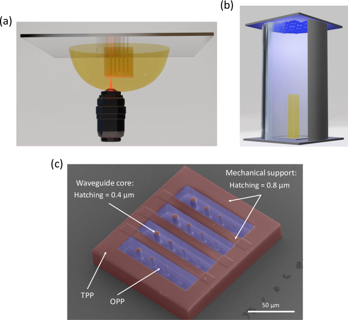
One challenge of 3D TPP following the classical approach is that printing circuits with mm3 volumes quickly results in unfeasible fabrication time in excess of 20h. However, 3D waveguide circuits are defined via the trajectories of waveguide cores, while waveguide claddings are inherently realized through the surrounding, ’unstructured’ volume of a lower refractive index. One can therefore constrain the high-resolution and slow TPP process to creating the waveguide cores, and use indiscriminate, hence fast single-step blanket exposure above the resin photo-initiator’s absorption energy to develop the entire remaining chip in one flash. The working principle of flash-TPP is illustrated in Fig. 1(a-c). Figure 1(a) depicts the usual dip-in TPP printing procedure, where the microscope objective is directly immersed into the resin. The printed structure is then developed using the previously described steps. Next, we transfer the developed circuit to a UV chamber (Rolence Enterprise Inc., LQ-Box model, 405 nm wavelength, 150 mW/cm2 average light intensity) as shown in Fig. 1(b), and we control the OPP dosage via the duration of the UV exposure. Here, we characterize the effects of exposure times between 0 and 60 s.
We further accelerate the fabrication process by locally and dynamically adjusting TPP writing conditions according to the functionality of each circuit’s component. Minimizing propagation losses requires minimizing the roughness at the core-cladding interface and we use a small spacing between voxels in the (x,y)-plane, i.e. with a small hatching distance . At the same time, we can maximize the vertical distance between consecutive slices, or slicing distance , which we found not to significantly affect the core-cladding interface roughness and equally accelerates the printing process. Crucially, the writing power needs to be adjusted in order not to overexpose the TPP-written voxels, which results in micro-explosions and high propagation losses. Other sections, such as the outer cladding of a 3D chip or internal columns for support do not interact with the optical signals, and hence they simply need to be mechanically sturdy. We therefore maximally increase the hatching distance, and since printing time scales this has a significant impact. The structure in Fig. 1(c) shows an scanning electron microscopy (SEM) micrograph that illustrates the overall concept. A circuit is first fabricated in a single 3D direct laser TPP lithography (red region) step, which is followed by OPP via irradiation with the UV light source (blue regions) for several seconds.
III Two-photon polymerization fabrication parameters
We printed a set of five free-standing waveguide cores with m height and m diameter using a range of TPP laser powers (LP) and a constant hatching distance of m on a fused silica substrate. As globally fixed parameters in all our fabrications reported in this article we use a scanning speed of 10 mm/s and a slicing distance of m. A SEM micrograph after development is shown in Fig. 2(a), with LP mW. Waveguide cores shown in the first two images were printed with LP mW and LP mW, which results in rough and inhomogeneous surfaces. Increasing the laser power to 15 mW leads to larger TPP voxels and consequently a smoother surface. In contrast, exceeding LP mW leads to overpolymerized waveguides and burning of the polymer, see the last two images of Fig. 2(a). We therefore select LP mW and proceed to optimize the second parameter by scanning the hatching distance from m, with results shown in the SEM micrographs of Fig. 2(b). The first two micrographs, with respectively m and m, reveal smooth surfaces compared to the last three. We therefore select m for the following investigations because, first, the visual inspection of the surface quality shows only a negligible difference compared to m, but using m reduces the fabrication time by a factor 1.8. Second, for m results were not always reproducible, a finding we attribute to spontaneous micro-burnings within the waveguide’s cores as the smaller hatching distance increases the accumulative TPP-irradiation. SEM analysis showed that for these parameters the diameter of waveguide cores exceed the design-diameter by m due to the non-negligible TPP voxel-size. Hence, for the following investigations we consider the effective diameter .
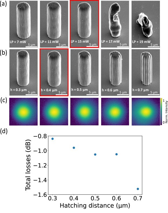
Finally, to carry out an initial evaluation of the propagation losses on the hatching distance , we have characterized five printed waveguides with length of m at nm wavelength with identical parameters as in Fig. 2(b). Figure 2(c) shows the output intensities of the waveguides printed with m at a constant diameter of m with LP mW and m. After development the samples were UV cured during 20s. The first four outputs have practically identical intensity distribution, and a notable reduction in optical confinement can only be found for m. This can also be seen in Fig. 2(d), which characterizes overall optical losses (injection, propagation, outcoupling) on . Overall optical losses slowly grow with until they dramatically increase for m. We consequently select m and LP mW for the fabrication of the TPP-printed waveguide cores, mechanical support structures were printed with low-resolution (m) to reduce printing times. We introduced walls between rows of waveguides in order to maintain a flat top-surface of the cuboids to counteract the effect of shrinkage during sample development, which otherwise results in buckling of the waveguides.
IV Modal confinement
We 3D-printed cuboids embedding 16 waveguides with diameters ranging from m and height of m. We use UV exposure times for the OPP of 0, 5, 20 and 60s, which results in irradiation doses of 0, 750, 3000 and 9000 mJ/cm2, respectively.
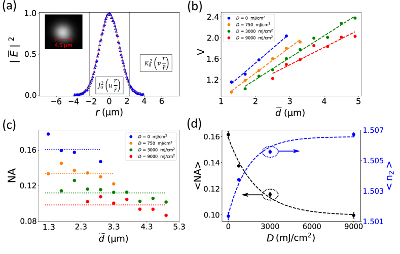
By fitting the experimental output intensities for different diameters, we extract the waveguide’s normalized frequency NA, where NA is the numerical aperture and 1.51 and are the refractive indices of core and cladding, respectively. Each waveguide output intensity is fitted to the fundamental LP01 mode for diameters below the cut-off condition for a second propagating mode, as shown in Fig. 3(a) for an exemplary waveguide of m that was UV cured with = 3000 mJ/cm2. The LP01 mode intensity profile in step-index (STIN) waveguides is described by ( for ¡ and ( for ¿ , where and , the modal parameters Snyder . Therefore, we individually determine the normalized frequency for each waveguide and Fig. 3(b) shows the experimental characterization for all effective waveguides diameters cured using different UV doses . It is clear that the shorter we expose the circuit, the larger the normalized frequency. From the slope of the linear regressions (dashed lines) in Fig. 3(b) we obtain the average NA for each UV exposure, which is shown in Fig. 3(c).
As it can be seen in Fig. 3(c), the NA appears to slightly decrease for larger diameters. We attribute this to the diffusion during development, which leads to a smoother refractive index transition between waveguide core and cladding and consequently converts the STIN profile to an effective gradient index (GRIN) profile Ocier2020 ; TuingZukauskas2015 . This phenomenon would additionally increase the NA for small diameter waveguides.
Finally, Fig. 3(d) shows the evolution of the average numerical aperture ¡NA¿ and refractive index of the cladding on the UV exposure dose. The excellent agreement with the exponential fit demonstrates that we can precisely tune the numerical aperture of the different waveguides, which decreases exponentially till it reaches a plateau. Therefore, considering the refractive index of the core () is approximately constant once fully TPP-polymerized Schmid2019 , all variations of NA versus exposure dose can be assigned to the refractive index of the cladding following , by which we obtain the OPP factor of the IP-S photoresist mJ-1cm2 from the exponential fit.
V Propagation losses
To evaluate losses we fabricated a set of waveguides with lengths spanning from 0.1 to 6 mm. The diameter is m and the UV expose dose = 3000 mJ/cm2, which provide high NA while remaining single-mode. Minimizing injection losses requires adiabatically modifying the waveguide core diameter to transition the mode size of the free-space input to the one of the waveguide. The angle of such tapers, i.e. the taper-rate, needs to be sufficiently small to not excite higher order modes and hence to satisfy the adiabatic transition. We minimized the optical losses of a set of tapers with lengths m and waveguide core diameters m in order to determine the best taper-rate for efficient mode coupling. These we found to be tapering from an taper-input diameter of m to the target waveguide diameter of m during a taper-length of m.
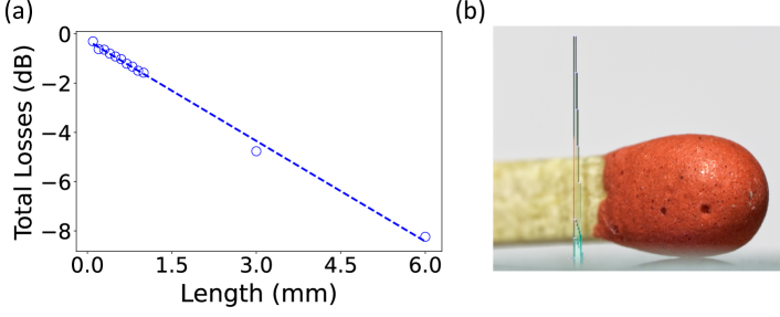
Figure 4(a) depicts the total losses for the fundamental LP01 mode on a semi-logarithmic scale, and via the linear fit we determine -1.36 dB/mm propagation and -0.26 dB injection losses. Our measurements are highly reproducible across the wide range of propagation lengths we here examined, in particular considering that each waveguide longer than 0.5 mm was fabricated on a different substrates. This demonstrates the excellent reproducibility and high quality of our (3+1)D flash-TPP fabrication as well as of our optical characterization.
Propagation losses do not yet reach the bulk absorption of the IP-S photoresist, which is 0.055 dB/mm Schmid2019 , and for now are around one order of magnitude above the current state-of-the-art for standard silicon photonic waveguides Vlasov2004 . Compared to single-pass DLW of waveguides in fused silica glass, our propagation losses are comparable at our characterization wavelength, while we achieve more than an order of magnitude lower injection losses Amorim2019 . Still, our results represent a factor 5 improvement compared to previously 3D-printed waveguides Moughames2021 . Figure 4(b) shows the 6 mm long waveguide printed for this study, imaged next to a match for scale comparison.
VI Temporal stability
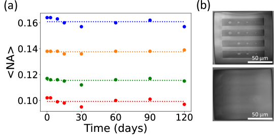
As a final study, we investigated aging of the 3D-printed waveguides, as temporal stability naturally is of vital importance for reliability. Aging could originate from such effects as thermal diffusion Zhang2006 , shrinkage Ovsianikov2009 or undesired photo-polymerization of areas with low degree of polymerization Schmid2019 .
The flash-TPP concept relies on incomplete polymerization of the areas corresponding to waveguide cladding, hence some photo-initiators could remain after development. If unintended post-development optical exposure is sufficient to initiate the photo-initiator’s reactions, the waveguide cladding could in principle be polymerized towards a higher degree, i.e. increasing its refractive index. Consequently, n and the related optical properties would be altered in time. To explore the temporal stability we measured the waveguide’s NA over time. All structures have been kept under standard irradiation intensity of our lab and have not been shielded from room light. As depicted in Fig. 5(a), the NA of all waveguides explored in the previous sections do not suffer any relevant change during their continuous characterization spanning 120 days.
Finally, we also evaluated the waveguide’s resilience to direct sun exposure, for which we placed one sample on a window sill during summer months in central Europe. This resulted in the almost complete polymerization of the cladding area after 15 days and hence the erasure of the light-guiding structures, which can be seen from the microscope image in Fig. 5(b). The direct and unprotected UV radiation from the sun therefore appears to be sufficiently strong Kerr2008 to launch the photo-initiators reaction and thus the polymerization process. We also examined the effect of direct sun exposure on waveguides for which the cladding was printed with a low TPP power dose (i.e. 1, 2 and 3 mW), and no difference compared to the flash-TPP was found; the structures equally got erased by the direct sun exposure. Therefore, we can conclude that the aging under direct exposure to sun light is through the general augmentation in polymerization-degree and does not depend on the polymerization technique used during fabrication.
VII Flash-TPP printing time
Printing time is generally proportional to a circuit’s volume, and the relative time that can be saved due to flash-TPP depends on the ratio between the areas requiring TPP and OPP exposure. Here we assume that this ratio remains constant along a circuit’s z-positions. In previous work on (3+1)D printing we found that waveguides with a radius of m need to be separated by m of cladding in order to have negligible interaction Porte2021 . Cross-talk essentially depends on the relationship of confinement and separation, and scaling of and should therefore remain comparable for integrated single-mode circuits with not too large n. Using TPP to print the entire structure requires a fabrication time , while flash-TPP requires . As a result, the relative duration of flash-TPP relative to classic TPP is given by
| (1) |
which is also the filling factor of waveguide cores within a 3D integrated photonic chip. Therefore, even for a circuit volume with maximal density of waveguide cores, the usual objective of circuit integration, using and defined above the fabrication time is reduced to compared to using TPP alone. This agrees with our experience, where using flash-TPP reduces the printing time to only compared to classical TPP. As a clear example, printing our 6 mm macroscopic structure exclusively using TPP only takes 24 hours, whereas this decreased to 3 hours () using flash-TPP.
VIII Conclusion
We have developed a simple and fast (3+1)D lithography configuration called flash-TPP. This novel manufacturing methodology is based on combining DLW-TPP and OPP, here demonstrated with the commercially available IP-S photoresist, for the fabrication of polymer-cladded single-mode 3D optical waveguides. The flash-TPP concept synergistically combines three princples. First, waveguide cores are printed via DLW-TPP using a precisely calibrated TPP laser power and with high horizontal resolution by minimizing the hatching distances between voxels (m), ensuring low propagation losses due to smooth interfaces. Second, areas purely serving as mechanical support do not interact with the guided wave and no special control of the spacing between TPP-voxels is needed. These are consequently printed with a large hatching distance (m). Finally, instead of building the entire cladding by DLW-TPP, we polymerize in a single instance the integrated photonic circuit via OPP using UV blanket irradiation. Combining these three aspects we are able to reduce the printing time by 90 compared to classical TPP only fabrication. Furthermore, we show that for integrated photonic chips, where the packing density is adjusted to obtain small cross-talk, one can generally expect an acceleration of fabrication on this order.
We demonstrated the high-quality of our (3+1)D flash-TPP fabrication technique. We achieved precise control over the refractive index difference n between waveguide core and cladding by precisely adjusting the UV exposure dose during our blanket OPP illumination, here ranging from 0 to 9000 mJ/cm2. We fitted the waveguide’s output intensities to the LP01 mode of waveguides for variety of UV exposure doses and diameters below the cut-off condition of the second LP mode. From these fits we obtain a robust characterization of a waveguide’s NA as a function of the UV dosage, and our data shows an excellent agreement with the exponential trend expected for saturation processes. This confirmed that we can accurately tune the refractive index of the cladding via adjusting the OPP dosage, obtaining numerical aperture values ranging between NA = 0.10 and NA = 0.16. We finally determined low propagation losses of -1.36 dB/mm and a continuous characterization of our 3D-printed waveguides spanning 120 days demonstrated their temporal stability. In DLW of waveguides in fused silica, post fabrication thermal annealing reduced losses from similar levels down to dB/cm, which could be a promising avenue for approaching the material’s absorption limit.
Overall, we have established the (3+1)D flash-TPP proof of concept as a powerful manufacturing technique towards the fabrication of polymer-based 3D integrated photonic circuits. Our new concept can be particularly advantageous in applications requiring integrated photonics circuits of complex 3D topology that render a standard 2D integration impossible. On this line, our approach presents a very promising concept for future scalable integrations of parallel optical interconnects.
Funding
European Union’s Horizon 2020 (713694); Volkswagen Foundation (NeuroQNet II); Agence Nationale de la Recherche (ANR-17-EURE-0002, ANR-15-IDEX-0003); Region Bourgogne Franche-Comté; French Investissements d’Avenir; French RENATECH network and FEMTO-ST technological facility.
References
- (1) S. Maruo, K. Ikuta, and H. Korogi, “Force-controllable, optically driven micromachines fabricated by single-step two-photon microstereolithography,” Journal of Microelectromechanical Systems, vol. 12, no. 5, pp. 533–539, 2003.
- (2) Q. Ji, J. Moughames, X. Chen, G. Fang, J. J. Huaroto, V. Laude, G. Ulliac, C. Clévy, P. Lutz, K. Rabenorosoa, V. Guelpa, A. Spangenberg, J. Liang, A. Mosset, and M. Kadic, “4d thermomechanical metamaterials for soft microrobotics,” Communications Materials, vol. 2, no. 93, p. 2662, 2021.
- (3) J. D. Pitts, P. J. Campagnola, G. A. Epling, and S. L. Goodman, “Submicron multiphoton free-form fabrication of proteins and polymers: Studies of reaction efficiencies and applications in sustained release,” Macromolecules, vol. 33, no. 5, pp. 1514–1523, 2000.
- (4) H. B. Sun and S. Kawata, Two-Photon Photopolymerization and 3D Lithographic Microfabrication. Springer-Verlag, 2004.
- (5) T. Ergin, N. Stenger, P. Brenner, J. B. Pendry, and M. Wegener, “Three-Dimensional Invisibility Cloak at Optical Wavelengths,” Science, vol. 328, pp. 337–339, 4 2010.
- (6) S. Ristok, S. Thiele, A. Toulouse, A. M. Herkommer, and H. Giessen, “Stitching-free 3d printing of millimeter-sized highly transparent spherical and aspherical optical components,” Optical Materials Express, vol. 10, p. 2370, 10 2020.
- (7) P. Dietrich, M. Blaicher, I. Reuter, M. Billah, T. Hoose, A. Hofmann, C. Caer, R. Dangel, B. Offrein, U. Troppenz, M. Moehrle, W. Freude, and C. Koos, “In situ 3d nanoprinting of free-form coupling elements for hybrid photonic integration,” Nature Photonics, vol. 12, pp. 241–247, 2018.
- (8) N. Lindenmann, G. Balthasar, D. Hillerkuss, R. Schmogrow, M. Jordan, J. Leuthold, W. Freude, and C. Koos, “Photonic wire bonding: a novel concept for chip-scale interconnects,” Optics Express, vol. 20, p. 17667, 2012.
- (9) X. Porte, N. U. Dinc, J. Moughames, G. Panusa, C. Juliano, M. Kadic, C. Moser, D. Brunner, and D. Psaltis, “Direct (3+1)d laser writing of graded-index optical elements,” Optica, vol. 8, p. 1281, 10 2021.
- (10) J. Moughames, X. Porte, M. Thiel, G. Ulliac, L. Larger, M. Jacquot, M. Kadic, and D. Brunner, “Three-dimensional waveguide interconnects for scalable integration of photonic neural networks,” Optica, vol. 7, p. 640, 6 2020.
- (11) J. Moughames, S. Jradi, T. M. Chan, S. Akil, Y. Battie, A. E. Naciri, Z. Herro, S. Guenneau, S. Enoch, L. Joly, J. Cousin, and A. Bruyant, “Wavelength-scale light concentrator made by direct 3D laser writing of polymer metamaterials,” Scientific Reports, vol. 6, p. 33627, 10 2016.
- (12) T. Bückmann, N. Stenger, M. Kadic, J. Kaschke, A. Frölich, T. Kennerknecht, C. Eberl, M. Thiel, and M. Wegener, “Tailored 3d mechanical metamaterials made by dip-in direct-laser-writing optical lithography,” Advanced Materials, vol. 24, no. 20, pp. 2710–2714, 2012.
- (13) W. Lin, D. Chen, S.-C. Chen, and S.-C. Chen, “Emerging micro-additive manufacturing technologies enabled by novel optical methods,” Photonics Research, vol. 8, p. 1827, 12 2020.
- (14) T. Gissibl, S. Thiele, A. Herkommer, and H. Giessen, “Two-photon direct laser writing of ultracompact multi-lens objectives,” Nature Photonics, vol. 10, no. 8, pp. 554–560, 2016.
- (15) N. U. Dinc, J. Lim, E. Kakkava, C. Moser, and D. Psaltis, “Computer generated optical volume elements by additive manufacturing,” Nanophotonics, vol. 9, no. 13, pp. 4173–4181, 2020.
- (16) S. K. Selvaraja and P. Sethi, “Review on optical waveguides,” Emerging Waveguide Technology, 2018.
- (17) J. Moughames, X. Porte, L. Larger, M. Jacquot, M. Kadic, and D. Brunner, “3d printed multimode-splitters for photonic interconnects,” Optical Materials Express, vol. 10, p. 2952, 11 2020.
- (18) A. Nesic, M. Blaicher, T. Hoose, A. Hofmann, M. Lauermann, Y. Kutuvantavida, M. Nöllenburg, S. Randel, W. Freude, and C. Koos, “Photonic-integrated circuits with non-planar topologies realized by 3d-printed waveguide overpasses,” Optics Express, vol. 27, p. 17402, 6 2019.
- (19) J. Pyo, J. T. Kim, J. Lee, J. Yoo, and J. H. Je, “3d printed nanophotonic waveguides,” Advanced Optical Materials, vol. 4, no. 8, pp. 1190–1195, 2016.
- (20) N. U. Dinc, D. Psaltis, and D. Brunner, “Optical neural networks: The 3d connection,” Photoniques, no. 104, pp. 34–38, 2020.
- (21) G. Della Valle, R. Osellame, and P. Laporta, “Micromachining of photonic devices by femtosecond laser pulses,” Journal of Optics A: Pure and Applied Optics, vol. 11, p. 049801, 4 2009.
- (22) A. W. Snyder and J. D. Dove, Optical Waveguide Theory. Chapman and Hall, 1983.
- (23) G. Panusa, Y. Pu, J. Wang, C. Moser, and D. Psaltis, “Fabrication of sub-micron polymer waveguides through two-photon polymerization in polydimethylsiloxane,” Polymers, vol. 12, no. 11, 2020.
- (24) M. Sartison, K. Weber, S. Thiele, L. Bremer, S. Fischbach, T. Herzog, S. Kolatschek, M. Jetter, S. Reitzenstein, A. Herkommer, P. Michler, S. L. Portalupi, and H. Giessen, “3d printed micro-optics for quantum technology: Optimised coupling of single quantum dot emission into a single-mode fibre,” Light: Advanced Manufacturing, vol. 2, no. 1, p. 103, 2021.
- (25) J. Feldmann, K. Weber, S. Thiele, L. Bremer, S. Fischbach, T. Herzog, S. Kolatschek, M. Jetter, S. Reitzenstein, A. Herkommer, P. Michler, S. L. Portalupi, and H. Giessen, “Parallel convolutional processing using an integrated photonic tensor core,” Nature, no. 589, p. 52–58, 2021.
- (26) M. Schmid, D. Ludescher, and H. Giessen, “Optical properties of photoresists for femtosecond 3d printing: refractive index, extinction, luminescence-dose dependence, aging, heat treatment and comparison between 1-photon and 2-photon exposure,” Optical Materials Express, vol. 9, p. 4564, 12 2019.
- (27) H. Sun, K. Takada, M.-S. Kim, K.-S. Lee, and S. Kawata, “Scaling laws of voxels in two-photon photopolymerization nanofabrication,” Applied Physics Letters, vol. 83, pp. 1104–1106, 8 2003.
- (28) T. Gissibl, S. Wagner, J. Sykora, M. Schmid, and H. Giessen, “Refractive index measurements of photo-resists for three-dimensional direct laser writing,” Optical Materials Express, vol. 7, p. 2293, 7 2017.
- (29) Y. Li, S. Park, M. McLamb, M. Lata, S. Schöche, D. Childers, I. D. Aggarwal, M. K. Poutous, G. Boreman, and T. Hofmann, “Uv to nir optical properties of ip-dip, ip-l, and ip-s after two-photon polymerization determined by spectroscopic ellipsometry,” Optical Materials Express, vol. 9, p. 4318, 11 2019.
- (30) J. P. Fouassier and J. Lalevée, Photoinitiators for Polymer Synthesis: Scope, Reactivity, and Efficiency. Wiley, 2012.
- (31) C. R. Ocier, C. A. Richards, D. A. Bacon-Brown, Q. Ding, R. Kumar, T. J. Garcia, J. van de Groep, J.-H. Song, A. J. Cyphersmith, A. Rhode, A. N. Perry, A. J. Littlefield, J. Zhu, D. Xie, H. Gao, J. F. Messinger, M. L. Brongersma, K. C. Toussaint, L. L. Goddard, and P. V. Braun, “Direct laser writing of volumetric gradient index lenses and waveguides,” Light: Science and Applications, vol. 9, p. 196, 12 2020.
- (32) A. Žukauskas, I. Matulaitienė, D. Paipulas, G. Niaura, M. Malinauskas, and R. Gadonas, “Tuning the refractive index in 3d direct laser writing lithography: towards grin microoptics,” Laser and Photonics Reviews, vol. 9, no. 6, pp. 706–712, 2015.
- (33) Y. A. Vlasov and S. J. McNab, “Losses in single-mode silicon-on-insulator strip waveguides and bends,” Optics Express, vol. 12, p. 1622, 4 2004.
- (34) V. A. Amorim, J. M. Maia, D. Viveiros, and P. V. S. Marques, “Loss mechanisms of optical waveguides inscribed in fused silica by femtosecond laser direct writing,” Journal of Lightwave Technology, vol. 37, pp. 2240–2245, 5 2019.
- (35) Z. Zhang, P. Zhao, P. Lin, and F. Sun, “Thermo-optic coefficients of polymers for optical waveguide applications,” Polymer, vol. 47, pp. 4893–4896, 6 2006.
- (36) A. Ovsianikov, X. Shizhou, M. Farsari, M. Vamvakaki, C. Fotakis, and B. N. Chichkov, “Shrinkage of microstructures produced by two-photon polymerization of zr-based hybrid photosensitive materials,” Optics Express, vol. 17, p. 2143, 2 2009.
- (37) J. Kerr and V. Fioletov, “Surface ultraviolet radiation,” Atmosphere-Ocean, vol. 46, no. 1, pp. 159–184, 2008.