Boron phosphide films by reactive sputtering: Searching for a p-type transparent conductor
Abstract
With an indirect band gap in the visible and a direct band gap at a much higher energy, boron phosphide (BP) holds promise as an unconventional p-type transparent conductor. Previous experimental reports deal almost exclusively with epitaxial, nominally undoped BP films by chemical vapor deposition. High hole concentrations were often observed, but it is unclear if native defects alone can be responsible for it. Besides, the feasibility of alternative deposition techniques has not been clarified and optical characterization is generally lacking. In this work, we demonstrate reactive sputtering of amorphous BP films, their partial crystallization in a P-containing annealing atmosphere, and extrinsic doping by C and Si. We obtain the highest hole concentration reported to date for p-type BP () using C doping under B-rich conditions. We also confirm that bipolar doping is possible in BP. An anneal temperature of at least is necessary for crystallization and dopant activation. Hole mobilities are low and indirect optical transitions are much stronger than predicted by theory. Low crystalline quality probably plays a role in both cases. High figures of merit for transparent conductors might be achievable in extrinsically doped BP films with improved crystalline quality.
I Introduction
Numerous III-V semiconductors such as GaAs, InP, GaN and related alloys are technologically mature materials. They are key components of optoelectronic devices such as light emitting diodes, photodetectors, lasers, and high-efficiency solar cells. Boron phosphide (BP) is a relatively under-investigated member of this family in spite of its ultra-high thermal conductivity, Kang et al. (2017) chemical inertness and hardness, Stone and Hill (1960) and prospects for bipolar doping. Shohno et al. (1974) Accordingly, BP has been proposed for several applications such as a corrosion- and heat-resistant coating, Ginley et al. (1983); Kumashiro (1990) photo- and electrocatalyst, Shi et al. (2016); Mou et al. (2019) as well as for thermal management Kang et al. (2017) and extreme UV optics applications. Huber et al. (2016)
More recently, BP was identified as a potential p-type transparent conductive material (TCM). Varley et al. (2017) This is a particularly interesting prospect, because obtaining high p-type conductivity in optically transparent materials is still an unsolved challenge. Fioretti and Morales-Masis (2020); Willis and Scanlon (2021) Unlike the case of other p-type TCM candidates, bipolar doping has been reported in BP by various authors. Shohno et al. (1974); Takigawa et al. (1974); Iwami et al. (1975); Kumashiro (1990); Varley et al. (2017) Thus, BP could be a unique example of a transparent material with both p-type and n-type doping capability.
BP crystallizes in the diamond-derived zincblende structure with tetrahedral coordination. Because the electronegativity difference between B and P is small, BP is a covalent solid and its band structure is closely related to that of Si and C in the diamond structure. The main difference is an intermediate size of the fundamental indirect band gap for BP ( ) Archer et al. (1964); Ha et al. (2020) mainly due to an intermediate bond length. Although this band gap corresponds to visible light, the direct band gap of BP is much wider and falls in the UV region ( ). Schroten et al. (1998); Ha et al. (2020) The weakness of indirect transitions predicted for BP at room temperature Ha et al. (2020) is the key factor that could make BP thin films sufficiently transparent for many TCM applications. For example, a 100 nm-thick BP film is expected to absorb negligible amounts of red-yellow light and less than 10% of violet light according to first-principles calculations including electron-phonon coupling. Ha et al. (2020) With respect to electrical properties, BP has a highly disperse valence band produced by p orbitals, ensuring low hole effective masses (). Varley et al. (2017) Unlike the case of diamond, the valence band maximum of BP lies at a relatively shallow energy with respect to the vacuum level. These are enabling features for high p-type dopability. Zunger (2003); Goyal et al. (2020)
II Open questions in BP research
II.1 Conductivity and transparency
The highest conductivity reported for p-type BP is for a nominally undoped single-crystalline film deposited by chemical vapor deposition (CVD) at using B2H6 and PH3 gas precursors in hydrogen, as reported by Shohno et al.. Shohno et al. (1974) Remarkably, this value is on par with the conductivities of the best n-type TCMs. Gordon (2000) The hole concentration and mobility were and respectively. However, intrinsic defects in BP are not expected to be effective dopants Varley et al. (2017) so the origin of the high carrier concentration is unclear and requires further investigation. In addition, such a high conductivity has not been reproduced by others, with more commonly reported values being in the range for both n-type and p-type BP. Stone and Hill (1960); Wang et al. (1964); Chu et al. (1971); Iwami et al. (1975); Kato et al. (1977); Kumashiro (1990)
A common figure of merit (FOM) for TCMs is the ratio between electrical conductivity and average absorption coefficient in the visible. Gordon (2000); Crovetto et al. (2020) However, the absorption coefficient of BP has rarely been measured. Absorption coefficients of single crystals and single-crystalline films Archer et al. (1964); Wang et al. (1964); Iwami et al. (1975) are generally below at , in line with computational predictions. Yet, a more recent measurement on a BP thin film Odawara et al. (2005) shows a substantially higher absorption coefficient, above in most of the visible region. Furthermore, BP films on transparent substrates are usually described as orange, Chu et al. (1971) red, Takigawa et al. (1974) brown, Iwami et al. (1975) or black, Goossens et al. (1989) indicating that their optical transmission may not be sufficiently high.
The only case where electrical conductivity and absorption coefficient were measured on the same BP sample is the CVD-grown n-type single-crystalline BP film reported by Iwami et al. Iwami et al. (1975) with a FOM of . If we use the absorption coefficient from this study to estimate the FOM of the most conductive p-type BP films reported by Shohno et al., Shohno et al. (1974) we get a FOM of . To contextualize these values, the highest FOM we are aware of for a p-type TCM of any kind is for reactively sputtered CuI. Yang et al. (2016) Thus, BP deserves experimental scrutiny with focus on its applicability as a p-type TCM.
II.2 Film growth
BP is notoriously difficult to synthesize due to the simultaneous presence of a highly inert (B) and a volatile species (P). Woo et al. (2016) High growth temperatures (typically above ) are necessary to activate boron diffusion and obtain crystalline BP, but at these temperatures BP tends to decompose into boron-rich phosphides (such as B6P) and gaseous phosphorus. Kumashiro et al. (1997); Shohno et al. (1974) For this reason, previous thin-film work on BP has given strong preference to CVD processes near atmospheric pressure where it is easier to prevent P losses by keeping a high P partial pressure during deposition. Attempts to grow BP in high vacuum by solid-source evaporation Dalui et al. (2008) and gas-phase molecular beam epitaxy Kumashiro et al. (1997) resulted in amorphous films and insufficient P incorporation at elevated temperatures. Sputter deposition could be a viable alternative because it operates under intermediate pressure conditions. As a non-equilibrium plasma-assisted process, sputter deposition may enable lower temperature growth Yoshioka et al. (2008) and higher dopant solubility in the host material Bikowski et al. (2015) compared to thermal processes. Besides, epitaxial single-crystalline CVD films grown above are of limited applicability in the TCM industry, where cost-effective large-area coating of glass substrates or multilayer stacks are necessary. Magnetron sputtering, on the other hand, is the deposition method of choice for many n-type TCMs in the industry. Morales-Masis et al. (2017); Szyszka (2008); Seo et al. (2020) We are only aware of one previous attempt of sputter deposition of BP. Jia et al. (2011) Optoelectronic characterization was not conducted and it is also unclear if the deposited films actually consisted of BP.
The goal of this work is to answer some of the important open questions elaborated in this section. First, we establish that amorphous BP films can be deposited by reactive sputtering and can be crystallized in a post-annealing step. Second, we find higher absorption coefficients than expected, possibly due to enhanced indirect transitions associated with imperfect crystallinity. Finally, we apply C doping to achieve bipolar conductivity and the highest hole concentration achieved so far in p-type BP. Thus, we confirm that BP can be doped both n-type and p-type, and we propose that BP may reach a high TCM figure of merit by a combination of high crystalline quality and extrinsic doping.
III Results
III.1 One-step growth by reactive sputtering
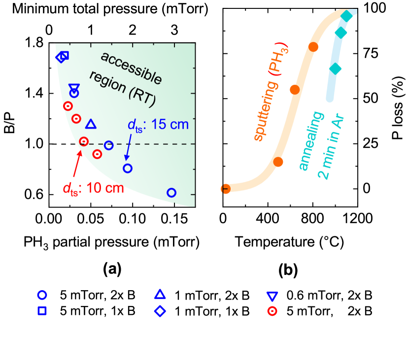
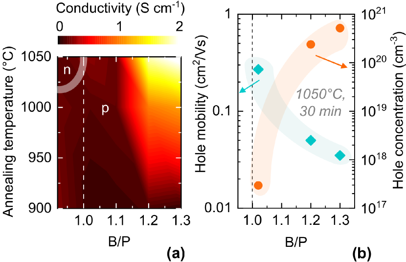
Smooth amorphous BP films can be grown by reactive sputtering of B targets in a PH3/Ar atmosphere. The B/P ratio in the films, as measured by Auger electron spectroscopy (AES), can be continuously adjusted over a wide range at room temperature (Fig. 1(a)). The main factor determining the B/P ratio at fixed temperature is the PH3 partial pressure, with no significant role played by the total sputter pressure and the number of simultaneously sputtering B targets (one or two). A typical oxygen content in the bulk is 2 at.% according to AES.
We infer from these observations that P incorporation in reactively sputtered BP neither occurs as a reaction at the target, nor as a direct reaction of PH3 with elemental B at the substrate. A target reaction would result in an increasing B/P ratio with total pressure at constant PH3 partial pressure, due to a lower fraction of reactive species bombarding the target. A reaction of PH3 with elemental B at the substrate would lead to an increasing B/P ratio with increasing number of co-sputtering B targets. The most likely explanation is that PH3 cracks into more reactive species in the plasma region in front of each target, with subsequent condensation of P at the substrate. The wide continuous range of B/P ratios that can be achieved in the films indicates that P condensation at the substrate results in formation of B-P bonds as well as P-P bonds. Since the flux of reactive P species from PH3 cracking is less directional than the flux of B species ejected from the target, one could expect the films to be more B-rich at larger target-substrate distances, which we indeed observe in our data (Fig. 1(a)). Due to the volatility of P at high temperatures (Fig. 1(b)), a partial pressure of is necessary to obtain at a substrate temperature of . Therefore, sputtering BP at very high temperatures requires either a high PH3 concentration in the sputter gas (beyond the 5% limit dictated by our pre-diluted PH3 bottle) or a high total sputter pressure.
Regardless of substrate temperature ( to ) and stoichiometry (), the conductivity of all as-deposited BP films is too low to be measured on the plane of the substrate with a conventional four-point probe. An upper limit for their conductivity is about , indicating that native defects (such as B and P antisites) are ineffective dopants in this temperature range. To check if these amorphous films could be crystallized, we conducted rapid thermal annealing (RTA) at atmospheric pressure under a continuous Ar flow. Despite the higher total pressure, the lack of a P partial pressure in the system led to rapid P losses. After 2 min at , the films have already lost 65% of their original P content (Fig. 1(b)). Very short anneals at result in broad X-ray diffraction (XRD) peaks attributable to BP. However, the conductivity of all films after RTA is still below . From these initial experiments, we conclude that annealing in a P-containing atmosphere is necessary to prevent P losses and explore a wider process window. It also seems unlikely that intrinsic doping can lead to significant carrier concentrations in BP, so options for extrinsic dopants should be explored.
III.2 Two-step growth by reactive sputtering and annealing with extrinsic doping
To address the issues described above, we post-annealed BP films in sealed quartz ampoules in the presence of sacrificial red phosphorus powder. According to defect calculations, C and Si are the most attractive candidates for p-type doping of BP under B-rich conditions. Varley et al. (2017) We found that C could be easily incorporated into BP by cleaning the ampoules with isopropyl alcohol before annealing (see Experimental Details). The C content of BP films annealed for 30 min is consistently in the 2.5–2.7 at.% range, roughly independent of annealing temperature. This extrinsic dopant concentration is similar to the case of n-type TCMs such as ZnO:Al and In2O3:Sn. Crovetto et al. (2016); Utsumi et al. (2003) AES depth profiles indicate that the C impurities are homogeneously distributed throughout the depth of the films.
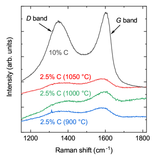
Raman spectra are very sensitive to C impurities in excess of their solubility in the BP matrix, due to the high scattering cross section of the and Raman bands in disordered carbon. Nakamura et al. (1990) Although these Raman bands are already detected at 2.5 at.% C in our samples (Fig. S1, Supporting Information), this C impurity concentration is still sufficiently low not to have a significant effect on the optical properties of BP (Fig. S2, Supporting Information). Based on an empirical relationship between the width of the band and the C crystallite size, Nakamura et al. (1990) we estimate that non-substitutional C segregates in very small clusters around in size. Unless otherwise specified, the post-annealed BP films presented in the rest of the paper are C-doped. The annealing process also results in an increase of the O content in the bulk, from about 2% to about 6%. Two likely reasons are the incomplete removal of air when sealing the ampoules and the traces of isopropyl alcohol responsible for C doping. O impurities are unlikely to act as dopants in BP due to a large size mismatch with P.
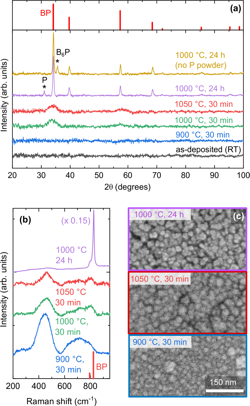
With an annealing time of 30 min, a temperature of is still not sufficient to detect any crystalline BP by XRD (Fig. 2(a)). The corresponding Raman spectrum (Fig. 2(b)) exhibits two broad bands centered at and . These could be attributed to the acoustic and optical phonon bands of zincblende BP with significant broadening. Ha et al. (2020) However, the Raman features of amorphous red phosphorus Fasol et al. (1984) and amorphous B Kuhlmann et al. (1994) are also located in these two spectral regions, so we cannot exclude the presence of the elemental forms of P and B. This film mainly consists of small () particles, with some larger particles that appear brighter in the scanning electron microscope (SEM) and might therefore consist of elemental P (Fig. 2(c)).
When the annealing temperature is increased to , a broad XRD peak with full width at half maximum (FWHM) of appears (Fig. 2(a)). It can be attributed to the (111) reflection in zincblende BP. A similar peak FWHM is obtained after annealing at . Since these widths are much larger than instrumental broadening, and assuming that only size effects are responsible for broadening, we estimate a coherence volume of using the Scherrer equation. This crystallite size is much smaller than the average particle size () determined by SEM (Fig. 2(c)) implying that each particle is poorly crystallized, although some medium-range order exists in some regions. In agreement with these observations, the Raman spectra of the films annealed at and for 30 min resemble the phonon density of states (DOS) calculated for BP. Ha et al. (2020) The peaks at and correspond to the two peaks in the optical phonon DOS. The peak at has a corresponding peak in the acoustic phonon DOS. We will refer to these films as nanocrystalline BP in the rest of the article.
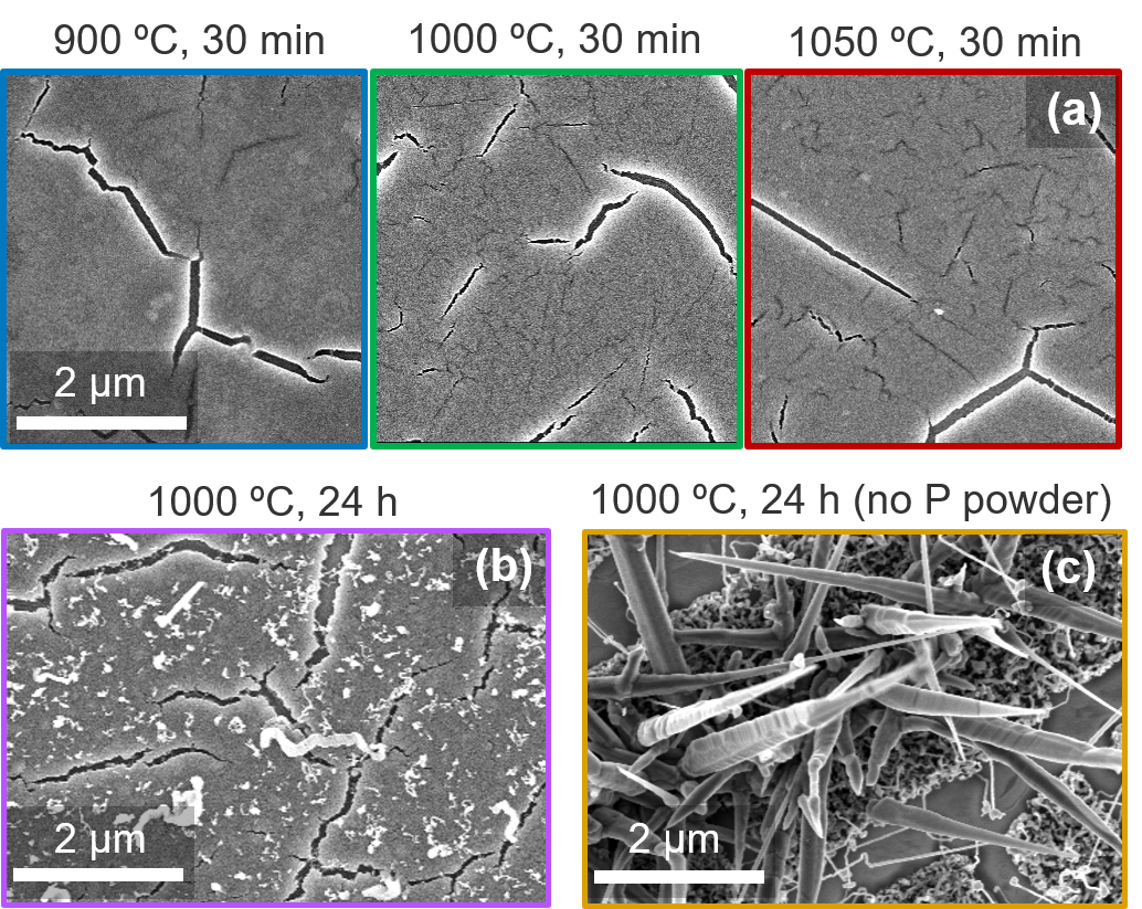
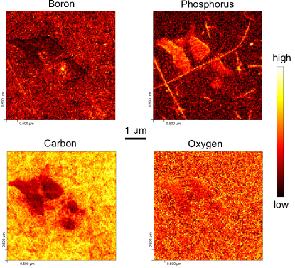
To obtain higher crystalline quality, it is necessary to increase the annealing time. After a 24 h anneal at , all the main XRD peaks of zincblende BP can be detected with a FWHM of for the (111) reflection. Considering the Lorentzian broadening component of this peak and deconvolving instrumental broadening, de Keijser et al. (1982); Crovetto et al. (2016) we estimate a crystallite size of using the Scherrer equation. SEM images of this film (Fig. 2(c)) show that the particle size is still in the diameter range as for the films annealed for a shorter time, but the particle boundaries are much sharper. We conclude that long annealing times enable full crystallization of the (originally amorphous) BP particles, although the particles still do not coalesce into larger grains. The Raman spectrum of this sample (Fig. 2(b)) is similar to spectra reported for high-quality BP crystals and single-crystalline films. Solozhenko et al. (2014); Woo et al. (2016); Padavala et al. (2018) The main peak at and the secondary peak at can be attributed to the Raman-active longitudinal (LO) and transverse (TO) optical phonon modes at the point, respectively. Ha et al. (2020) Our 24 h-long anneals result in phase segregation on the film surface, clearly visible in Fig. 3(b), and in a new XRD peak at (Fig. 2(a)). According to AES imaging (Fig. S3, Supporting Information), these surface secondary phases mainly consist of elemental P. The new XRD peak is compatible with both fibrous red phosphorus Ruck et al. (2005) and Hittorf’s (violet) phosphorus. Hittorf (1865)
If red phosphorus powder is not present during annealing, part of BP decomposes into B6P and gaseous P until the P partial pressure in the ampoule is sufficiently high to prevent further P evaporation. The occurrence of this reaction is confirmed by the XRD peak at , compatible with the highest-intensity reflection of B6P. A peculiar “whisker” morphology develops for some of the remaining BP in these films, with typical whisker diameters of roughly and lengths of a few m (Fig. 3(c). BP whisker growth has sometimes been observed in CVD BP films. Motojima et al. (1980); Schroten et al. (1996); Chu et al. (1971) Finally, we note that all the post-annealed BP films presented here exhibit cracks (Fig. 3), probably due to the thermal expansion coefficient mismatch between BP and the fused silica substrate. Slack and Bartram (1975)
III.3 Optical properties
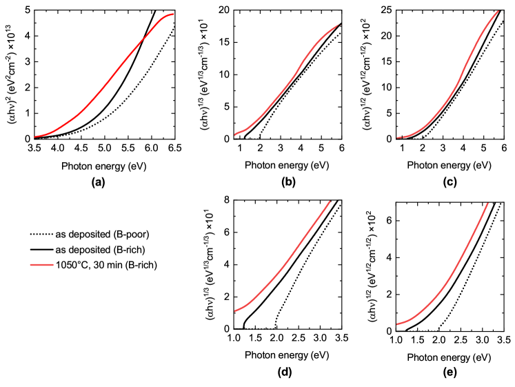
The absorption coefficient of the as-deposited films depends on their stoichiometry, with B-rich films having lower band gaps than B-poor films (Fig. 4(a)). In these amorphous films, versus plots are roughly linear for (Fig. S4, Supporting Information), as usually found in amorphous semiconductors. Davis and Mott (1970) A similar spectral behavior and a decreasing band gap for increasing B content were found for amorphous BxP films by CVD with . Schroten et al. (1999) The band gaps of the B-rich and the B-poor films are estimated as and , respectively (Fig. S4, Supporting Information). Note that the calculated indirect band gap of BP is 1.98 eV using hybrid exchange-correlation functionals. Ha et al. (2020)
The absorption coefficient of the amorphous as-deposited films is much larger than the computational prediction for perfectly crystalline BP below the direct band gap at . This is expected because materials without long-range order do not require phonon participation in optical transitions. To achieve transparent conductivity in amorphous BP, a shift of the fundamental gap to higher photon energies with respect to the crystalline state would be advantageous to widen the transparency window. While this effect is very well known in amorphous Si, Jellison et al. (1993) we do not observe it in amorphous BP. In fact, a very recent molecular dynamics study predicts that amorphous BP should have an even lower band gap than crystalline BP. Bolat and Durandurdu (2021) The reason is that even short-range order is often broken in amorphous BP, with abundant homoelement bonds (B-B and P-P) occurring in B-rich and B-poor clusters. As the band gap of amorphous boron is 1.0 eV, Morita and Yamamoto (1975) the B-rich clusters are likely responsible for band gap narrowing in amorphous BP, as well as its further narrowing under B excess. Schroten et al. (1999) Since this effect is unique to compound semiconductors, it may explain the discrepancy between the optical properties of amorphous BP and amorphous Si, in spite of their similar bonding and electronic structure in the crystalline state.
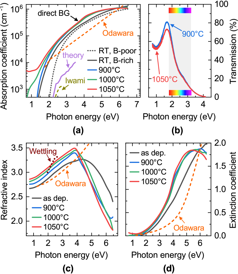
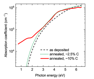
As shown in the next section and as observed by other workers, Shohno et al. (1974); Kumashiro (1990); Varley et al. (2017) B-rich conditions are necessary to achieve appreciable p-type conductivity in BP. Therefore, the remaining optical characterization shown in Fig. 4 focuses on B-rich films with B/P = 1.3. We limit our study to the nanocrystalline films annealed for 30 min, because longer anneals generate very rough films with secondary phases (Fig. 3(b)), so their optical characterization is not reliable. The absorption coefficient of the post-annealed films is overall slightly larger than in the as-deposited film (Fig. 4(a)). The post-annealed films also have a secondary absorption onset in the 4.0-4.5 eV range (Fig. S4, Supporting Information) which is absent from the as-deposited films. This secondary onset is likely associated with the direct band gap of BP, predicted to lie at from computation Ha et al. (2020) and measured at on crystalline BP. Schroten et al. (1998) The primary absorption onset appears to shift to lower photon energies with increasing annealing temperature, although this effect might be an artifact often seen in rough films due to scattering and/or depolarization effects. Swanepoel (1984); Crovetto et al. (2018, 2015) In any case, the visible absorption coefficient of our post-annealed films is over one order of magnitude larger than the absorption coefficient computed for pristine BP Ha et al. (2020) and is also significantly larger than the experimental absorption coefficient determined for an epitaxial CVD film by ellipsometry (Fig. 4(a)). Odawara et al. (2005) As a consequence, the optical transmission of our -thick films drops to very low values in the blue region of the visible (Fig. 4(b)).
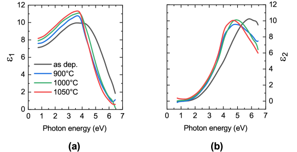
The refractive indices of our films match previous measurements on crystalline films Wettling and Windscheif (1984); Odawara et al. (2005) in the spectral region below the direct gap of BP (Fig. 4(c)). At higher photon energies, the refractive indices decrease due to the inflection point in the extinction coefficient (Fig. 4(d)). The slight increase in the refractive index and extinction coefficient with increasing annealing temperature is probably due to film densification upon annealing. The thickness of the uniform film layer defined in the ellipsometry model plus one half of the roughness layer decreases by 10% between the as-deposited film and the film annealed at (Table S2, Supporting Information). This matches the 10% increase in refractive index seen in Fig. 4(c)). By extrapolating the real part of the complex dielectric function to zero photon energy, we can estimate the high-frequency permittivity of BP, which is in the range for all films (Fig. S5, Supporting Information). These values are consistent with the empirical band gap-permittivity relationship in III-V semiconductors. Sirota (1968) Since BP is strongly covalent, we expect the static permittivity to be nearly equal to .
III.4 Electrical properties
III.4.1 Intrinsic and extrinsic dopants in BP
The origin of the high carrier concentration reported for many BP crystals and films, either p-type Stone and Hill (1960); Wang et al. (1964); Chu et al. (1971); Shohno et al. (1974); Kumashiro (1990) or n-type Shohno et al. (1974); Iwami et al. (1975); Kato et al. (1977); Kumashiro (1990) is unclear. First-principles calculations indicate that the lowest-energy acceptor level in BP is the BP antisite. Varley et al. (2017) However, this defect has a deep charge transition level (more than above the valence band maximum), a high formation energy ( in the p-type regime, even under favorable B-rich conditions), and is highly compensated by the PB donor. A similar situation exists for the dominant PB donor under B-rich conditions. It is therefore unlikely that these native defects can be responsible for the carrier concentrations between and observed in most studies of crystalline BP.
Extrinsic defect calculations Varley et al. (2017) indicate that Si, C, and Be should be more effective substitutional dopants compared to intrinsic defects in BP. All these impurities can dope BP either n-type or p-type depending on whether substitution occurs on the B site (n-type) or on the P site (p-type). Just like the intrinsic defects, B-poor conditions favor n-type conductivity and B-rich conditions favor p-type conductivity. Varley et al. (2017) Takigawa et al. Takigawa et al. (1974) and Kumashiro Kumashiro (1990) had already hypothesized an ”autodoping” mechanism in BP due to diffusion of Si from the substrate into BP. Substantial Si impurity levels ( at growth temperature) were detected in BP by secondary mass ion spectroscopy (SIMS). Kumashiro (1990) The Si content generally increased with increasing growth temperature and was correlated with the carrier concentration in BP. Kumashiro (1990) In general, the highest carrier concentrations reported in previous studies (above ) have been achieved in the cases where BP was deposited on a Si-containing substrate and at high temperatures. Chu et al. (1971); Iwami et al. (1975); Shohno et al. (1974) As another potential source of contamination, we note that the highest purity of elemental boron sources available from commercial suppliers is often only 99.9%. Two different suppliers provided us with boron targets of this overall purity – one with Si, the other with Si. The former target can potentially lead to carrier concentrations up to just due to its Si impurities.
The effect of possible C impurities on the electrical properties of BP has not been discussed in the experimental literature, although C from organic substances and cleaning agents can easily contaminate growth setups. C impurities in solid material sources (including our B sputter targets) are often not documented due to the very low C sensitivity factor of inductively coupled plasma mass spectrometry (ICP-MS), which is typically used for impurity analysis. Houk (1986) However, C is known to be a common impurity in elemental boron. Greenwood and Earnshaw (1997); Yu et al. (2015)
III.4.2 C-doped BP with short post-annealing
The electrical conductivity of BP films annealed for 30 min with 2.5–2.7 at.% C dopant content is shown in Fig. 5(a) as a function of annealing temperature and initial B/P stoichiometry. N-type conductivity is only observed for B-poor films at high annealing temperatures, otherwise the films are p-type. The p-type conductivity increases for increasing B/P ratio, as expected from theory, Varley et al. (2017) and also with increasing annealing temperature (Fig. 5(a)). The maximum p-type conductivity of is achieved for an annealing temperature of and . This conductivity value is in the typically reported range for BP single crystals and crystalline films. Stone and Hill (1960); Wang et al. (1964); Chu et al. (1971); Iwami et al. (1975); Kato et al. (1977); Kumashiro (1990)
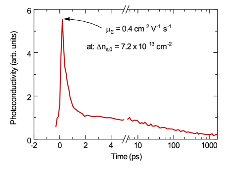
We obtained reliable Hall measurements only on three films annealed at (Fig. 5(b)) using a Hall setup designed for low-mobility samples. These measurements already reveal important differences between our nanocrystalline, C-doped films and previously reported crystalline films. The hole concentration in our B-rich films is well above , significantly higher than in any previous report. As expected, the hole concentration drops by several orders of magnitude when moving from B-rich composition to the nominal stoichiometry (Fig. 5(b)). The hole mobility is near the stoichiometric B/P ratio and it drops by one order of magnitude when moving towards B-rich stoichiometries. An alternative non-contact technique (THz spectroscopy) indicates that the sum of electron and hole mobilities in the nearly stoichiometric BP film is about (Fig. S6, Supporting Information). Due to the very small crystallite size in these films (), we expect THz spectroscopy to be sensitive to the same scattering mechanisms as Hall effect measurements, hence the consistency between the two results. These mobility values are compatible with the only measurement on non-epitaxial, polycrystalline BP that we are aware of (). Goossens et al. (1989) Hole mobilities above have, however, been demonstrated by several authors on single-crystalline BP. Shohno et al. (1974); Wang et al. (1964) The low mobility of our stoichiometric film is likely due to the low crystalline quality obtained with short annealing times. The additional decrease in mobility for B-rich stoichiometries may be due to additional ionized impurity scattering from the CP acceptors and/or to the increased concentration of other crystallographic defects caused by higher nonstoichiometry.
III.4.3 C-doped BP with long post-annealing
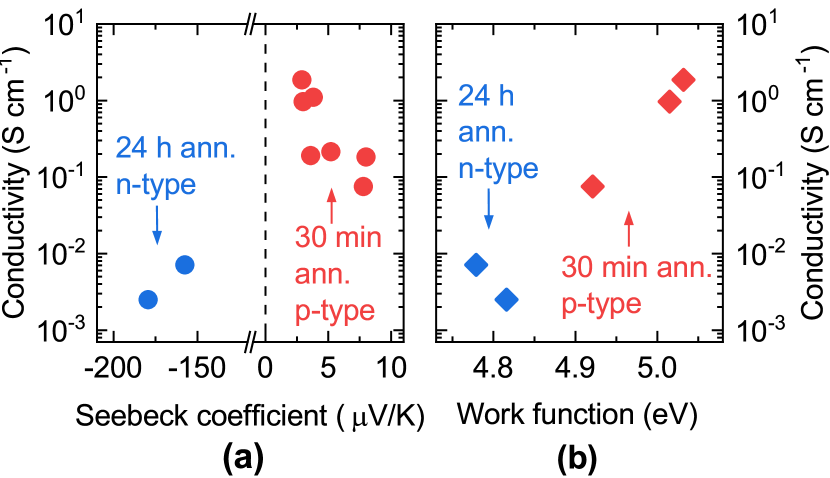
The conductivities of films annealed for 24 h with sacrificial P powder and 2.5% C doping are in the range regardless of initial stoichiometry. Their conductivity might be underestimated due to a high density of cracks (Fig. 3(b)). Nevertheless, Seebeck coefficients in these films are generally much higher in magnitude than the Seebeck coefficients of the films annealed for a shorter time (Fig. 6(a)). Due to the inverse relationship between Seebeck coefficient and carrier concentration, it is then likely that the films annealed for 24 h have much lower carrier concentrations. Another important difference is that films annealed for 24 h have negative Seebeck coefficients, indicating n-type conductivity, unlike the majority of the films annealed for 30 min (Fig. 5(a)). In the following paragraphs we present a hypothesis that could account for the observed differences.
We find that the depth-averaged composition of a BP film after a 30 min anneal at changes from to . Thus, post-annealing in a P-containing atmosphere tends to compensate the original nonstoichiometry and produces nearly stoichiometric BP (). This compensation process is apparently already completed after 30 min. Yet, the measured electrical properties still strongly depend on the B/P ratio of the original as-deposited films (Fig. 5). Hence, the high hole concentrations achieved by annealing B-rich BP for a short time can be considered a non-equilibrium property. In the initial stages of the annealing process, both C and P diffuse into B-rich amorphous BP precursors. Under B-rich conditions, formation of CP acceptor defects is favorable, causing p-type conductivity. For extended annealing times, B-rich conditions no longer exist so the thermodynamically stable concentration of CP acceptors is much lower than the non-equilibrium CP concentration achieved in the initial annealing stages. Thus, a significant decrease in the CP concentration is expected, but this decrease might take a long time to realize because (i) existing B-C bonds have to be broken, and (ii) BP becomes more and more crystalline with time, with a corresponding increase of kinetic barriers. As mentioned above, the final defect concentrations achieved after 24 h under our experimental conditions lead to weak n-type conductivity. The likely reason is that BP slowly becomes slightly P-rich in a P-containing atmosphere. This is compatible with the observation of elemental P secondary phases after long annealing times (Fig. 3(b)).
III.4.4 Work function
According to Kelvin probe measurements, the work function of our BP films only spans a limited range (, Fig. 6(b)), despite the fact that some films annealed for 30 min are degenerately p-type doped and the films annealed for 24 h are n-type. The ionization potential and electron affinity of CVD BP were previously determined as and respectively by electrochemical Mott-Schottky measurements. Goossens et al. (1991) Thus, the surface Fermi level of our BP films is pinned around midgap despite their differences in doping type and concentration. Surface Fermi level pinning is a well-known phenomenon in air-exposed III-V semiconductor surfaces. The Fermi level of n-type and p-type GaAs exposed to oxygen is also pinned within a range around midgap. Spicer et al. (1980) By analogy, we assume that a high density of surface states due to native oxide formation is responsible for the pinning effect in BP.
III.4.5 C versus Si doping in sputtered BP
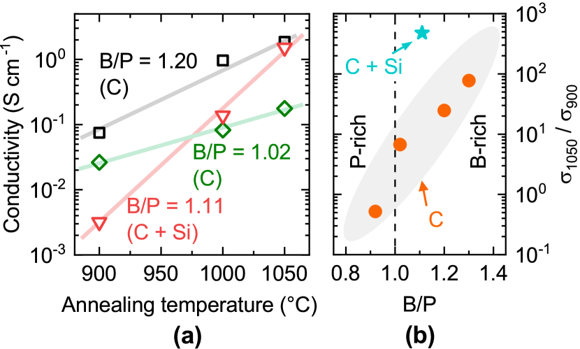
To draw a preliminary comparison between C and Si as potential dopants in BP, we deposited a BP:Si film by reactive cosputtering of a B and a Si target. This film has and a Si content of approximately 2 at.%. Different pieces of this film were annealed for 30 min and co-doped with 2.5 at.% C. We refer to these films as BP:Si,C. P-type conductivity is observed in all the BP:Si,C films after post-annealing. At annealing temperature, the conductivity of BP:Si,C is about the same as the conductivity of a BP:C film with and much higher than the conductivity of a BP:C film with (Fig. 7(a)). The conductivity of all the films (BP:C and BP:Si,C) annealed for 30 min generally has an exponential dependence on annealing temperature (Fig. 7(a)). In Fig. 7(b), we plot the ratio between the conductivity obtained after annealing at and after annealing at, as a function of the B/P ratio. This quantity is a measure of the conductivity increase with increasing annealing temperature. For BP:C films, increases with increasing B/P ratio (Fig. 7(b)). For the BP:Si,C series, is much higher than expected for a BP:C film of the same B/P ratio (Fig. 7(b)).
A possible interpretation of the generally increasing conductivity with annealing temperature is dopant activation, i.e., the thermally-activated incorporation of CP and SiP acceptors in the BP lattice. To explain the higher ratio in BP:Si,C films, one could invoke a higher activation energy for Si diffusion in BP or a higher defect formation energy for the SiP defect. However, these hypotheses do not explain why the BP:Si,C film has a much lower conductivity than all other BP:C films at the lowest annealing temperature (Table S1, Supporting Information). It also does not explain why the ratio for BP:C films increases significantly with increasing B/P ratio. It is important to reiterate that the B/P ratios quoted in this paper are measured before annealing. As discussed above, post-annealing in a P atmosphere tends to restore the stoichiometric B/P ratio of 1. At high annealing temperatures, we expect that B-rich conditions can be maintained for a longer time in films with high initial B/P ratios, explaining their higher ratio.
The observation that the Si-codoped films are the least conductive at low annealing temperature could be rationalized by assuming that SiP defects form more easily than CP defects, but that they are less easily ionized by electrons in the valence band. With this hypothesis, SiP defects would yield a lower concentration of free holes at room temperature compared to an equivalent concentration of CP defects. In fact, this is exactly what was found by first-principles defect calculations. Varley et al. (2017) The CP acceptor has a higher formation enthalpy than SiP at fixed chemical potential ( versus ). However, CP has a much shallower level than SiP ( versus above the valence band maximum).
IV Discussion
It is relatively straightforward to deposit smooth, amorphous BP in a wide range of compositions by reactive sputtering. Nevertheless, this processing route has some disadvantages with respect to CVD. First, B is a very hard element with a much lower sputter yield than the soft metals used in n-type TCMs (e.g., Zn, In, Sn). Since high sputter powers are not viable due to the low thermal conductivity of B, low deposition rates in reactive sputtering of B seem unavoidable. A BP compound target is also expected to have a low sputter yield but it may allow for higher powers due its high thermal conductivity. Kang et al. (2017) A potential advantage of reactively sputtered BP is that the as-deposited amorphous films have a relatively low surface roughness of around RMS for -thick films (Table S2, Supporting Information). BP has been proposed as a material for extreme UV optics but the large roughness of CVD films was found to be a limiting factor. Huber et al. (2016) Thus, reactive sputtering may be a more promising route for this particular application.
Nanocrystalline BP films with small () crystallite size are not sufficiently transparent for TCM applications due to strong absorption above its nominally indirect band gap. High crystalline quality is thus an important requirement for BP and for other candidate TCMs with indirect gaps in the visible. This requirement is much less stringent in direct-gap n-type oxide TCMs, which often have very small grain sizes. Crovetto et al. (2016); Morales-Masis et al. (2017) Unfortunately, reactively sputtered BP films on fused silica are still amorphous even at a substrate temperature of . The crystallinity of BP films can be improved by post-annealing in a P-containing atmosphere but the crystallite size seems to be limited by the particle size of the as-deposited films, without significant coalescence between these particles. The limiting crystallite size obtained by long anneals at high temperatures is in the range. This crystallite size might be sufficient to prevent strong indirect absorption, but we could not draw any conclusion in this regard because our crystalline films have spurious phases at the surface (Fig. 3(b)). Significant light scattering from these phases, as well as their unknown optical properties, makes it difficult to determine the intrinsic absorption coefficient of the underlying BP film.
With short annealing times, very high hole concentrations can be achieved in nanocrystalline BP under B-rich conditions using extrinsic dopants. Higher hole concentrations are realized with C dopants than with Si dopants, probably because CP is significantly shallower than SiP. Since the conductivity of BP films without extrinsic doping was below under all the conditions investigated in this study, we believe that some of the previously reported high carrier concentrations in BP may be due to Si and/or C incorporation from the substrate or other sources.
Long annealing times have the advantage of better BP crystalline quality and the potential for higher optical transmission. However, we encountered three issues. First, a higher density of cracks (Fig. 3(b)). Second, formation of secondary phases which we identified as elemental phosphorus (Fig. S3, Supporting Information). Third, the tendency of B-rich films to reach their stoichiometric B/P ratio by incorporating P from the evaporated P powder (Sec. III.4.3). This tendency limits the achievable hole concentration, because acceptor defects have higher formation energies under stoichiometric conditions. The issue with cracks might be addressed by a different substrate with a higher thermal expansion coefficient. The two other issues could be addressed by optimizing the amount of sacrificial P powder and employing a thermal gradient to avoid condensation of excess P on the BP films. An annealing system with a continuous PH3 flow might be a more practical solution to control P incorporation in the film.
V Conclusion and outlook
Amorphous BP films can be deposited by reactive sputtering in a wide range of compositions. However, they require a post-annealing step at or above in a P-containing atmosphere for crystallization and dopant activation. Our study points to C as a more effective p-type dopant than either Si or native defects in BP. Incorporation of 2.5% C in BP led to the highest hole concentration reported to date for p-type BP (). While an initial B-rich composition generally favors p-type conductivity, it was also possible to obtain n-type conductivity in B-poor films. Thus, we confirm that BP is amenable to bipolar doping, a rare feature in wide band gap materials.
The hole mobilities and optical transmission of our films were too low for TCM applications. The most likely cause is the relatively poor crystalline quality of BP films annealed for a relatively short time. In general, incomplete crystallization will penalize any candidate transparent conductor with an indirect gap in the visible. The reason is that participation of phonons in indirect transitions is not required in the absence of long-range order, so the absorption coefficient will increase with respect to the case of a perfect crystal. It may be possible to improve the optoelectronic properties through longer anneals with optimized process parameters. Nevertheless, single-step deposition processes at higher P partial pressures are more likely to achieve higher crystalline quality and seem to be a more practical solution in general. Based on previously reported mobilities and absorption coefficient in crystalline BP, as well as the high hole concentrations demonstrated in this study, we argue that BP:C has the potential to achieve high TCM figures of merit and certainly deserves further investigation. Depositing C-doped BP by CVD using e.g., a CH4 doping source, might be a promising strategy. In particular, it will be important to clarify if nonepitaxial, polycrystalline BP can achieve similar hole mobilities and optical transparency as single-crystalline films.
High process temperatures seem unavoidable for obtaining high crystalline quality and dopant incorporation in BP, so it is likely that BP TCMs can only find applications as the first layer in a device stack. Still, a TCM on a transparent substrate is the initial layer in many important optoelectronic devices, such as CdTe and perovskite solar cells, Woods-Robinson et al. (2020); Saliba et al. (2018) so device applications are in principle possible. Since post-annealed BP films on fused silica substrates are prone to cracking, alternative refractory and transparent substrates with a higher thermal expansion coefficient might be necessary. BP is itself a refractory material, and this property could be particularly useful as a transparent contact in thin-film optoelectronic technologies requiring high-temperature processing in other functional layers, such as the emerging class of chalcogenide perovskites. Crovetto et al. (2019) As an additional advantage, the thermal conductivity of BP is among the highest known for any material. Kang et al. (2017) In bifacial solar cells lacking a continuous metallic contact and only consisting of materials with low thermal conductivity, BP contacts could have an additional thermal management function. Finally, the possibility of bipolar doping is encouraging for possible applications in transparent electronics.
VI Experimental details
VI.1 Film deposition
Amorphous BP films were deposited on fused silica and crystalline Si substrates by reactive radio-frequency (RF) magnetron sputtering of B targets in an Ar/PH3 atmosphere. We obtained the desired Ar/PH3 ratio by tuning the relative flow rate of a diluted PH3 source (5% in Ar) and a pure Ar source. Due to the very low sputter yield of B, the films were grown under simultaneous sputtering of two 2” B targets from separate magnetron sources. We used a bare 0.25”-thick B target (99.9% purity, Kurt J. Lesker) and a 0.125”-thick B target In-bonded to a Cu backing plate (99.9% purity, Advanced Engineering Materials). The two targets were confocally oriented with respect to the middle of the substrate. The gas inlet inside the deposition chamber was at approximately the same distance from the two targets and from the substrate. The substrates were clamped to a metallic platen, which was heated by infrared lamps. The quoted temperatures are those measured on the metallic platen after the 30 min stabilization time that preceded each deposition. The BP films employed for post-annealing experiments were deposited at room temperature with a total pressure of , a PH3 partial pressure in the range, an RF power of for each target, and a target-substrate distance of . A description of safety measures adopted by the process operators is available elsewhere. Schnepf et al. (2021)
VI.2 Post-annealing
Ampoules for annealing treatments were made from 1220 mm long, 12 mm outer diameter, and 2 mm wall thickness fused silica tubing (Technical Glass Products, OH, USA). The tubes were cut into 400 mm sections using a diamond saw. The open ended 400 mm tube sections were rinsed using water followed by isopropyl alcohol to remove any residual water. Tube sections were then dried using dry compressed air. An oxy-propylene torch was used to pull the 400 mm tube sections into half-ampoules (200 mm sections with a single closed end). As-deposited BP films were cut into mm2 pieces for post-annealing. Two such samples were placed in each half-ampoule. Care was taken to ensure that there was no overlap between the two samples inside of the ampoules. Unless otherwise specified, samples were annealed in a P-containing atmosphere by loading sacrificial red phosphorus powder (3 mg) in the ampoule. Ampoules were then sealed in vacuum after three evacuation (100 mTorr) and purging (Ar) cycles, with a final sealed ampoule length of 120 mm. Under these conditions, the total phosphorus pressure at is estimated as 500 Torr and is expected to consist of gaseous P4 and P2 species in approximately equal concentrations. Bock and Mueller (1984) For the annealing experiments without P powder, the ampoules were sealed under 400 Torr of Ar after the last evacuation step. The ampoules were placed horizontally in a tube furnace (Thermcraft Inc., NC, USA) as close to the control thermocouple as possible. A fixed heating and cooling ramp rate of 20∘C/min was used while the soak time and temperatures were changed as a variable.
VI.3 Characterization
X-ray diffraction measurements were conducted with a Bruker D8 diffractometer using Cu Kα radiation and a 2D detector. To cover the desired range, three frames were collected with the incidence angle fixed at 10∘, 22.5∘, and 35∘ and the detector center fixed at values of 35∘, 60∘, and 85∘ respectively. The diffraction intensity at each angle was integrated over the range measured by the 2D detector. Structural analysis by XRD was complemented by Raman spectroscopy (Renishaw inVia) at excitation and power density.
Film composition was determined by Auger electron spectroscopy (AES, Physical Electronics 710 scanning Auger nanoprobe) with a , primary beam and after removing the native oxide and adsorbed species with an Ar+ beam (). The default sensitivity factors for numerically differentiated B-KLL and P-LMM peaks were used for quantification, which was performed using Physical Electronics MultiPak v9.6.1.7. Unless other-wise specified, the B/P ratios quoted in the article refer to atomic composition of the films before annealing. Scanning electron microscopy (SEM) images were taken with a Hitachi S-3400N instrument with a field emission gun and beam voltage.
Film thickness and optical properties were determined by variable-angle spectroscopic ellipsometry measurements using a J.A. Woollam Co. M-2000 rotating-compensator ellipsometer. Ellipsometry spectra were fitted with a substrate/film/roughness layer model in the CompleteEase software (J.A. Woollam). The fitting parameters were the thicknesses of the film and roughness layers, as well as the dielectric function of the film layer. The latter was represented by a Kramers-Kronig-consistent b-spline function with 0.3 nodes/eV. Optical transmission in the visible and near IR was measured in a home-built setup.
Electrical conductivity was measured on the plane of the substrate by a collinear four-point-probe. Hall carrier concentration and mobility were measured with a Hall measurement station for low-mobility samples (FastHall, LakeShore Cryotronics) in the van der Pauw configuration. The results were validated by reversing the magnetic field and changing the measurement current. In case of inconsistencies, the results were discarded. The ellipsometry-determined film thickness was used in the derivation of the electrical properties.
The Seebeck coefficient was measured in a home-built setup using In contacts and four temperature differences in the vicinity of room temperature. After checking that the thermovoltage depended linearly on the temperature difference, the Seebeck coefficient of BP was determined as the slope of the linear curve minus the Seebeck coefficient of the In contacts. The work function was measured with a SKP SPV LE 450 Kelvin probe (KP Technology) calibrated with a standard Au sample.
Acknowledgements
This project has received funding from the European Union’s Horizon 2020 research and innovation programme under the Marie Skłodowska-Curie grant agreement No 840751 (synthesis, characterization, and analysis work). This work was authored in part at the National Renewable Energy Laboratory, operated by Alliance for Sustainable Energy, LLC, for the U.S. Department of Energy (DOE) under Contract No. DE-AC36-08GO28308. Funding supporting development of synthesis and characterization equipment (A.C.T., R.R.S., A.Z.) was provided by the Office of Science, Office of Basic Energy Sciences. J.M.A. and E.S.T. acknowledge NSF DMR award 1555340. A.C. thanks Joel Basile Varley and Geoffroy Hautier for useful discussions.
References
- Kang et al. (2017) J. S. Kang, H. Wu, and Y. Hu, Nano Letters 17, 7507 (2017).
- Stone and Hill (1960) B. Stone and D. Hill, Physical Review Letters 4, 282 (1960).
- Shohno et al. (1974) K. Shohno, M. Takigawa, and T. Nakada, Journal of Crystal Growth 24-25, 193 (1974).
- Ginley et al. (1983) D. S. Ginley, R. J. Baughman, and M. A. Butler, Journal of The Electrochemical Society 130, 1999 (1983).
- Kumashiro (1990) Y. Kumashiro, Journal of Materials Research 5, 2933 (1990).
- Shi et al. (2016) L. Shi, P. Li, W. Zhou, T. Wang, K. Chang, H. Zhang, T. Kako, G. Liu, and J. Ye, Nano Energy 28, 158 (2016).
- Mou et al. (2019) S. Mou, T. Wu, J. Xie, Y. Zhang, L. Ji, H. Huang, T. Wang, Y. Luo, X. Xiong, B. Tang, and X. Sun, Advanced Materials 31, 1903499 (2019).
- Huber et al. (2016) S. P. Huber, V. V. Medvedev, J. Meyer-Ilse, E. Gullikson, B. Padavala, J. H. Edgar, J. M. Sturm, R. W. E. van de Kruijs, D. Prendergast, and F. Bijkerk, Optical Materials Express 6, 3946 (2016).
- Varley et al. (2017) J. B. Varley, A. Miglio, V.-A. Ha, M. J. van Setten, G.-M. Rignanese, and G. Hautier, Chemistry of Materials 29, 2568 (2017).
- Fioretti and Morales-Masis (2020) A. N. Fioretti and M. Morales-Masis, Journal of Photonics for Energy 10, 042002 (2020).
- Willis and Scanlon (2021) J. Willis and D. O. Scanlon, Journal of Materials Chemistry C (2021), 10.1039/D1TC02547C.
- Takigawa et al. (1974) M. Takigawa, M. Hirayama, and K. Shohno, Japanese Journal of Applied Physics 13, 411 (1974).
- Iwami et al. (1975) M. Iwami, T. Tohda, and K. Kawabe, Electrical Engineering in Japan 95, 19 (1975).
- Archer et al. (1964) R. J. Archer, R. Y. Koyama, E. E. Loebner, and R. C. Lucas, Physical Review Letters 12, 538 (1964).
- Ha et al. (2020) V.-A. Ha, B. Karasulu, R. Maezono, G. Brunin, J. B. Varley, G.-M. Rignanese, B. Monserrat, and G. Hautier, Physical Review Materials 4, 065401 (2020), arXiv:2004.05390 .
- Schroten et al. (1998) E. Schroten, A. Goossens, and J. Schoonman, Journal of Applied Physics 83, 1660 (1998).
- Zunger (2003) A. Zunger, Applied Physics Letters 83, 57 (2003).
- Goyal et al. (2020) A. Goyal, P. Gorai, S. Anand, E. S. Toberer, G. J. Snyder, and V. Stevanović, Chemistry of Materials 32, 4467 (2020).
- Gordon (2000) R. G. Gordon, MRS Bulletin 25, 52 (2000).
- Wang et al. (1964) C. C. Wang, M. Cardona, and A. G. Fischer, RCA Review 25 (1964).
- Chu et al. (1971) T. L. Chu, J. M. Jackson, A. E. Hyslop, and S. C. Chu, Journal of Applied Physics 42, 420 (1971).
- Kato et al. (1977) N. Kato, W. Kammura, M. Iwami, and K. Kawabe, Japanese Journal of Applied Physics 16, 1623 (1977).
- Crovetto et al. (2020) A. Crovetto, H. Hempel, M. Rusu, L. Choubrac, D. Kojda, K. Habicht, and T. Unold, ACS Applied Materials and Interfaces 12, 48741 (2020).
- Odawara et al. (2005) M. Odawara, T. Udagawa, and G. Shimaoka, Japanese Journal of Applied Physics 44, 681 (2005).
- Goossens et al. (1989) A. Goossens, E. M. Kelder, and J. Schoonman, Berichte der Bunsengesellschaft für physikalische Chemie 93, 1109 (1989).
- Yang et al. (2016) C. Yang, M. Knei, M. Lorenz, and M. Grundmann, Proceedings of the National Academy of Sciences 113, 12929 (2016).
- Woo et al. (2016) K. Woo, K. Lee, and K. Kovnir, Materials Research Express 3, 074003 (2016).
- Kumashiro et al. (1997) Y. Kumashiro, T. Yokoyama, T. Sakamoto, and T. Fujita, Journal of Solid State Chemistry 133, 269 (1997).
- Dalui et al. (2008) S. Dalui, S. Hussain, S. Varma, D. Paramanik, and A. Pal, Thin Solid Films 516, 4958 (2008).
- Yoshioka et al. (2008) S. Yoshioka, F. Oba, R. Huang, I. Tanaka, T. Mizoguchi, and T. Yamamoto, Journal of Applied Physics 103, 014309 (2008).
- Bikowski et al. (2015) A. Bikowski, M. Rengachari, M. Nie, N. Wanderka, P. Stender, G. Schmitz, and K. Ellmer, APL Materials 3, 060701 (2015).
- Morales-Masis et al. (2017) M. Morales-Masis, S. De Wolf, R. Woods-Robinson, J. W. Ager, and C. Ballif, Advanced Electronic Materials 3, 1600529 (2017).
- Szyszka (2008) B. Szyszka, in Transparent Conductive Zinc Oxide: Basics and Applications in Thin Film Solar Cells, edited by K. Ellmer, A. Klein, and B. Rech (Springer, Berlin, 2008) p. 221.
- Seo et al. (2020) H.-S. Seo, W. Cao, J. C. Xiao, Y.-C. Wu, B. Zhao, X. ZHANG, and X. Yan, SID Symposium Digest of Technical Papers 51, 301 (2020).
- Jia et al. (2011) Z. Jia, J. Zhu, C. Jiang, W. Shen, J. Han, and R. Chen, Applied Surface Science 258, 356 (2011).
- Xia et al. (1993) H. Xia, Q. Xia, and A. L. Ruoff, Journal of Applied Physics 74, 1660 (1993).
- Morosin et al. (1986) B. Morosin, A. W. Mullendore, D. Emin, and G. A. Slack, in AIP Conference Proceedings, Vol. 140 (AIP, 1986) pp. 70–86.
- Solozhenko et al. (2014) V. L. Solozhenko, O. O. Kurakevych, Y. Le Godec, A. V. Kurnosov, and A. R. Oganov, Journal of Applied Physics 116, 033501 (2014).
- Crovetto et al. (2016) A. Crovetto, T. S. Ottsen, E. Stamate, D. Kjær, J. Schou, and O. Hansen, Journal of Physics D: Applied Physics 49, 295101 (2016).
- Utsumi et al. (2003) K. Utsumi, H. Iigusa, R. Tokumaru, P. Song, and Y. Shigesato, Thin Solid Films 445, 229 (2003).
- Nakamura et al. (1990) K. Nakamura, M. Fujitsuka, and M. Kitajima, Physical Review B 41, 12260 (1990).
- Fasol et al. (1984) G. Fasol, M. Cardona, W. Hönle, and H. von Schnering, Solid State Communications 52, 307 (1984).
- Kuhlmann et al. (1994) U. Kuhlmann, H. Werheit, T. Lundström, and W. Robers, Journal of Physics and Chemistry of Solids 55, 579 (1994).
- de Keijser et al. (1982) T. H. de Keijser, J. I. Langford, E. J. Mittemeijer, and A. B. P. Vogels, Journal of Applied Crystallography 15, 308 (1982).
- Padavala et al. (2018) B. Padavala, H. Al Atabi, L. Tengdelius, J. Lu, H. Högberg, and J. Edgar, Journal of Crystal Growth 483, 115 (2018).
- Ruck et al. (2005) M. Ruck, D. Hoppe, B. Wahl, P. Simon, Y. Wang, and G. Seifert, Angewandte Chemie International Edition 44, 7616 (2005).
- Hittorf (1865) W. Hittorf, Annalen der Physik und Chemie 202, 193 (1865).
- Motojima et al. (1980) S. Motojima, S. Yokoe, and K. Sugiyama, Journal of Crystal Growth 49, 1 (1980).
- Schroten et al. (1996) E. Schroten, A. Goossens, and J. Schoonman, Journal of Applied Physics 79, 4465 (1996).
- Slack and Bartram (1975) G. A. Slack and S. F. Bartram, Journal of Applied Physics 46, 89 (1975).
- Davis and Mott (1970) E. A. Davis and N. F. Mott, Philosophical Magazine 22, 0903 (1970).
- Schroten et al. (1999) E. Schroten, A. Goossens, and J. Schoonman, Journal of The Electrochemical Society 146, 2045 (1999).
- Jellison et al. (1993) G. E. Jellison, M. F. Chisholm, and S. M. Gorbatkin, Applied Physics Letters 62, 3348 (1993).
- Bolat and Durandurdu (2021) S. Bolat and M. Durandurdu, Journal of Non-Crystalline Solids 570, 121006 (2021).
- Morita and Yamamoto (1975) N. Morita and A. Yamamoto, Japanese Journal of Applied Physics 14, 825 (1975).
- Wettling and Windscheif (1984) W. Wettling and J. Windscheif, Solid State Communications 50, 33 (1984).
- Swanepoel (1984) R. Swanepoel, Journal of Physics E: Scientific Instruments 17, 896 (1984).
- Crovetto et al. (2018) A. Crovetto, A. Cazzaniga, R. B. Ettlinger, J. Schou, and O. Hansen, Solar Energy Materials and Solar Cells 187, 233 (2018).
- Crovetto et al. (2015) A. Crovetto, A. Cazzaniga, R. B. Ettlinger, J. Schou, and O. Hansen, Thin Solid Films 582, 203 (2015).
- Sirota (1968) N. N. Sirota, in Semiconductors and Semimetals, Voume 4 (Elsevier, 1968) p. 156.
- Houk (1986) R. S. Houk, Analytical Chemistry 58, 97A (1986).
- Greenwood and Earnshaw (1997) N. N. Greenwood and A. Earnshaw, Chemistry of the Elements, 2nd ed. (Butterworth-Heineman, Oxford, 1997) pp. 140–143.
- Yu et al. (2015) D. Yu, C. Kong, J. Zhuo, S. Li, and Q. Yao, Science China Technological Sciences 58, 2016 (2015).
- Goossens et al. (1991) A. Goossens, E. M. Kelder, R. J. M. Beeren, C. J. G. Bartels, and J. Schoonman, Berichte der Bunsengesellschaft für physikalische Chemie 95, 503 (1991).
- Spicer et al. (1980) W. E. Spicer, I. Lindau, P. Skeath, C. Y. Su, and P. Chye, Physical Review Letters 44, 420 (1980).
- Woods-Robinson et al. (2020) R. Woods-Robinson, T. Ablekim, A. Norman, S. Johnston, K. A. Persson, M. O. Reese, W. K. Metzger, and A. Zakutayev, ACS Applied Energy Materials 3, 5427 (2020).
- Saliba et al. (2018) M. Saliba, J.-P. Correa-Baena, C. M. Wolff, M. Stolterfoht, N. Phung, S. Albrecht, D. Neher, and A. Abate, Chemistry of Materials 30, 4193 (2018).
- Crovetto et al. (2019) A. Crovetto, R. Nielsen, M. Pandey, L. Watts, J. G. Labram, M. Geisler, N. Stenger, K. W. Jacobsen, O. Hansen, B. Seger, I. Chorkendorff, and P. C. K. Vesborg, Chemistry of Materials 31, 3359 (2019).
- Schnepf et al. (2021) R. R. Schnepf, A. Crovetto, P. Gorai, A. Park, M. Holtz, K. Heinselman, S. R. Bauers, M. M. Tellekamp, A. Zakutayev, A. L. Greenaway, E. Toberer, and A. C. Tamboli, Journal of Materials Chemistry C , DOI:10.1039/D1TC04695K (2021).
- Bock and Mueller (1984) H. Bock and H. Mueller, Inorganic Chemistry 23, 4365 (1984).
SUPPORTING INFORMATION
Conductivity (S/cm)
| B/P = 0.92 (C-doped) | |||
|---|---|---|---|
| B/P = 1.02 (C-doped) | |||
| B/P = 1.20 (C-doped) | |||
| B/P = 1.30 (C-doped) | |||
| B/P = 1.11 (C,Si-doped) |
| BP thickness (nm) | Roughness layer thickness (nm) | RMS roughness (nm) | |
| as-deposited | 134 | 3.4 | 2.0 |
| 123 | 20 | 13 | |
| 121 | 16 | 10 | |
| 116 | 18 | 12 |
Supplementary references
References
- Nakamura, Fujitsuka, and Kitajima (1990) K. Nakamura, M. Fujitsuka, and M. Kitajima, Physical Review B 41, 12260 (1990).
- Davis and Mott (1970) E. A. Davis and N. F. Mott, Philosophical Magazine 22, 0903 (1970).
- Schroten, Goossens, and Schoonman (1999) E. Schroten, A. Goossens, and J. Schoonman, Journal of The Electrochemical Society 146, 2045 (1999).
- Koh et al. (1996) J. Koh, Y. Lu, C. R. Wronski, Y. Kuang, R. W. Collins, T. T. Tsong, and Y. E. Strausser, Applied Physics Letters 69, 1297 (1996).
- Hempel et al. (2018) H. Hempel, C. J. Hages, R. Eichberger, I. Repins, and T. Unold, Scientific Reports 8, 14476 (2018).