Cascode Cross-Coupled Stage High-Speed Dynamic Comparator in 65 nm CMOS
Abstract
Dynamic comparators are the core of high-speed, high-resolution analog-to-digital converters (ADCs) used for communication applications. Most of the dynamic comparators attain high-speed operation only for sufficiently high input difference voltages. The comparators’ performance degrades at small input difference voltages due to a limited pre-amplifier gain, which is undesirable for high-speed, high-resolution ADCs. To overcome this drawback, a cascode cross-coupled dynamic comparator is proposed. The comparator improves the differential gain of the pre-amplifier and reduces the common-mode voltage seen by the latch, which leads to a much faster regeneration at small input difference voltages. The proposed comparator is designed, simulated, and compared with the state-of-the-art techniques in a 65 nm CMOS technology. The results show that the proposed comparator achieves a delay of 46.5 ps at 1 mV input difference, and a supply of 1.1 V.
Index Terms:
Dynamic comparator, high-speed analog-to-digital converters, cascode cross-coupled pair.I Introduction
Analog-to-digital converters are widely used in various applications due to the increased demand for mixed-signal systems [1]. Comparator, an essential block in ADCs, plays a vital role in determining the speed and accuracy of the ADCs. The performance of an ADC relies on the robustness of the comparator [2], especially for low noise, low-power, and high-speed operations. Dynamic comparators are preferred in low-power and high-speed designs due to their zero static power. They are classified as single-tail (ST) and double-tail (DT) topologies. Various ST circuits are reported to suffer from trade-offs between energy consumption (EC), offset, and speed [3]. ST topology also suffers from large kickback (KB) noise and requires a large voltage headroom since the input transistors are directly stacked with the cross-coupled pair. Due to these drawbacks, the DT configuration is preferred for the design of high-speed comparators [4].
Designing a high-speed comparator that can resolve small input difference voltages while holding on to the high-speed capability over a wide range of common-mode voltage is challenging [5]. The conventional DT comparator reported in [6] has mitigated the drawbacks of the ST comparator. However, it fails to give valid outputs for small input difference voltages. This has a direct impact on the resolution of ADCs. Moreover, at higher common-mode levels, the performance of the conventional DT comparator degrades because the input pair enters the triode region without providing sufficient gain. A dynamic comparator resistant to common-mode variations with delayed operation of the latch is presented in [7]. However, it requires a large area and suffers from increased KB noise. Further, the insufficient pre-amplifier gain makes it impractical to use in high precision ADCs. In the dynamic bias DT comparator presented in [8] the pre-amplifier partially discharges the drains of the input transistor pair to reduce EC. However, the speed is compromised to attain energy efficiency. To improve the latch regeneration time, a transconductance-enhanced latch stage is presented in [9]. It has the same drawback as the conventional DT comparator in its common-mode performance. Additionally, due to stacking in the latch stage, the delay increases swiftly for lower supply voltages.
Our work targets to reduce the comparator delay by enhancing the pre-amplifier gain compared to other high-speed DT architectures reported. The performance improvement is achieved by including a cascode cross-coupled pair in the pre-amplifier stage. The circuit is designed and implemented in a 65 nm CMOS technology with a 1.1 V supply. The proposed technique offers better delay performance throughout the input voltage range, especially at smaller input differences. Also, the cascode cross-coupled pair alleviate the delay degradation at higher common-mode voltages. These advantages make the proposed comparator suitable for high-speed, high resolution ADCs.
II Conventional Double Tail Dynamic Comparator
The conventional DT dynamic comparator has an input stage and a latch stage that have separate tail transistors. Two independent tail currents enable us to optimize the design trading-off speed, offset, and EC. This topology has fewer transistors stacked [10], making it suitable for low voltage applications. It also reduces the KB noise due to the isolation between the input transistors and the output nodes.
In the conventional DT, at smaller input difference voltages (), the latch is unable to sense the differential voltage due to the limited differential gain of the pre-amplifier. The proposed comparator mitigates this drawback by lowering the common-mode voltage and improving the differential voltage at the pre-amplifier output. This helps the latch to regenerate faster even at smaller .
III Proposed Cascode Cross-Coupled Dynamic Comparator
A PMOS cross-coupled pair is employed to increase the differential gain of the pre-amplifier in [11]. To enhance the performance further, the proposed topology, shown in Fig. 1, introduces a cascode cross-coupled pair made up of , , , and . As a result, a higher difference voltage, , at the pre-amplifier output nodes (, ) is observed by the latch. This helps to reduce latch regeneration time and to resolve for smaller .

III-A Operation
During the reset phase (), the tail transistors and are off along with the cascode transistors and . The switching transistors and charge the and nodes to . Similarly, and charge the drain nodes of and to . Therefore, and are off. The transistors and ensure a proper start condition for the comparator. During the comparison phase (), and are on, and are off. In the beginning of this phase, the PMOS cascode cross-coupled pair is still inactive, and the transistors and are on. In this scenario, the operation of the pre-amplifier in the proposed circuit resembles that of its conventional counterpart.
When , the node discharges faster and provides sufficient source to gate voltage for to turn on. When turns on first, node starts charging to through . Simultaneously, of falls below the threshold voltage, restricting the current through and to the node . Hence, the node charges to and the node discharges to 0 V. The PMOS cascode cross-coupled structure increases the differential voltage . Subsequently, the initial voltage difference sensed by the latch before regeneration, , is improved as demonstrated below. NMOS transistor switches and take care of the static power dissipation in the pre-amplifier. They also contribute to the increased by manifesting another NMOS cascode cross-coupled pair with the input transistors and . As a result, the latch regeneration time is decreased.
To demonstrate the enhanced , the procedure used in [5] is adopted. The delay analysis of the conventional DT comparator holds for the proposed comparator for most parts except for calculating the gain from input to the and nodes.
III-B Delay Analysis
The delay of the proposed comparator is the sum of amplification time, , and the latch delay time, . The latch delay is given by [5]
| (1) | ||||
where , is the common-mode voltage seen by the latch, and . This equation indicates that a higher , implying a higher , and a lower provide a smaller delay. The proposed comparator achieves both with the help of the cascode cross-coupled pair.
To demonstrate the efficacy of the proposed comparator, the half circuit analysis can be used. Here, transistors and are modelled as current sources as they operate in the saturation region in the initial stages of the comparison phase. Transistors and are in the saturation region as their gate terminals are at ground potential.
Applying KCL at nodes and gives the following expressions
| (2) |
where is the parasitic capacitance at nodes and , , and are the drain currents of and , respectively. is the current gain provided by the common gate stage formed by the cascode transistors and , which is less than unity. Using the small signal analysis can be expressed as
| (3) |
where and are the channel resistance and transconductance of cascode transistors, respectively, and is the source resistance.
By solving the linear equations (2), we get
| (4) |
The common-mode voltage at the pre-amplifier output is given by . By substituting (4) in , we get
| (5) |
where .
The differential voltage at the pre-amplifier output nodes is expressed as and is given by
| (6) |
where .
From (5) and (6), the factor obtained due to the cascode cross-coupled pair reduces the common-mode voltage and improves the differential voltage at and nodes. This helps the latch to regenerate faster than the other comparator architectures. Reducing the of and will also achieve the same result but at the cost of an increased offset voltage.
IV Results and Discussion
 |
| (a) |
| (b) |
The performance metrics of analog circuits, in general, are technology-dependent. Dynamic comparators are no exception and are prone to both analog and digital non-idealities. Therefore, to make a fair comparison between the proposed and the reported dynamic comparator topologies, all the comparators are simulated in 65 nm technology with a minimum channel length of 60 nm, load capacitance of 2 fF, of , of 1.1 V, and of 0.77 V. It is also ensured that all the comparators are designed and optimized to obtain a similar offset standard deviation, .
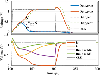
Schematic level transient analysis results of the comparator is shown in Fig. 2. The reference input, , is fixed at 0.77 V to attain the optimum performance [11]. The voltages at the output nodes, and and the intermediate nodes are shown at a of 10 mV. The delay is evaluated when the output node voltages attain a difference of . The delay of the proposed comparator is found to be 33.3 ps whereas, it is 39.3 ps for the conventional one.
Fig. 3 presents the delay variation with at a of 0.77 V. The delay of the proposed comparator is significantly lower over the input difference voltage range. Especially, for lower values, where the comparator presented in [11] and the conventional comparator fail to give valid outputs. It can be seen in the inset of Fig. 3. This can be attributed to the cascode cross-coupled pre-amplifier, which provides sufficient for the latch to regenerate even at lower input difference voltages. From simulation results, it is observed that the proposed comparator is 25 % faster than the conventional comparator and 15 % faster than the [11] at a of 1 mV. This advantage allows us to incorporate this topology in high-speed, high-resolution ADCs provided proper care is taken in the design to reduce the input-referred noise.
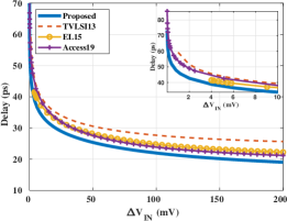
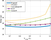
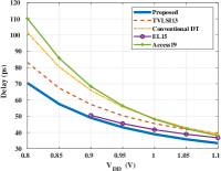
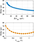
Fig. 4(a) depicts the simulated delay variation with the . For a sufficiently large , the proposed comparator is faster than the state-of-the-art comparators. Conventional DT architectures enter the triode region and thus limits pre-amplifier gain. The proposed topology overcomes this problem to some extent by achieving higher with the help of the cascode cross-coupled pair. Fig. 4(b) shows the simulation results of the delay versus the supply voltage. As expected, the delay performance worsens at lower . However, the plot shows that at lower , the speed of the proposed circuit is 30 % faster than the conventional one.
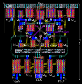
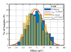
To confirm the high-speed characteristic of the proposed comparator, a layout is drawn as shown in Fig. 5 with proper care to attain symmetry with equal capacitance at the differential nodes to steer off the aspects that increase the delay of the comparator. Monte-Carlo simulations of 200 runs were performed to observe the standard deviation of the offset voltage, . The results are shown in Fig. 6(a). of 11.38 mV is observed from the pre-layout simulations and 11.52 mV is obtained from the post-layout simulations. The offset deviation is slightly more than [11] due to the mismatch contribution of and .The post-layout simulation results of the delay variation with input voltage and the common-mode voltage are shown in Fig. 6(b). An increase in delay due to the layout parasitic capacitance is evident from the post-layout results.
Various performance metrics of the proposed topology along with that of the state-of-the-art topologies are obtained for similar values and the comparison is shown in Table I. The power-delay product (PDP) is obtained at a of 1 mV and tabulated in Table I. PDP can be used as a figure of merit to compare the performance of the topologies. The proposed comparator has better PDP for the speed it offers. In latched comparators, the large voltage variations on the regeneration nodes cause kickback noise. It has been reported that faster comparators generate more kickback noise [12]. This trend can be seen in the proposed comparator as well. However, differential-mode KB causes no harm as long as the comparator is reset before every decision. KB also has a trade-off with offset, RMS noise, and pre-amplifier gain. Additionally, input-referred RMS noise is calculated from the transient noise simulations as explained in [13]. Input is applied and incremented in steps of 10 uV to obtain the probability of error as 16% to get the total input-referred RMS noise and is tabulated.
| Offset | KB | EC/ | RMS | Delay () | PDP | ||
| noise | bit | noise | |||||
| V | () | () | () | (mV) | 10 | 1 | 1 mV |
| V | (pJ.ps) | ||||||
| JSSC ’04[14] | 9.9 | 2.8 | 27.4 | 1.3 | 46.8 | – | |
| ISSCC ’07[6] | 10.2 | 3 | 48.1 | 1.5 | 39.3 | – | |
| JSSC ’10[15] | 9.5 | 7.9 | 82.9 | 0.16 | 52.6 | 67.9 | 6.9 |
| TVLSI ’13[11] | 10.9 | 3.0 | 59.3 | 0.6 | 38.3 | 59.3 | 4.2 |
| EL’15 [7] | 13.6 | 3.3 | 44.9 | 2.6 | 36.7 | – | |
| TVLSI ’18[5] | 15.1 | 51.8 | 41.7 | 3.5 | 56.7 | – | |
| JSSC ’18[8]∗ | 8.9 | 2.4 | 32.9 | 0.5 | 119.8 | – | |
| Access ’19[9] | 11.5 | 3.7 | 83.3 | 0.5 | 38.1 | 53.9 | 4.98 |
| TCASII ’20[16] | 8.4 | 15.4 | 135.9 | 0.7 | 46.8 | 70.4 | 10.3 |
| This Work | 11.38 | 5.99 | 80.8 | 0.75 | 33.3 | 46.5 | 3.8 |
| GHz, Comparator is not able to resolve the input. | |||||||
V Conclusion
In this paper, we presented a novel DT comparator topology suitable for high-speed applications. It consists of a cascode cross-coupled pair, which increases the pre-amplifier gain in the comparison phase. Furthermore, the common-mode voltage at the pre-amplifier output is lowered by the cascode cross-couple pair. As a result, the latch regenerates fast. Post-layout simulations in a 65 nm CMOS technology with a supply of 1.1 V confirmed that the delay is reduced considerably without much increase in the EC compared to the state-of-the-art architectures.
References
- [1] M. Liu, K. Lian, Y. Huang, R. Ma, and Z. Zhu, “A 12-bit 200MS/s Pipeline ADC with 91 mW Power and 66 dB SNDR,” Microelectronics Journal, vol. 63, pp. 104–111, 2017.
- [2] H.-K. Hong, H. Kang, D. Jo, D. Lee, Y. You, Y. Lee, H. Park, and S.-T. Ryu, “A 2.6 b/cycle-Architecture-Based 10b 1.7 GS/s 15.4 mW 4-Time-Interleaved SAR ADC with a Multistep Hardware-Retirement Technique,” in International Solid-State Circuits Conference (ISSCC), 2015.
- [3] S. Devarajan, L. Singer, D. Kelly, T. Pan, J. Silva, J. Brunsilius, D. Rey-Losada, F. Murden, C. Speir, J. Bray, et al., “A 12-b 10-GS/s Interleaved Pipeline ADC in 28-nm CMOS Technology,” IEEE Journal of Solid-State Circuits, vol. 52, no. 12, pp. 3204–3218, 2017.
- [4] Z. Li, W. He, F. Ye, and J. Ren, “A Low-Power Low-Noise Dynamic Comparator With Latch-Embedding Floating Amplifier,” in 2020 IEEE Asia Pacific Conference on Circuits and Systems (APCCAS), pp. 39–42, IEEE, 2020.
- [5] A. Khorami and M. Sharifkhani, “A Low-Power High-Speed Comparator for Precise Applications,” IEEE Transactions on Very Large Scale Integration (VLSI) Systems, vol. 26, no. 10, pp. 2038–2049, 2018.
- [6] D. Schinkel, E. Mensink, E. Klumperink, E. Van Tuijl, and B. Nauta, “A Double-Tail Latch-Type Voltage Sense Amplifier with 18ps Setup+ Hold Time,” in 2007 IEEE International Solid-State Circuits Conference. Digest of technical papers, pp. 314–605, IEEE, 2007.
- [7] J. Gao, G. Li, and Q. Li, “High-Speed Low-Power Common-mode Insensitive Dynamic Comparator,” Electronics Letters, vol. 51, no. 2, pp. 134–136, 2015.
- [8] H. S. Bindra, C. E. Lokin, D. Schinkel, A.-J. Annema, and B. Nauta, “A 1.2-V Dynamic Bias Latch-Type Comparator in 65-nm CMOS with 0.4-mV Input Noise,” IEEE Journal of Solid-State Circuits, vol. 53, no. 7, pp. 1902–1912, 2018.
- [9] Y. Wang, M. Yao, B. Guo, Z. Wu, W. Fan, and J. J. Liou, “A Low-Power High-Speed Dynamic Comparator with a Transconductance-Enhanced Latching Stage,” IEEE Access, vol. 7, pp. 93396–93403, 2019.
- [10] X. Zhang, S. Li, R. Siferd, and S. Ren, “High-Sensitivity High-Speed Dynamic Comparator with Parallel Input Clocked Switches,” AEU-International Journal of Electronics and Communications, vol. 122, p. 153236, 2020.
- [11] S. Babayan-Mashhadi and R. Lotfi, “Analysis and Design of a Low-Voltage Low-Power Double-Tail Comparator,” IEEE Transactions on Very Large Scale Integration (VLSI) Systems, vol. 22, no. 2, pp. 343–352, 2013.
- [12] P. M. Figueiredo and J. C. Vital, “Kickback noise reduction techniques for cmos latched comparators,” IEEE Transactions on Circuits and Systems II: Express Briefs, vol. 53, no. 7, pp. 541–545, 2006.
- [13] B. Razavi, “The design of a comparator [the analog mind],” IEEE Solid-State Circuits Magazine, vol. 12, no. 4, pp. 8–14, 2020.
- [14] B. Wicht, T. Nirschl, and D. Schmitt-Landsiedel, “Yield and Speed Optimization of a Latch-Type Voltage Sense Amplifier,” IEEE Journal of Solid-State Circuits, vol. 39, no. 7, pp. 1148–1158, 2004.
- [15] M. Van Elzakker, E. van Tuijl, P. Geraedts, D. Schinkel, E. A. Klumperink, and B. Nauta, “A 10-bit Charge-Redistribution ADC Consuming 1.9 W at 1 MS/s,” IEEE Journal of Solid-State Circuits, vol. 45, no. 5, pp. 1007–1015, 2010.
- [16] R. Siddharth, Y. J. Satyanarayana, Y. N. Kumar, M. Vasantha, and E. Bonizzoni, “A 1-V, 3-GHz Strong-Arm Latch Voltage Comparator for High Speed Applications,” IEEE Transactions on Circuits and Systems II: Express Briefs, vol. 67, no. 12, pp. 2918–2922, 2020.