Gate tuning of fractional quantum Hall states in InAs two-dimensional electron gas
Abstract
We report the observation of fractional quantum Hall (FQH) effects in a two-dimensional electron gas (2DEG) confined to an InAs/AlGaSb quantum well, using a dual-gated Hall-bar device allowing for the independent control of the vertical electric field and electron density. At a magnetic field of 24 T, we observe FQH states at several filling factors, namely , , and , in addition to the previously reported for an InAs 2DEG. The and states, which are absent at zero back-gate voltage, emerge as the quantum well is made more symmetric by applying a positive back-gate voltage. The dependence of zero-field electron mobility on the quantum-well asymmetry reveals a significant contribution of interface-roughness scattering, with much stronger scattering at the lower InAs/AlGaSb interface. However, the dependence of the visibility of the FQH effects on the quantum-well asymmetry is not entirely consistent with that of mobility, suggesting that a different source of disorder is also at work.
pacs:
PACS numberI Introduction
The interface between the fractional quantum Hall (FQH) insulator and an s-wave superconductor has drawn significant interest as a playground for realizing topological states of matter with non-Abelian quasiparticles Clarke et al. (2013, 2014); Mong et al. (2014). While many theoretical proposals have been made on how to realize such systems, experimental research lags far behind due to the lack of physical systems that fulfill the requirements, namely a clean two-dimensional electron gas (2DEG) hosting FQH states and a transparent 2DEG/superconductor interface allowing for a proximity-induced superconducting phase in the 2DEG. One promising candidate that may fulfill these requirements is graphene; recently, a superconducting proximity effect in FQH edge channels has been demonstrated in graphene edge-contacted with a narrow NbTiN electrode Gül et al. . Another possible candidate is InAs, which is known to form a transparent contact with superconductors, as demonstrated by the hard superconducting gap in a near-surface InAs layer with an epitaxially grown aluminum film on top Kjaergaard et al. (2016). Recent improvements in the quality of InAs/AlGaSb quantum well (QW) structures Shojaei et al. (2016); Tschirky et al. (2017); Hatke et al. (2017); Thomas et al. (2018) have led to the observation of the FQH effect in an InAs 2DEG Ma et al. (2017). However, despite the significantly high electron mobility of 180 m2/Vs, the only observed FQH state was the one at the Landau-level filling factor , with no FQH features at other fillings, such as , within the same lowest Landau level, where with the electron density, Planck’s constant, the elementary charge, and the magnetic field. It should also be noted that the observation required a high electron density of m-2 and thus a high magnetic field of 24 T Ma et al. (2017).
In this paper, we report the observation of FQH effects at several filling factors—, , and in addition to —in an InAs/AlGaSb QW. In particular, we use a dual-gate configuration to tailor the distribution of the electron wave function within the QW and demonstrate that it has a significant impact on the visibility of the FQH effects. The , FQH effects, which are absent at zero back-gate voltage (), emerge as the QW is made more symmetric by applying a positive while keeping the electron density the same. We study the correlation between the FQH features and electron mobility as a function of the potential asymmetry. While the results suggest a dominant role of interface-roughness scattering in the mobility variation, it alone cannot account for the behavior of the visibility of the FQH effects, which suggests another source of disorder that affects FQH effects.
II Experimental
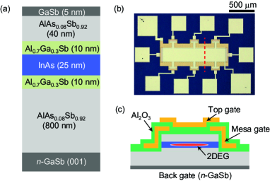
We used a 2DEG formed in an InAs/AlGaSb heterostructure grown by molecular beam epitaxy on an n-type GaSb (001) substrate. Figure 1(a) depicts the layer structure of the wafer. The 2DEG is located in a 25-nm-wide InAs QW sandwiched by 10-nm-thick Al0.7Ga0.3Sb barriers. The QW structure is flanked on both sides by outer AlAs0.08Sb0.92 barrier layers and capped with a 5-nm-thick GaSb. The AlAs0.08Sb0.92 layers were designed to lattice-match the GaSb substrate and thereby suppress dislocation formation. Despite the absence of intentional doping in the structure, electrons are induced in the QW without gate voltages, mainly due to the Fermi level pinning at the GaSb surface Nguyen et al. (1992). The electron density and mobility measured in an ungated sample are m-2 and 118 m2/Vs, respectively. This mobility is comparable to those of recently reported state-of-the-art InAs 2DEGs Shojaei et al. (2016); Tschirky et al. (2017); Hatke et al. (2017); Thomas et al. (2018), attesting to the high quality of our sample.
The heterostructure was processed into a Hall bar with a gate structure designed specifically for this study as shown in Figs. 1(b) and 1(c). In addition to the global top gate and the back gate (n-GaSb substrate), which allow us to independently control the electron density and the electric field across the QW (displacement field), the structure incorporates a third gate (mesa gate), which overlaps only the edge of the mesa and is isolated by atomic-layer-deposited 40-nm-thick Al2O3 layers [Fig. 1(c)]. We electrostatically define the edge of the 2DEG by negatively biasing the mesa gate and depleting the 2DEG underneath Mittag et al. (2018, 2021). This is because in InAs 2DEGs the Fermi level pinning Wieder (2003) and resultant charge accumulation at sample edges can lead to the formation of counterflowing edge channels and destruction of integer quantum Hall effects van Wees et al. (1995); Akiho et al. (2019). We note that similar issues are relevant also in graphene Cui et al. (2016); Marguerite et al. (2019), where the use of an edge-free Corbino structure Zeng et al. (2019); Polshyn et al. (2018) or an electrostatically defined Hall bar Ribeiro-Palau et al. (2019) has been shown to be effective for the observation of fragile FQH states. To ensure the depletion at the mesa edges, we adjusted the voltage applied to the mesa gate for each . The distance between adjacent voltage probes and the width of the Hall bar were 400 and 250 m, respectively. Magnetotransport measurements were carried out at magnetic fields of up to 24 T using a cryogen-free superconducting magnet Awaji et al. (2017) in combination with a 3He refrigerator. The sample was immersed in liquid 3He with the temperature controlled between 0.48–1.52 K. Some additional diagnostic measurements were performed in a dilution refrigerator (base temperature of 13 mK) equipped with a 12 T superconducting magnet. Longitudinal () and transverse () resistances were measured by standard lock-in techniques with ac excitation current of 100 nA at 23 Hz.
III Results and Discussions
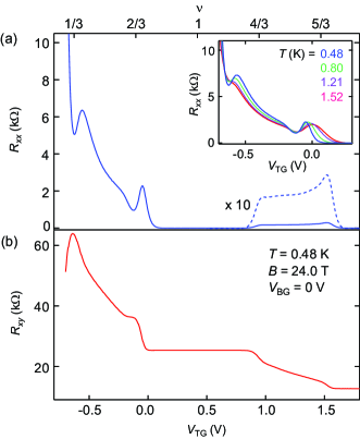
We first show the high-field transport data obtained at V. Figures 2(a) and 2(b) depict and , respectively, measured at 0.48 K by sweeping the top-gate voltage () at T. We observe deep minima in manifesting the FQH effects, at ’s corresponding to and as shown on the top axis. We also observe a plateau in at , but not at , presumably because the 2DEG becomes highly resistive and the Ohmic contacts become poor at low electron density. Interestingly, we see no signatures of FQH states in the region of higher fillings () where the and states are expected. This is not trivial, as mobility generally increases with density.
As shown in the inset of Fig. 2(a), the minima at and are barely temperature dependent for the range studied (0.48–1.52 K). Although not shown, magnetic-field dependent measurements show that the FQH effect is visible only at T, becoming more pronounced with increasing . These results indicate that, at 0.48 K and 24 T, the visibility of the FQH states in our sample is not limited by temperature, but by the disorder present in the sample.
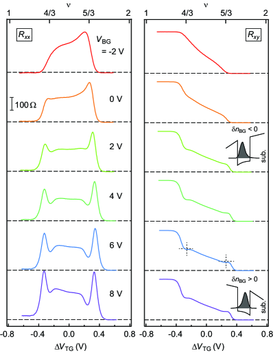
Now we use the back gate to alter the distribution of the electron wave function within the QW and investigate its influence on the FQH states. For this purpose, below we focus on the filling factor region . This is because, at low fillings such as and , the Ohmic contacts did not work properly when a negative was applied. Figure 3 shows the and traces which are taken at T by sweeping at different ’s from to 8 V. The data are plotted as a function of (bottom axis) and (top axis), where represents the change in measured from at each . As increases, minima emerge at and , which become more pronounced with increasing , accompanied by the development of plateaus.
To associate the observed behavior of the FQH effects with the shape of the QW, we need to know at which the QW becomes symmetric. We did this by locating the value for which the second subband becomes occupied at the minimum density at a zero magnetic field. Such an analysis reveals that, for m-2, which corresponds to at 24 T, the QW becomes symmetric at V. Thus, we quantify the asymmetry of the QW by , the electron density added by the back gate with reference to the symmetric point for a given . By taking into account the electron density supplied from the top gate, we find that the QW becomes symmetric at and 5.5 V for and , respectively. The data in Fig. 3 suggest that the FQH states appear as the QW is made progressively symmetric. Interestingly, however, the behavior of the FQH effects is not perfectly symmetric with respect to . This can be seen by comparing the data at and 8 V for and and 8 V for . In both cases, the minimum is more pronounced for the higher , i.e., when the wave function is pushed against the lower, rather than the upper, interface despite the greater asymmetry.
To identify the source of disorder that limits the visibility of the FQH states, we examine the behavior of electron mobility, the most common measure of sample quality. In Fig. 4(a), electron mobility for the constant densities of 2, 4, and m-2 is plotted as a function of . The data show that mobility drops significantly when a large is imposed and the wave function is pushed against the upper or lower InAs/AlGaSb interface. Such a rapid mobility drop is not expected for long-range Coulomb scattering by localized charges. It is also noteworthy that the mobility variation is not symmetric with respect to . The strong dependence suggests that short-range scattering by interface roughness is the dominant contributor. The asymmetry with respect to can then be accounted for by the difference between the upper and lower interfaces.
We have calculated mobility limited by interface-roughness scattering following the method in Ref. Ando (1982). For both interfaces, we started with the parameters reported for InAs/AlGaSb QWs Shojaei et al. (2016), roughness height of nm and correlation length of nm. We then find that, by increasing the roughness height of the lower interface to nm while keeping other parameters the same, the observed asymmetry can be reproduced reasonably well [Fig. 4(a)]. To fit the dependence, one needs to assume an additional scattering mechanism that does not depend on . This -independent contribution used for the fit is plotted in the inset as a function of density. These values agree well with the calculation of mobility limited by background impurities assuming an impurity concentration of cm-3, corroborating that the -independent contribution comes from background-impurity scattering. Calculation using the same interface parameters and reproduces the dependence of mobility on the QW thickness measured for different samples [Fig. 4(b)].
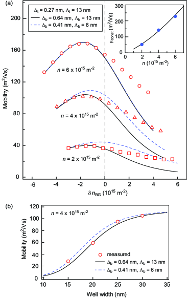
For the fit shown in Fig. 4(a), we chose the parameters to reproduce the behavior near the mobility peak, which unavoidably resulted in the underestimation of mobility at large . This remained true when the correlation length for the lower interface was adjusted as an additional parameter [dashed lines in Fig. 4(a)]. It is known that Sb segregation during growth results in the incorporation of Sb atoms into the InAs layer and causes alloy scattering. Although this could be another source of the asymmetry between positive and negative , we have confirmed that the influence of alloy scattering, calculated for the composition profile reported in Ref. Steinshnider et al. (2000), is negligibly small as compared to interface-roughness scattering. We add that the quantum lifetime evaluated from the low-field Shubnikov-de Haas oscillations was around 0.5 ps, with no significant dependence.
We note that the behavior of the FQH effects is not entirely consistent with the dependence of mobility. For example, upon increasing from to 0 m-2, mobility decreases, whereas the FQH states become better developed. [For (), and 0 m-2 correspond to (2.6) and 4.2 (5.5) V, respectively.] It is known that short-range disorder such as alloy disorder is less detrimental than long-range disorder such as Coulomb scattering on FQH effects Deng et al. (2014); Pan et al. (2011); Betthausen et al. (2014); Kleinbaum et al. (2020). Since interface-roughness scattering is short-ranged in nature, it is not surprising that the stronger roughness scattering on the lower interface does not significantly deteriorate the visibility of the FQH effects. However, it leaves the question of why the FQH effects disappear when the wave function is pushed strongly against the upper interface. One possibility is the potential fluctuation arising from the localized charges trapped at the GaSb/Al2O3 interface. It is known that 2DEG is supplied from the surface states at the semiconductor surface. Our calculation shows that the center of the electron wave function shifts by 6 nm over the range of in Fig. 3. This shift is not negligible as compared to the distance from the upper InAs/AlGaSb interface to the GaSb/Al2O3 interface (55 nm). This implies that the fluctuation in the long-range Coulomb potential that the 2DEG experiences becomes weaker when the wave function shifts toward the lower interface. Although the influence of surface charges on mobility is minor, their impact on FQH effects may not be negligible. This is similar to the case of remote ionized impurities in modulation-doped GaAs/AlGaAs heterostructures or QWs, where their impact on FQH effects is significant even when their influence on mobility is minor Gamez and Muraki (2013).
It is worth mentioning that the InAs 2DEG samples used in most studies, including ours, are undoped, where the electrons are induced by the Fermi-level pinning at the semiconductor surface Nguyen et al. (1992). Our study suggests that the surface charge may affect the visibility of the FQH effects, which could be a reason why FQH effects are not readily observable in InAs 2DEGs in spite of the high electron mobility. One way to mitigate this might be to increase the distance from the surface to the 2DEG. This would inevitably reduce the electron density, which could neverthless be compensated by using a front or back gate as we partially demonstrated here. It should be also mentioned that in this study we used a specially designed Hall bar, in which the edges of the 2DEG were electrostatically defined by gates. If the physical edges of the sample are to be used, one would need to take care to avoid the influence from the possible charge accumulation at the edges van Wees et al. (1995); Akiho et al. (2019), which may affect FQH effects. Lastly, we must note that the high mobility in InAs/AlGaSb QWs is partly due to the small effective mass in InAs; even in high-quality samples, the background impurity concentration (a few 1015 cm-3) is still much higher than in GaAs/AlGaAs samples of moderate quality (a few 1014 cm-3). It is therefore essential to further improve the crystal quality to realize FQH effects at lower magnetic fields compatible with superconductivity.
IV Summary
We have observed FQH effects at , , , and in an InAs 2DEG using a dual-gated Hall bar with gate-defined edges. We demonstrated that the shape of the QW confinement potential has a significant impact on the visibility of the FQH states. Comparison with the variation of zero-field electron mobility suggests an additional source of disorder, other than interface roughness and background impurities, that affects the FQH effects. Our results hint at the need to further optimize the heterostructure design, in addition to improving crystal quality, for the realization of robust FQH states in InAs.
Acknowledgments
The authors thank Hiroaki Murofushi for device fabrication, Miki Imai for constructing measurement setups, and Norio Kumada for discussions and useful comments on the manuscript. High-field measurements were performed at the High Field Laboratory for Superconducting Materials, Institute for Materials Research, Tohoku University (Project No. 20H0066).
S.K. and H.I. contributed equally to this work.
References
- Clarke et al. (2013) D. J. Clarke, J. Alicea, and K. Shtengel, “Exotic non-Abelian anyons from conventional fractional quantum Hall states,” Nat. Commun. 4, 1348 (2013).
- Clarke et al. (2014) D. J. Clarke, J. Alicea, and K. Shtengel, “Exotic circuit elements from zero-modes in hybrid superconductor-quantum-Hall systems,” Nat. Phys. 10, 877 (2014).
- Mong et al. (2014) R. S. K. Mong, D. J. Clarke, J. Alicea, N. H. Lindner, P. Fendley, C. Nayak, Y. Oreg, A. Stern, E. Berg, K. Shtengel, and M. P. A. Fisher, “Universal Topological Quantum Computation from a Superconductor-Abelian Quantum Hall Heterostructure,” Phys. Rev. X 4, 011036 (2014).
- (4) Ö. Gül, Y. Ronen, S. Y. Lee, H. Shapourian, J. Zauberman, Y. H. Lee, K. Watanabe, T. Taniguchi, A. Vishwanath, A. Yacoby, and P. Kim, “Andreev reflection in the fractional quantum Hall state,” arXiv:2009.07836 .
- Kjaergaard et al. (2016) M. Kjaergaard, F. Nichele, H. J. Suominen, M. P. Nowak, M. Wimmer, A. R. Akhmerov, J. A. Folk, K. Flensberg, J. Shabani, C. J. Palmstrøm, and C. M. Marcus, “Quantized conductance doubling and hard gap in a two-dimensional semiconductor-superconductor heterostructure,” Nat. Commun. 7, 12841 (2016).
- Shojaei et al. (2016) B. Shojaei, A. C. C. Drachmann, M. Pendharkar, D. J. Pennachio, M. P. Echlin, P. G. Callahan, S. Kraemer, T. M. Pollock, C. M. Marcus, and C. J. Palmstrøm, “Limits to mobility in InAs quantum wells with nearly lattice-matched barriers,” Phys. Rev. B 94, 245306 (2016).
- Tschirky et al. (2017) T. Tschirky, S. Mueller, Ch. A. Lehner, S. Fält, T. Ihn, K. Ensslin, and W. Wegscheider, “Scattering mechanisms of highest-mobility quantum wells,” Phys. Rev. B 95, 115304 (2017).
- Hatke et al. (2017) A. T. Hatke, T. Wang, C. Thomas, G. C. Gardner, and M. J. Manfra, “Mobility in excess of 106 cm2/V s in InAs quantum wells grown on lattice mismatched InP substrates,” Appl. Phys. Lett. 111, 142106 (2017).
- Thomas et al. (2018) C. Thomas, A. T. Hatke, A. Tuaz, R. Kallaher, T. Wu, T. Wang, R. E. Diaz, G. C. Gardner, M. A. Capano, and M. J. Manfra, “High-mobility InAs 2DEGs on GaSb substrates: A platform for mesoscopic quantum transport,” Phys. Rev. Materials 2, 104602 (2018).
- Ma et al. (2017) M. K. Ma, Md. S. Hossain, K. A. Villegas Rosales, H. Deng, T. Tschirky, W. Wegscheider, and M. Shayegan, “Observation of fractional quantum Hall effect in an InAs quantum well,” Phys. Rev. B 96, 241301(R) (2017).
- Nguyen et al. (1992) C. Nguyen, B. Brar, H. Kroemer, and J. H. English, “Surface donor contribution to electron sheet concentrations in not-intentionally doped InAs-AlSb quantum wells,” Appl. Phys. Lett. 60, 1854 (1992).
- Mittag et al. (2018) C. Mittag, M. Karalic, Z. Lei, T. Tschirky, W. Wegscheider, T. Ihn, and K. Ensslin, “Edgeless and purely gate-defined nanostructures in InAs quantum wells,” Appl. Phys. Lett. 113, 262103 (2018).
- Mittag et al. (2021) C. Mittag, J. V. Koski, M. Karalic, C. Thomas, A. Tuaz, A. T. Hatke, G. C. Gardner, M. J. Manfra, J. Danon, T. Ihn, and K. Ensslin, “Few-Electron Single and Double Quantum Dots in an Two-Dimensional Electron Gas,” PRX Quantum 2, 010321 (2021).
- Wieder (2003) H. H. Wieder, “Surface and interface barriers of InxGa1-xAs binary and ternary alloys,” J. Vac. Sci. Technol. B 21, 1915 (2003).
- van Wees et al. (1995) B. J. van Wees, G. I. Meijer, J. J. Kuipers, T. M. Klapwijk, W. van de Graaf, and G. Borghs, “Breakdown of the quantum Hall effect in InAs/AlSb quantum wells due to counterflowing edge channels,” Phys. Rev. B 51, 7973 (1995).
- Akiho et al. (2019) T. Akiho, H. Irie, K. Onomitsu, and K. Muraki, “Counterflowing edge current and its equilibration in quantum Hall devices with sharp edge potential: Roles of incompressible strips and contact configuration,” Phys. Rev. B 99, 121303(R) (2019).
- Cui et al. (2016) Y.-T. Cui, B. Wen, E. Y. Ma, G. Diankov, Z. Han, F. Amet, T. Taniguchi, K. Watanabe, D. Goldhaber-Gordon, C. R. Dean, and Z.-X. Shen, “Unconventional Correlation between Quantum Hall Transport Quantization and Bulk State Filling in Gated Graphene Devices,” Phys. Rev. Lett. 117, 186601 (2016).
- Marguerite et al. (2019) A. Marguerite, J. Birkbeck, A. Aharon-Steinberg, D. Halbertal, K. Bagani, I. Marcus, Y. Myasoedov, A. K. Geim, D. J. Perello, and E. Zeldov, “Imaging work and dissipation in the quantum Hall state in graphene,” Nature 575, 628 (2019).
- Zeng et al. (2019) Y. Zeng, J. I. A. Li, S. A. Dietrich, O. M. Ghosh, K. Watanabe, T. Taniguchi, J. Hone, and C. R. Dean, “High-Quality Magnetotransport in Graphene Using the Edge-Free Corbino Geometry,” Phys. Rev. Lett. 122, 137701 (2019).
- Polshyn et al. (2018) H. Polshyn, H. Zhou, E. M. Spanton, T. Taniguchi, K. Watanabe, and A. F. Young, “Quantitative Transport Measurements of Fractional Quantum Hall Energy Gaps in Edgeless Graphene Devices,” Phys. Rev. Lett. 121, 226801 (2018).
- Ribeiro-Palau et al. (2019) R. Ribeiro-Palau, S. Chen, Y. Zeng, K. Watanabe, T. Taniguchi, J. Hone, and C. R. Dean, “High-Quality Electrostatically Defined Hall Bars in Monolayer Graphene,” Nano Lett. 19, 2583 (2019).
- Awaji et al. (2017) S. Awaji, K. Watanabe, H. Oguro, H. Miyazaki, Sa. Hanai, T. Tosaka, and S. Ioka, “First performance test of a 25 T cryogen-free superconducting magnet,” Supercond. Sci. Technol. 30, 065001 (2017).
- Ando (1982) T. Ando, “Self-Consistent Results for a GaAs/AlxGa1-xAs Heterojunciton. II. Low Temperature Mobility,” J. Phys. Soc. Jpn. 51, 3900 (1982).
- Steinshnider et al. (2000) J. Steinshnider, J. Harper, M. Weimer, C.-H. Lin, S. S. Pei, and D. H. Chow, “Origin of Antimony Segregation in Strained-Layer Superlattices,” Phys. Rev. Lett. 85, 4562 (2000).
- Deng et al. (2014) N. Deng, G. C. Gardner, S. Mondal, E. Kleinbaum, M. J. Manfra, and G. A. Csáthy, “ Fractional Quantum Hall State in the Presence of Alloy Disorder,” Phys. Rev. Lett. 112, 116804 (2014).
- Pan et al. (2011) W. Pan, N. Masuhara, N. S. Sullivan, K. W. Baldwin, K. W. West, L. N. Pfeiffer, and D. C. Tsui, “Impact of Disorder on the Fractional Quantum Hall State,” Phys. Rev. Lett. 106, 206806 (2011).
- Betthausen et al. (2014) C. Betthausen, P. Giudici, A. Iankilevitch, C. Preis, V. Kolkovsky, M. Wiater, G. Karczewski, B. A. Piot, J. Kunc, M. Potemski, T. Wojtowicz, and D. Weiss, “Fractional quantum Hall effect in a dilute magnetic semiconductor,” Phys. Rev. B 90, 115302 (2014).
- Kleinbaum et al. (2020) E. Kleinbaum, H. Li, N. Deng, G. C. Gardner, M. J. Manfra, and G. A. Csáthy, “Disorder broadening of even-denominator fractional quantum Hall states in the presence of a short-range alloy potential,” Phys. Rev. B 102, 035140 (2020).
- Gamez and Muraki (2013) G. Gamez and K. Muraki, “ fractional quantum Hall state in low-mobility electron systems: Different roles of disorder,” Phys. Rev. B 88, 075308 (2013).