Disentangling cathodoluminescence spectra in nanophotonics: particle eigenmodes vs transition radiation
Abstract
Cathodoluminescence spectroscopy performed in an electron microscope has proven a versatile tool for analysing the near- and far-field optical response of plasmonic and dielectric nanostructures. Nevertheless, the transition radiation produced by electron impact is often disregarded in the interpretation of the spectra recorded from resonant nanoparticles. Here we show, experimentally and theoretically, that transition radiation can by itself generate distinct resonances which, depending on the time of flight of the electron beam inside the particle, can result from constructive or destructive interference in time. Superimposed on the eigenmodes of the investigated structures, these resonances can distort the recorded spectrum and lead to potentially erroneous assignment of modal characters to the spectral features. We develop an intuitive analogy that helps distinguish between the two contributions. As an example, we focus on the case of silicon nanospheres, and show that our analysis facilitates the unambiguous interpretation of experimental measurements on Mie-resonant nanoparticles.
keywords:
Cathodoluminescence, electron-beam spectroscopy, dielectric nanoparticles, Mie resonances, mode characterisation, transition radiationSDU] Center for Nano Optics, University of Southern Denmark, Campusvej 55, DK-5230 Odense M, Denmark \alsoaffiliation[equal] These two authors contributed equally to the paper SDU] Center for Nano Optics, University of Southern Denmark, Campusvej 55, DK-5230 Odense M, Denmark \alsoaffiliation[equal] These two authors contributed equally to the paper DTU] Department of Physics, Technical University of Denmark, Fysikvej, DK-2800 Kongens Lyngby, Denmark \alsoaffiliation[SDU] Center for Nano Optics, University of Southern Denmark, Campusvej 55, DK-5230 Odense M, Denmark SDU] Center for Nano Optics, University of Southern Denmark, Campusvej 55, DK-5230 Odense M, Denmark Kobe] Department of Electrical and Electronic Engineering, Kobe University, Rokkodai, Nada, Kobe 657-8501, Japan Kobe] Department of Electrical and Electronic Engineering, Kobe University, Rokkodai, Nada, Kobe 657-8501, Japan SDU] Center for Nano Optics, University of Southern Denmark, Campusvej 55, DK-5230 Odense M, Denmark \alsoaffiliation[DIAS] Danish Institute for Advanced Study, University of Southern Denmark, Campusvej 55, DK-5230 Odense M, Denmark DTU] Department of Physics, Technical University of Denmark, Fysikvej, DK-2800 Kongens Lyngby, Denmark SDU] Center for Nano Optics, University of Southern Denmark, Campusvej 55, DK-5230 Odense M, Denmark {tocentry}
![[Uncaptioned image]](/html/2112.04931/assets/x1.png)
Electron-based microscopy techniques that harness signals generated from the excitation of a material by a fast electron beam have proven essential for exploring the optical properties of matter 1, 2, offering one of the most efficient platforms for achieving subwavelength-resolution imaging 3. They combine the possibility of spatial resolution optimisation 4 with efficient specimen excitation 5, and have met with growing popularity in quantum- and nano-optics, e.g. to study semiconductor nanowires 6, quantum dots 7, 8, 9 or quantum confinement 10, 11 and to image plasmons 12, 13. Depending on signal nature and detection process, electron microscopy and spectroscopy come in different flavours, such as electron energy-loss spectroscopy (EELS) and scanning electron microscopy (SEM) 2. Among these, cathodoluminescence (CL) spectroscopy, which collects the light emitted by the interaction of the electron beam with the sample, allows direct imaging of optical modes in plasmonic 14, 15 or dielectric 16 nanoparticles (NPs), while enabling detection of optically dark excitations 5, visualisation of the local density of optical states 17, 18, 19, or even tomographic reconstruction of the optical near fields 20. These successful endeavours have led to increasingly extended use of CL spectroscopy as a principal method for analysing photonic nanostructures, including the characterisation of plasmonic 21 or Mie-resonant dielectric NPs 22.
Despite this success, particular care must be taken when interpreting CL measurements, since the recorded signal can originate from either excitation of eigenmodes or directly from transition radiation (TR) 23, 24, 25. Here, we demonstrate how, in the case of electron beams traversing NPs, the presence of resonances resulting from interfering TR emanating from the two NP sides with a time delay has the potential to hinder the unambiguous interpretation of measured spectra in terms of NP eigenmodes. The two competing mechanisms are, in principle, present in any CL experiment —albeit sometimes too weak to observe, depending on the sample— and can lead to large discrepancies between anticipated and observed frequencies of NP resonances. We show that this behaviour is particularly relevant when the electron beam penetrates the NP near its centre and/or with low velocity, so that its time of flight in the NP is maximal, and provide an intuitive theoretical description based on the time delay between the consecutive excitation of radiating dipoles at the entering and exiting surfaces of the NP. While recent works have indeed proved CL a powerful tool in the study, design and monitoring of both dielectric- and plasmonic-based nanostructures 26, 27, 28, 29, 30, 31, most experiments and analyses have focused on relatively small NPs and non-penetrating electron beams accelerated at as high a voltage as possible (so as to excite NP resonances more efficiently while limiting the electron beam spreading), and the emergence of additional interference mechanisms for penetrating beams —and the possible complications that accompany it— has remained unexplored.
In what follows, we choose to analyse the emission properties of Si NPs, because of their high refractive index and low Ohmic losses 32, the multitude of co-existing modes in the visible 33, 34 —with the field largely confined inside the NP, thus calling for traversing electron beams— and the relatively large sizes required for the full glory of all Mie resonances to unveil itself 35; the combination of these features can significantly pronounce the interference effects under study. The spectra of Mie-resonant NPs are characterised by multipoles of both electric and magnetic character 36, Fano resonances 37, anapoles 38, and bound states in the continuum 39, and have enabled functionalities as diverse as directional light scattering 40, 41 and emission 42, directional couplers 43, 44, and Huygens-based metasurfaces 45, 46. All-dielectric nanodevices are thus proposed as promising alternatives to plasmonics, with possible applications in biosensing 47, 48, nanoantennas 49, 50, slow light 51, thermo-optic tuning 52, ultra-violet interband plasmonics 53, fluorescence control 54, 55, 56, and Mie-exciton strong-coupling 57, 58, 59, 60.
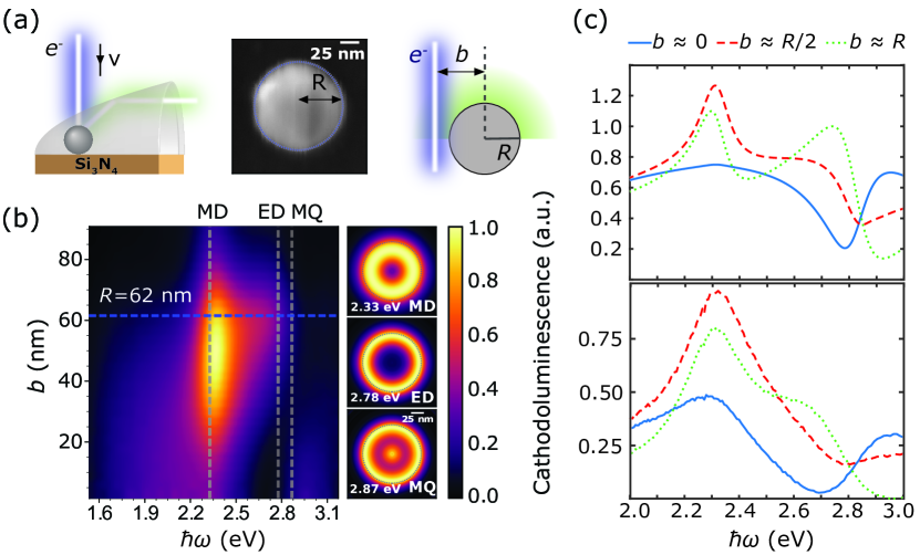
CL measurements are performed with the set-up shown schematically in the left-hand sketch of Figure 1a (see Methods for details). Si nanospheres of radius (prepared in an agglomeration-free colloidal solution 61; typical SEM image is shown in the middle panel of the figure), placed on a thin Si3N4 membrane, are exposed to swift electrons travelling at velocity (with a corresponding relativistic factor , where is the speed of light in vacuum), for different impact parameters (see right-hand schematic of Figure 1a), corresponding to either non-penetrating or penetrating electron beams. The colour map of Figure 1b shows experimental CL spectra for a relatively small NP ( nm) —for which modal characters should be straightforward to assign— as a function of impact parameter. Vertical dashed lines indicate the energies where different multipoles are predicted by standard Mie theory 55 for this NP size (for extinction spectra and their multipolar decomposition, see Supporting Information). Two resonances manifest clearly in the spectra for large impact parameters: a sharp magnetic dipole (MD) at about eV, and a broader and less intense electric dipole (ED) around eV. A magnetic quadrupole (MQ) is identified in the extinction spectra as a weak contribution to the total extinction at about eV, but it is hardly discernible in CL due to losses and its short lifetime. These features are in good agreement with corresponding dark-field spectra from literature 36, but this agreement becomes worse for small impact parameters, close to the NP centre. Differences between theoretical extinction and experimental CL spectra might initially be attributed to NP shape imperfections and the presence of the thin substrate 62, 63, but this turns out to be only a minor source of deviations, as we discuss below. To better illustrate the nature of the various resonances, in Figure 1b we also show experimental CL maps at the three energies analysed above.
To further analyse the CL spectra, and in order to identify if and where theoretical extinction calculations fail to interpret the measurements, we compare in Figure 1c experimental spectra (lower panel) with exact analytic Mie-theory based CL calculations 22 (equivalent to the standard Mie theory for plane-wave excitation, see Methods), for three characteristic impact parameters: a grazing electron beam (, green dotted lines), a penetrating beam passing halfway between the edge and centre of the NP (, red dashed lines), and one passing exactly through the centre (note that the theoretical calculations are performed for a small nm for convergence reasons; in any case, this is within the experimental electron-beam diameter). Different impact parameters are expected to excite different modes with different weights, while TR-related signals also become relevant when penetrating beams are considered. Indeed, as the electron beam approaches the centre, the MD is less efficiently excited for symmetry reasons; in theory, for the MD contribution should be exactly zero, but in practice the electron beam does not follow strictly a straight line (see Supporting Information for Monte Carlo maps of the electron trajectories). At the same time, the ED seems to shift in energy as changes, while even stronger shifts are exhibited by the dip at about eV, identified as an anapole 16. These shifts are not justified by the poles of the corresponding Mie coefficients (where eigenmodes are located), and their origin is the main focus of the remainder of this paper.
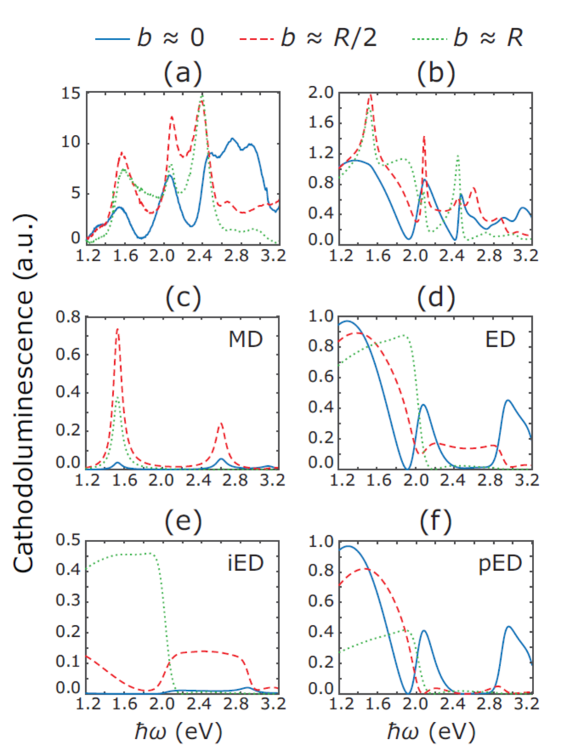
The spectra of Figure 1c already suggest that a multipolar decomposition in terms of Mie coefficients might not be straightforward. To better analyse the situation we shift in Figure 2 our attention to a larger NP with nm, where higher-order multipoles are expected to contribute significantly (see corresponding extinction in the Supporting Information). The MD and ED modes have now moved to lower energies due to retardation, and additional higher-order multipoles are clearly visible in the CL spectra at higher energies (above eV), in both experimental (Figure 2a) and theoretical (Figure 2b) spectra, while the agreement between measurements and calculations becomes more questionable, especially regarding the relative peak intensities. For example, the sharp peak at about eV for in Figure 2b can be attributed to an electric quadrupole, but it is not clear why its intensity in Figure 2a is so much larger. It is noteworthy that both the resonance peaks and the dips change intensities and positions as the impact parameter varies. To assign a multipolar character to such rich spectra, the most natural approach is to use Mie theory (in its electron-beam incarnation) to decompose them into independent contributions. Indeed, in Figure 2c the MD resonance at about eV becomes weaker as the electron-beam trajectory approaches the NP centre, while remaining practically fixed in energy, as expected. At the same time, one can observe at higher energies, around eV, the emergence of the first radial MD 16. On the other hand, the ED contribution shown in Figure 2d is not straightforward to interpret: it appears as if the main (first-order radial) ED keeps redshifting away from the actual pole of the scattering coefficient (see Methods) as the electron beam approaches the centre, while additional resonances that cannot be attributed to radial EDs appear in the energy window eV. Some kind of plateau is also visible between and eV, which is probably related to the large width of the ED, combined with what is known as interference structure due to size in large NPs 64. This peculiar response is better illustrated in Figures 2e-f, where the ED spectrum is further decomposed into in-plane (iED, plane normal to the electron beam and parallel to the substrate in the experiment) and perpendicular (pED, normal to the substrate) EDs —since the electric field of the electron beam has non-negligible components in all directions, it can excite both kinds of dipolar modes. The most striking feature is the strong shift (from to eV for the lowest-energy resonance), accompanied by an increase in intensity, and the oscillatory response of all resonances in the case of the pED shown in Figure 2f. There is practically no mechanism that could shift an ED to such an extent just by changing the impact parameter (the pole of the corresponding scattering matrix is at about eV). Nevertheless, these oscillations are reminiscent of the transition radiation manifestation discussed by Pogorzelski and Yeh 23, which (for ) is characterised by a dependence
| (1) |
for the low (below the Cherenkov limit, as we discuss next) electron velocities and the dipolar modes of interest here. Note that the argument is originally expressed in terms of the wavenumber (rather than the angular frequency ) and the velocity of the electron in the NP, both containing its refractive index so that it eventually cancels out. In what follows, we show that this response emerges from the interference of the TR emitted from the two points where the electron beam crosses the NP surface (the same TR that is responsible for the excitation of Mie modes) with the time delay required for the electron to traverse the NP from top to bottom, becoming stronger as the electron beam approaches the NP centre and the electron time of flight increases.
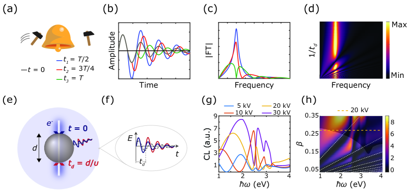
To obtain an intuitive understanding of the effects discussed above, let us first focus on the classical analogue analysed in Figures 3a-d. Figure 3a shows a bell which, at time , is hit by a hammer on its left side, generating an acoustic wave in the far field, with period . A second hammer hits the bell on the opposite side, with some time delay . The amplitudes of the first acoustic wave (grey line), and the three different superpositions of initial plus delayed wave are shown as a function of time in Figure 3b, where we plot three different time delays for the second signal, corresponding to (blue line), (red line), and (green line) —naturally, all waves decay in time. In Figure 3c we plot the Fourier transform (FT) of the total wave that reaches an observer (in this case listener). The frequency-domain signal displays an oscillatory behaviour, with zero amplitude emerging whenever the conditions for destructive interference are met. The amplitude colour map of Figure 3d shows, for each time delay, where destructive interference dips at different frequencies are expected, superimposed over the natural Lorentzian frequency of the oscillator; a linear dependence between the inverse of the time delay and the frequency is predicted.
The same concept can equally well apply to the case of NPs excited by a penetrating electron beam. Thinking of the beam as one electron approaching the NP at a time, an image charge appears inside the NP, leading to the formation of an electric dipole. As the electron approaches the surface, so does the image charge 65, 66, 24 until, at contact, the two charges collapse, resulting in TR (Figure 3e). This collapse also occurs at the bottom side of the particle, with a time delay (where is the electron path length in the NP). The two dipoles can interfere constructively or destructively, depending on the time delay of their emergence which, in turn, depends on the factors that determine the time of flight: and . This response can, in principle, be expected for any NP shape and can be studied analytically 67 or numerically 68; it should be noted, however, that the spherical shape stresses the effect, because the electron beam exits the NP at an interface with air, and collecting the resulting radiation might be easier. The corresponding temporal oscillations (red and blue lines), together with an NP Mie resonance (dashed grey line) are sketched in Figure 3f. Exact calculations of CL spectra for different acceleration voltages (corresponding to different electron velocities) are shown in Figure 3g, in the range kV, which is experimentally feasible. For low voltages (see, e.g., the blue line for kV) the only recorded signal originates from TR. As the electron beam is further accelerated, the modes of the NP are more efficiently excited, leading to CL signals that emerge as a superposition of NP resonances and interfering TR. This complex interaction is displayed more clearly in the CL colour map of Figure 3h where, in addition to the linear response of the interference dips, one can see for higher electron velocities slight anticrossings when the NP Mie resonances are met. The differently-shaded upper part of Figure 3h marks the velocity/energy window in which the Cherenkov-radiation condition (with being the NP permittivity) is met. While, by simply looking at this, one could at first think that Cherenkov radiation plays an important role in the final form of the measured CL spectra, in the Supporting Information we show that this is not the case; its only manifestation in Figure 3h is the bright feature for at eV. The overall behaviour of the CL spectra suggests thus that CL minima are extremely sensitive to TR, and care must be taken so as not to assign to such dips an anapole character before further verification. Furthermore, the uneven spectral excitation implies that, even at high acceleration voltages, observed peaks may be noticeably shifted away from the natural Mie resonances, which must be kept in mind when interpreting CL measurements.

To verify our explanation, and indeed prove that TR interference can be observed in experiments with small NPs (as in the case of thin films 69, 70, 71, where Fabry–Pérot interference emerges due to multiple reflections) and affect the final spectra, we record in Figure 4 the CL spectra of a Si sphere with nm at different acceleration voltages, for an electron beam passing through the NP centre (). The spectra are affected by the fact that the electron trajectories are in practice not straight, because the electron mean free path is just few tens of nm, and the electrons undergo inelastic scattering before exiting the NP 72 (see Supporting Information for corresponding Monte Carlo simulations for low and higher acceleration voltages), thus leading to both inhomogeneous broadening due to interference events occurring with different time delays, and to non-negligible contribution from MD terms. Nevertheless, traces of the oscillations related to TR can indeed be identified. This is better seen in the spectum for kV, which exhibits four resonances at , , and eV, whereas extinction calculations only predict an MD at about eV and an ED/MQ at about eV; the other two resonances can be attributed to TR interference or, possibly, Cherenkov radiation (in the eV case), and the energies of the dips are in excellent agreement with the predictions of Figure 3h (see yellow horizontal line in that figure). The most remarkable feature is the behaviour of the energy dip at eV for high acceleration voltage ( kV); as the voltage decreases, this dip transforms into a peak at the same energy (see red markers), with no correspondence to any NP eigenmode. Similarly, the shoulder around eV observed at kV, which disappears for voltages below kV, also does not correspond to any pole of the scattering matrix of the NP. The above discussion finally sheds more light on the spectra of Figure 1c; for external beams, two Mie resonances are observed at eV and eV, while no traces of TR are present. On the contrary, for penetrating beams, and particularly when the beam crosses the centre and some of the Mie modes are inactive for symmetry reasons, it is TR that dominates the spectra.
Conclusions
In summary, we identified TR in CL measurements as a possible source of interference with NP resonances, leading to ambiguous, possibly erroneous, assignment of modal characters to spectral features. When penetrating electron beams are used, two radiating dipoles are formed when the electron and its image charge collapse at the two opposite NP surfaces, with a time delay that is related to the velocity of the electron and the length of its path inside the NP. These two parameters define whether the interference of the two dipoles will be constructive, leading to pronounced resonances that can mask those due to the NP, or destructive, leading to dips reminiscent of anapoles, but not necessarily of that nature. Care must thus be taken in the interpretation of CL measurements, especially when characterisation of NP properties is at question. To avoid these effects, one can always choose to analyse external electron beams only, or use as high an acceleration voltage as possible, while the interference will probably be less pronounced if the shape of the NP and its positioning are such that the exiting radiating dipole is formed at the interface with the substrate.
Methods
Cathodoluminescence spectroscopy
CL spectroscopy is performed in a Tescan Mira3 scanning electron microscope operated at an acceleration voltage ranging from kV to kV, current of pA, and corresponding spot sizes between nm and nm. Light emitted from the sample is collected by a parabolic mirror and analysed using a Delmic SPARC CL detector equipped with an Andor Newton CCD camera. All CL spectra are corrected for the system response and the background of the thin Si3N4 membrane. Here, the almost negligible background emission of the substrate, collected at an unexposed position close to the studied Si NP, is subtracted from the sample signal and subsequently divided by the correction curve of the total system response (recorded separately). All experimental CL spectra in this work correspond to (relative) photon intensity per wavelength interval, subsequently converted to energy, taking into account the monochromator dispersion: , where is the wavelength. Therefore, the recorded CL intensity is multiplied with . All CL maps are collected with activated sub-pixel scanning.
In the case of the CL colour map shown in Figure 1b, the spectrum is integrated over separate spatial ranges from to with a step of . It should be noted that the spectrum which is used for the background subtraction, in this case, is a signal collected by the spectrometer with a blanked electron beam. Using a linear interpolation we produce the data for evenly spaced energy points with the largest energy separation of eV and apply a Gaussian filter with standard deviation eV. Finally, we plot the resulting spectra as a colour map. The CL maps of different Mie modes shown in Figure 1b are plotted for energy-scale converted CL signal integrated over the wavelength range of nm centred at the resonance energy. We utilise the spherical symmetry of the Si NPs to radially integrate the signal located at the same distance from the particle centre and show it as a two-dimensional map.
Analytic CL calculation
The analytic theory for the interaction of spherical NPs with fast electron beams has been developed by García de Abajo 26, 1, 22; here and in the Supporting Information we only highlight the key points for completeness. The angle-integrated photon emission probability in the interaction of a Si sphere (described here by the experimental values of Green 73) with an electron beam passing at impact parameter with constant velocity is described by the expression 22
| (2) |
where is the elementary charge, is the speed of light in vacuum, the vacuum permittivity and the photon energy. The summation over includes electric () and magnetic () multipoles, characterised by the angular momentum numbers and . Analytic expressions for the coefficients are provided in the Supporting Information; they describe the expansion of the field of a moving electron into spherical waves, for the two different regions (inside and outside the NP).
S. R. is a Sapere Aude research leader supported by Independent Research Fund Denmark (Grant No. 7026-00117B). N. A. M. is a VILLUM Investigator supported by VILLUM FONDEN (Grant No. 16498). C. W. acknowledges funding from a MULTIPLY fellowship under the Marie Skłodowska-Curie COFUND Action (Grant agreement No. 713694). P. E. S. is the recipient of the Zonta Denmark’s Scholarship for female PhD students in Science and Technology 2021.
Details about the analytic CL calculation; Mie-theory extinction spectra; Monte Carlo simulations of electron trajectories, Sample degradation test.
References
- García de Abajo 2010 García de Abajo, F. J. Optical excitations in electron microscopy. Rev. Mod. Phys. 2010, 82, 209–275
- Polman et al. 2019 Polman, A.; Kociak, M.; García de Abajo, F. J. Electron-beam spectroscopy for nanophotonics. Nat. Mater. 2019, 18, 1158–1171
- Lazar et al. 2006 Lazar, S.; Botton, G. A.; Zandbergen, H. W. Enhancement of resolution in core-loss and low-loss spectroscopy in a monochromated microscope. Ultramicroscopy 2006, 106, 1091–1103
- García de Abajo and Di Giulio 2021 García de Abajo, F. J.; Di Giulio, V. Optical excitations with electron beams: challenges and opportunities. ACS Photonics 2021, 8, 945–974
- Koh et al. 2009 Koh, A. L.; Bao, K.; Khan, I.; Smith, W. E.; Kothleitner, G.; Nordlander, P.; Maier, S. A.; McComb, D. W. Electron energy-loss spectroscopy (EELS) of surface plasmons in single silver nanoparticles and dimers: influence of beam damage and mapping of dark modes. ACS Nano 2009, 3, 3015–3022
- Yamamoto et al. 2006 Yamamoto, N.; Bhunia, S.; Watanabe, Y. Polarized cathodoluminescence study of InP nanowires by transmission electron microscopy. Appl. Phys. Lett. 2006, 88, 153106
- Grundmann et al. 1995 Grundmann, M.; Christen, J.; Ledentsov, N. N.; Böhrer, J.; Bimberg, D.; Ruvimov, S. S.; Werner, P.; Richter, U.; Gösele, U.; Heydenreich, J.; Ustinov, V. M.; Egorov, A. Y.; Zhukov, A. E.; Kop’ev, P. S.; Alferov, Z. I. Ultranarrow luminescence lines from single quantum dots. Phys. Rev. Lett. 1995, 74, 4043–4046
- Rodt et al. 2005 Rodt, S.; Schliwa, A.; Pötschke, K.; Guffarth, F.; Bimberg, D. Correlation of structural and few-particle properties of self-organized InAs/GaAS quantum dots. Phys. Rev. B 2005, 71, 155325
- Mahfoud et al. 2013 Mahfoud, Z.; Dijksman, A. T.; Javaux, C.; P., B.; Baudrion, A.-L.; Plain, J.; Dubertret, B.; Kociak, M. Cathodoluminescence in a scanning transmission electron microscope: a nanometer-scale counterpart of photoluminescence for the study of II-VI quantum dots. J. Phys. Chem. Lett. 2013, 4, 4090– 4094
- Grundmann et al. 1989 Grundmann, M.; Christen, J.; Bimberg, D.; Fischer-Colbrie, A.; Hull, R. Misfit dislocations in pseudomorphic In0.23Ga0.77As/GaAs quantum wells: influence on lifetime and diffusion of excess excitons. J. Appl. Phys. 1989, 66, 2214–2216
- Zagonel et al. 2011 Zagonel, L. F.; Mazzucco, S.; Tencé, M.; March, K.; Bernard, R.; Laslier, B.; Jacopin, G.; Tchernycheva, M.; Rigutti, L.; Julien, F. H.; Songmuang, R.; Kociak, M. Nanometer scale spectral imaging of quantum emitters in nanowires and its correlation to their atomically resolved structure. Nano Lett. 2011, 11, 568–573
- Yamamoto et al. 2001 Yamamoto, N.; Araya, K.; García de Abajo, F. J. Photon emission from silver particles induced by a high-energy electron beam. Phys. Rev. B 2001, 64, 205419
- Vesseur et al. 2007 Vesseur, E. J. R.; de Waele, R.; Kuttge, M.; Polman, A. Direct observation of plasmonic modes in Au nanowires using high-resolution cathodoluminescence spectroscopy. Nano Lett. 2007, 7, 2843–2846
- Chaturvedi et al. 2009 Chaturvedi, P.; Hsu, K. H.; Kumar, A.; Fung, K. H.; Mabon, J. C.; Fang, N. X. Imaging of plasmonic modes of silver nanoparticles using high-resolution cathodoluminescence spectroscopy. ACS Nano 2009, 3, 2965–2974
- Sannomiya et al. 2020 Sannomiya, T.; Konečná, A.; Matsukata, T.; Thollar, Z.; Okamoto, T.; García de Abajo, F. J.; Yamamoto, N. Cathodoluminescence phase extraction of the coupling between nanoparticles and surface plasmon polaritons. Nano Lett. 2020, 20, 592–598
- Matsukata et al. 2019 Matsukata, T.; Matthaiakakis, N.; Yano, T.; Hada, M.; Tanaka, T.; Yamamoto, N.; Sannomiya, T. Selection and visualization of degenerate magnetic and electric multipoles up to radial higher orders by cathodoluminescence. ACS Photonics 2019, 6, 2320–2326
- García de Abajo and Kociak 2008 García de Abajo, F. J.; Kociak, M. Probing the photonic local density of states with electron energy loss spectroscopy. Phys. Rev. Lett. 2008, 100, 106804
- Sapienza et al. 2012 Sapienza, R.; Coenen, T.; Renger, J.; Kuttge, M.; van Hulst, N. F.; Polman, A. Deep-subwavelength imaging of the modal dispersion of light. Nat. Mater. 2012, 11, 781–787
- Zu et al. 2019 Zu, S.; Han, T.; Jiang, M.; Liu, Z.; Jiang, Q.; Lin, F.; Zhu, X.; Fang, Z. Imaging of plasmonic chiral radiative local density of states with cathodoluminescence nanoscopy. Nano Lett. 2019, 19, 775–780
- Atre et al. 2015 Atre, A. C.; Brenny, B. J. M.; Coenen, T.; García-Etxarri, A.; Polman, A.; Dionne, J. A. Nanoscale optical tomography with cathodoluminescence spectroscopy. Nat. Nanotechnol. 2015, 10, 429–436
- Matsukata et al. 2018 Matsukata, T.; Wadell, C.; Matthaiakakis, N.; Yamamoto, N.; Sannomiya, T. Selected mode mixing and interference visualized within a single optical nanoantenna. ACS Photonics 2018, 5, 4986–4992
- Matsukata et al. 2021 Matsukata, T.; García de Abajo, F. J.; Sannomiya, T. Chiral light emission from a sphere revealed by nanoscale relative-phase mapping. ACS Nano 2021, 15, 2219–2228
- Pogorzelski and Yeh 1973 Pogorzelski, R.; Yeh, C. Diffraction radiation from a charged particle moving through a penetrable sphere. Phys. Rev. A 1973, 8, 137–144
- Kuttge et al. 2009 Kuttge, M.; Vesseur, E. J. R.; Koenderink, A. F.; Lezec, H. J.; Atwater, H. A.; García de Abajo, F. J.; Polman, A. Local density of states, spectrum, and far-field interference of surface plasmon polaritons probed by cathodoluminescence. Phys. Rev. B 2009, 79, 113405
- Schmidt et al. 2021 Schmidt, F.-P.; Losquin, A.; Horák, M.; Hohenester, U.; Stöger-Pollach, M.; Krenn, J. R. Fundamental limit of plasmonic cathodoluminescence. Nano Lett. 2021, 21, 590–596
- García de Abajo 1999 García de Abajo, F. J. Relativistic energy loss and induced photon emission in the interaction of a dielectric sphere with an external electron beam. Phys. Rev. B 1999, 59, 3095–3107
- Abuhassan et al. 2005 Abuhassan, L. H.; Khanlary, M. R.; Townsend, P.; Nayfeh, M. H. Cathodoluminescence of small silicon nanoparticles under electron-beam excitation. J. Appl. Phys. 2005, 97, 104314
- van de Groep et al. 2016 van de Groep, J.; Coenen, T.; Mann, S. A.; Polman, A. Direct imaging of hybridized eigenmodes in coupled silicon nanoparticles. Optica 2016, 3, 93–99
- McPolin et al. 2018 McPolin, C. P. T.; Marino, G.; Krasavin, A. V.; Gili, V.; Carletti, L.; De Angelis, C.; Leo, G.; Zayats, A. V. Imaging electric and magnetic modes and their hybridization in single and dimer AlGaAs nanoantennas. Adv. Opt. Mater. 2018, 6, 1800664
- Peng et al. 2019 Peng, S.; Schilder, N. J.; Ni, X.; Van De Groep, J.; Brongersma, M. L.; Alù, A.; Khanikaev, A. B.; Atwater, H. A.; Polman, A. Probing the band structure of topological silicon photonic lattices in the visible spectrum. Phys. Rev. Lett. 2019, 122, 117401
- Zouros et al. 2020 Zouros, G. P.; Kolezas, G. D.; Mortensen, N. A.; Tserkezis, C. Monitoring strong coupling in nonlocal plasmonics with electron spectroscopies. Phys. Rev. B 2020, 101, 085416
- García-Etxarri et al. 2011 García-Etxarri, A.; Gómez-Medina, R.; Froufe-Pérez, L. S.; López, C.; Chantada, L.; Scheffold, F.; Aizpurua, J.; Nieto-Vesperinas, N.; Sáenz, J. J. Strong magnetic response of submicron silicon particles in the infrared. Opt. Express 2011, 19, 4815–4826
- Staude et al. 2013 Staude, I.; Miroshnichenko, A. E.; Decker, M.; Fofang, N. T.; Liu, S.; Gonzales, E.; Dominguez, J.; Luk, T. S.; Neshev, D. N.; Brener, I.; Kivshar, Y. Tailoring directional scattering through magnetic and electric resonances in subwavelength silicon nanodisks. ACS Nano 2013, 7, 7824–7832
- Zenin et al. 2020 Zenin, V. A.; Garcia-Ortiz, C. E.; Evlyukhin, A. B.; Yang, Y.; Malureanu, R.; Novikov, S. M.; Coello, V.; Chichkov, B. N.; Bozhevolnyi, S. I.; Lavrinenko, A. V.; Mortensen, N. A. Engineering nanoparticles with pure high-order multipole scattering. ACS Photonics 2020, 7, 1067–1075
- Kruk and Kivshar 2017 Kruk, S.; Kivshar, Y. Functional meta-optics and nanophotonics govern by Mie resonances. ACS Photonics 2017, 4, 2638–2649
- Evlyukhin et al. 2012 Evlyukhin, A. B.; Novikov, S. M.; Zywietz, U.; Eriksen, R. L.; Reinhardt, C.; Bozhevolnyi, S. I.; Chichkov, B. N. Demonstration of magnetic dipole resonances of dielectric nanospheres in the visible region. Nano Lett. 2012, 12, 3749–3755
- Limonov et al. 2017 Limonov, M. F.; Rybin, M. V.; Poddubny, A. N.; Kivshar, Y. S. Fano resonances in photonics. Nat. Photon. 2017, 11, 543–554
- Gurvitz et al. 2019 Gurvitz, E. A.; Ladutenko, K. S.; Dergachev, P. A.; Evlyukhin, A. B.; Miroshnichenko, A. E.; Shalin, A. S. The high-order toroidal moments and anapole states in all-dielectric photonics. Laser Photon. Rev. 2019, 13, 1800266
- Azzam and Kildishev 2021 Azzam, S. I.; Kildishev, A. V. Photonic bound states in the continuum: from basics to applications. Adv. Opt. Mater. 2021, 9, 2001469
- Fu et al. 2013 Fu, Y. H.; Kuznetsov, A. I.; Miroshnichenko, A. E.; Yu, Y. F.; Luk’yanchuk, B. Directional visible light scattering by silicon nanoparticles. Nat. Commun. 2013, 4, 1527
- Person et al. 2013 Person, S.; Jain, M.; Lapin, Z.; Sáenz, J. J.; Wicks, G.; Novotny, L. Demonstration of zero optical backscattering from single nanoparticles. Nano Lett. 2013, 13, 1806–1809
- Cihan et al. 2018 Cihan, A. F.; Curto, A. G.; Raza, S.; Kik, P. G.; Brongersma, M. L. Silicon Mie resonators for highly directional light emission from monolayer MoS2. Nat. Photon. 2018, 12, 284–290
- Assadillayev et al. 2021 Assadillayev, A.; Hinamoto, T.; Fujii, M.; Sugimoto, H.; Brongersma, M. L.; Raza, S. Plasmon launching and scattering by silicon nanoparticles. ACS Photonics 2021, 8, 1582–1591
- Gulkin et al. 2021 Gulkin, D. N.; Popkova, A. A.; Afinogenov, B. I.; Shilkin, D. A.; Kuršelis, K.; Chichkov, B. N.; Bessonov, V. O.; Fedyanin, A. A. Mie-driven directional nanocoupler for Bloch surface wave photonic platform. Nanophotonics 2021, 10, 2939–2947
- Jahani and Jacob 2016 Jahani, S.; Jacob, Z. All-dielectric metamaterials. Nat. Nanotechnol. 2016, 11, 23–36
- Staude and Schilling 2017 Staude, I.; Schilling, J. Metamaterial-inspired silicon nanophotonics. Nat. Photon. 2017, 11, 274–284
- García-Etxarri and Dionne 2013 García-Etxarri, A.; Dionne, J. A. Surface-enhanced circular dichroism spectroscopy mediated by nonchiral nanoantennas. Phys. Rev. B 2013, 87, 235409
- Yavas et al. 2017 Yavas, O.; Svedendahl, M.; Dobosz, P.; Sanz, V.; Quidant, R. On-a-chip biosensing based on all-dielectric nanoresonators. Nano Lett. 2017, 17, 4421–4426
- Krasnok et al. 2012 Krasnok, A. E.; Miroshnichenko, A. E.; Belov, P. A.; Kivshar, Y. S. All-dielectric optical nanoantennas. Opt. Express 2012, 20, 20599–20604
- Li et al. 2015 Li, S. V.; Baranov, D. G.; Krasnok, A. E.; Belov, P. A. All-dielectric nanoantennas for unidirectional excitation of electromagnetic guided modes. Appl. Phys. Lett. 2015, 107, 171101
- Raza 2020 Raza, S. Slow light using magnetic and electric Mie resonances. Opt. Lett. 2020, 45, 1260–1263
- Assadillayev et al. 2021 Assadillayev, A.; Hinamoto, T.; Fujii, M.; Sugimoto, H.; Raza, S. Thermal near-field tuning of silicon Mie nanoparticles. Nanophotonics 2021, 10, 4161–4169
- Dong et al. 2019 Dong, Z.; Wang, T.; Chi, X.; Ho, J.; Tserkezis, C.; Yap, S. L. K.; Rusydi, A.; Tjiptoharsono, F.; Thian, D.; Mortensen, N. A.; Yang, J. K. W. Ultraviolet interband plasmonics with Si nanostructures. Nano Lett. 2019, 19, 8040–8048
- Schmidt et al. 2012 Schmidt, M. K.; Esteban, R.; Sáenz, J. J.; Suárez-Lacalle, I.; Mackowski, S.; Aizpurua, J. Dielectric antennas – a suitable platform for controlling magnetic dipolar emission. Opt. Express 2012, 20, 13636–13650
- Stamatopoulou and Tserkezis 2021 Stamatopoulou, P. E.; Tserkezis, C. Role of emitter position and orientation on silicon nanoparticle-enhanced fluorescence. OSA Continuum 2021, 4, 918–932
- Sugimoto and Fujii 2021 Sugimoto, H.; Fujii, M. Magnetic Purcell enhancement by magnetic quadrupole resonance of dielectric nanosphere antenna. ACS Photonics 2021, 8, 1794–1800
- Tserkezis et al. 2018 Tserkezis, C.; Gonçalves, P. A. D.; Wolff, C.; Todisco, F.; Busch, K.; Mortensen, N. A. Mie excitons: understanding strong coupling in dielectric nanoparticles. Phys. Rev. B 2018, 98, 155439
- Todisco et al. 2020 Todisco, F.; Malureanu, R.; Wolff, C.; Gonçalves, P. A. D.; Roberts, A. S.; Mortensen, N. A.; Tserkezis, C. Magnetic and electric Mie-exciton polaritons in silicon nanodisks. Nanophotonics 2020, 9, 803–814
- Castellanos et al. 2020 Castellanos, G. W.; Murai, S.; Raziman, T. V.; Wang, S.; Ramezani, M.; Curto, A. G.; Gómez Rivas, J. Exciton-polaritons with magnetic and electric character in all-dielectric metasurfaces. ACS Photonics 2020, 7, 1226–1234
- Stamatopoulou et al. 2020 Stamatopoulou, P. E.; Yannopapas, V.; Mortensen, N. A.; Tserkezis, C. Manipulating the photonic Hall effect with hybrid Mie-exciton resonances. Phys. Rev. B 2020, 102, 195415
- Sugimoto and Fujii 2017 Sugimoto, H.; Fujii, M. Colloidal dispersion of subquarter micrometer silicon spheres for low-loss antenna in visible regime. Adv. Opt. Mater. 2017, 5, 1700332
- van de Groep and Polman 2013 van de Groep, J.; Polman, A. Designing dielectric resonators on substrates: combining magnetic and electric resonances. Opt. Express 2013, 21, 26285–26302
- Fiedler et al. 2020 Fiedler, S.; Raza, S.; Ai, R.; Wang, J.; Busch, K.; Stenger, N.; Mortensen, N. A.; Wolff, C. Importance of substrates for the visibility of “dark” plasmonic modes. Opt. Express 2020, 28, 13938–13948
- Bohren and Huffman 1983 Bohren, C. F.; Huffman, D. R. Absorption and Scattering of Light by Small Particles; John Wiley & Sons: New York, Chichester, Brisbane, Toronto, Singapore, 1983
- Ginzburg and Frank 1945 Ginzburg, V. L.; Frank, I. M. Radiation of a uniformly moving electron due to its transition from one medium to another. J. Phys. USSR 1945, 9, 353–362
- Goldsmith and Jelley 1959 Goldsmith, P.; Jelley, J. V. Optical transition radiation from protons entering metal surfaces. Philos. Mag. 1959, 4, 836–844
- García de Abajo et al. 2004 García de Abajo, F. J.; Rivacoba, A.; Zabala, N.; Yamamoto, N. Boundary effects in Cherenkov radiation. Phys. Rev. B 2004, 69, 155420
- Losquin and Kociak 2015 Losquin, A.; Kociak, M. Link between cathodoluminescence and electron energy loss spectroscopy and the radiative and full-electromagnetic local density of states. ACS Photonics 2015, 2, 1619–1627
- Yamamoto et al. 1996 Yamamoto, N.; Toda, A.; Axaya, K. Imaging of transition radiation from thin films on a silicon substrate using a light detection system combined with TEM. J. Electron. Microsc. 1996, 45, 64–72
- Yamamoto et al. 1996 Yamamoto, N.; Sugiyama, H.; Toda, A. Cherenkov and transition radiation from thin plate crystals detected in the transmission electron microscope. Proc. R. Soc. Lond. A 1996, 452, 2279–2301
- Stöger-Pollach et al. 2019 Stöger-Pollach, M.; Bukvišová, K.; Schwarz, S.; Kvapil, M.; Šamořil, T.; Horák, M. Fundamentals of cathodoluminescence in a STEM: the impact of sample geometry and electron beam energy of light emission of semiconductors. Ultramicroscopy 2019, 200, 111–124
- Lee et al. 2002 Lee, C.-W.; Ikematsu, Y.; Shindo, D. Measurement of mean free paths for inelastic electron scattering of Si and SiO2. J. Electron Microsc. 2002, 51, 143–148
- Green 2008 Green, M. A. Self-consistent optical parameters of intrinsic silicon at K including temperature coefficients. Sol. Energy Mater. Sol. Cells 2008, 92, 1305–1310