Interface engineering of ferroelectricity in thin films of thiophosphate P26 ( = Cu, Ag; = In, Bi, Cr, V; and = S, Se)
Abstract
Two-dimensional ferroelectrics (FEs) are promising in the miniaturization of memory devices with ultra-high-density data storage and low power consumption. However, many thiophosphate monolayers, i.e., analogs of CuInP2S6 and referred to as ABP2X6, lose ferroelectricity and instead exhibit an antiferroelectric (AFE) or paraelectric ordering. We propose to tune the AFE ABP2X6 monolayers into the FE ordering through interface engineering. The mechanism is that there are couplings between the charge polarizations of the ABP2X6 monolayers and the local dipoles as well as the induced electronic polarizations in the substrate which have a tendency to stabilize the FE ordering. We further perform first-principles calculations for CuInP2Se6 and CuCrP2S6 monolayers and their van der Waals heterostructures. We find that an AFE CuInP2Se6 monolayer becomes FE as interfaced with graphene, MoS2, and h-BN monolayers. In contrast, the CuCrP2S6 monolayer remains AFE since there is a large energy difference between the AFE and FE phases. Interfacing it with a MoTe2 monolayer induces a metal-insulator transition for the heterostructure, whereas interfacing with a polar surface MgO(111) can drive it into FE. The interfacing effect can also be used to manipulate the FE properties of ABP2X6 multilayers. We further find that the AFE-to-FE transition is electrically switchable in these systems. In particular, it is accompanied by an indirect-direct band-gap transition for the CuInP2Se6 monolayer. Our study offers an effective approach to tune the FE and electronic properties of ABP2X6 thin films for applications in electronics and optoelectronics.
I INTRODUCTION
Ferroelectric (FE) memory devices that allow nonvolatile and fast read-write processes are promising in ultra-high-density data storage with low power consumption. Conventional FEs, such as perovskite oxides, lose ferroelectricity as their thickness is reduced to a few nanometers due to the depolarization field Junquera and Ghosez (2003); Zhong et al. (1994); Fong et al. (2004); Stengel et al. (2010); Almahmoud et al. (2010). Therefore, preserving ferroelectricity in the monolayer limit has long been an important issue in the field of FEs, which is desired for miniaturization of the devices. Recent studies found that group-IV monochalcogenide monolayers exhibit ferroelectricity with high Curie temperatures Chang et al. (2016); Fei et al. (2016); Higashitarumizu et al. (2020). In these systems, charge polarizations are in-plane, which are merely affected by the depolarization field perpendicular to the systems. Notably, recent studies found that -In2Se3 monolayer and CuInP2S6 thin films possess out-of-plane polarizations Ding et al. (2017); Zhou et al. (2017); Cui et al. (2018); Liu et al. (2016); Belianinov et al. (2015).
The above discoveries have inspired a great number of explorations of ferroelectricity in layered two-dimensional (2D) materials Wan et al. (2017); Xu et al. (2017); Xiao et al. (2018); Lin et al. (2019); Zhong et al. (2019); Xu et al. (2020a, b); Ma et al. (2021); Hua et al. (2021); Bai et al. (2020). In particular, a number of analogs of copper indium thiophosphate CuInP2S6 monolayer, which are referred to as ABP2X6, were predicted to exhibit ferroelectricity and ferromagnetism simultaneously Qi et al. (2018); Lai et al. (2019). However, like the conventional perovskite FEs, ferroelectricity in these materials is vanishing as the materials approaching the monolayer limit. Instead, the antiferroelectric (AFE) phase has a lower energy than that of the FE phase as revealed by density-functional theory (DFT) calculations Qi et al. (2018); Song et al. (2017); Hua et al. (2021); Lai et al. (2019); Sun et al. (2019); Feng et al. (2020); Huang et al. (2021). Moreover, experiment finds coexistence of FE and AFE states in CuInP2Se6 Dziaugys et al. (2020). In fact, many ABP2X6 members suffer from the problem that the FE ordering is no longer the ground state (see Table 1); that is, the paraelectric (PE) or AFE ordering becomes energetically more favorable than the FE ordering. This fact is unfavorable for their applications in FE devices and miniaturization of the devices. Thus, it is of importance to manipulate the ferroelectricity in these systems for practical device applications.
In this paper, we find that interface can be used to tune the FE properties of ABP2X6 monolayers and multilayers. We provide an energy augment that involves a coupling between the charge polarizations of the monolayers and dipoles of the substrates. This coupling lowers the energy of one FE ordering while keeping that of the AFE ordering unchanged and thus may change their relative stabilities. We illustrate the idea in CuInP2Se6 and CuCrP2S6 monolayers by performing first-principles calculations. Moreover, we find that the CuInP2Se6 monolayer undergoes an indirect-to-direct band-gap transition as it transforms from the AFE ordering to the FE ones, which can be tuned ferroelectrically and holds potential applications in electronics and optoelectronics.
| Systems | (meV) | (meV) | (meV) | Type | |
| CuInP2S6 | 218 | 242 | 24 | AFE | I |
| CuInP2Se6 | 83 | 95 | 12 | AFE | I |
| CuBiP2S6 | 269 | 272 | 3 | AFE | I |
| CuBiP2Se6 | 121 | 104 | 17 | FE | * |
| CuCrP2S6 | 74 | 142 | 68 | AFE | I |
| CuCrP2Se6 | 20 | 69 | 49 | AFE | II |
| CuVP2S6 | 67 | 139 | 72 | AFE | II |
| CuVP2Se6 | 7 | 71 | 78 | AFE | II |
| AgInP2S6 | N/A | N/A | N/A | PE | * |
| AgInP2Se6 | N/A | N/A | N/A | PE | * |
| AgBiP2S6 | 44 | 3 | 41 | FE | * |
| AgBiP2Se6 | 25 | 1 | 24 | FE | * |
II COMPUTATIONAL DETAILS
We use a slab structure to model the monolayers and heterostructures. For CuInP2Se6-based heterostructures, the slab consists of a 1 1 unit cell of a CuInP2Se6 monolayer and a 2 2 supercell of a MoS2 monolayer, whereas for CuCrP2S6, the slab contains a 1 1 unit cell of a CuCrP2S6 monolayer and a supercell of a MoTe2 monolayer. These supercells give rise to small lattice mismatches between the overlayers and the substrates ( 2%). In addition, for CuCrP2S6, a polar surface, i.e., MgO(111), is also used as the substrate. For each heterostructure, we investigate the stacking effect by performing calculations for a number of configurations in which the ABP2X6 monolayer is artificially shifted with respect to the substrate.
We perform DFT calculations for our systems using the Vienna Ab initio Simulation Package Kresse and Furthmüller (1996). The pseudopotentials were constructed by the projector augmented wave method Blöchl (1994); Kresse and Joubert (1999). Van der Waals (vdW) dispersion forces between the adsorbate and the substrate were accounted for through the DFT-D2 method Bučko et al. (2010). Calculations using the DFT-D3 and optPBE-vdW methods were performed for comparison Klimeš et al. (2009, 2011). A 15 15 Monkhorst-Pack -mesh was used to sample the 2D Brillouin zone (BZ) and a plane-wave energy cutoff of 400 eV was used for structural relaxation and electronic structure calculations. Layer projections of band structures were performed by using program KPROJ, which is based on the -projections method Chen and Weinert (2014); Chen et al. (2017); Chen and Weinert (2018).
III RESULTS AND DISCUSSIONS
III.1 General concept
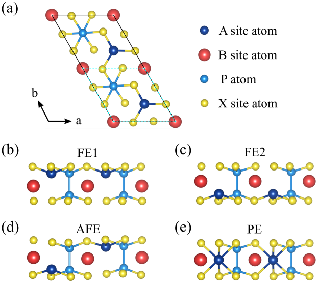
We begin by investigating the energetics of ABP2X6 monolayers obtained from first-principles calculations. We have considered PE, FE, and AFE orderings for all the systems, which are shown in Fig. 1. In the FE and AFE phases, the charge polarizations are out of plane mainly due to displacements of atoms. We use a supercell to model the AFE phase in which neighboring unit cells have opposite polarizations. The results are summarized in Table 1. One can see that for a number of ABP2X6 monolayers (A = Cu; B = In, Cr, V; and X = S, Se), the AFE phase has a lower energy than the PE and FE phases. For the FE phase, there are two energetically degenerate states, which are denoted as FE1 and FE2, respectively. In the presence of a substrate, the degeneracy is expected to be lifted. The trend of our results is in good agreement with previous studies Qi et al. (2018); Song et al. (2017); Hua et al. (2021); Lai et al. (2019); Sun et al. (2019); Huang et al. (2021); Feng et al. (2020).
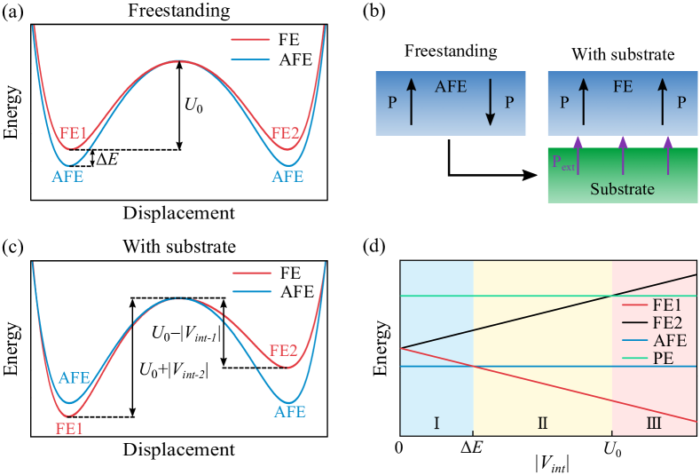
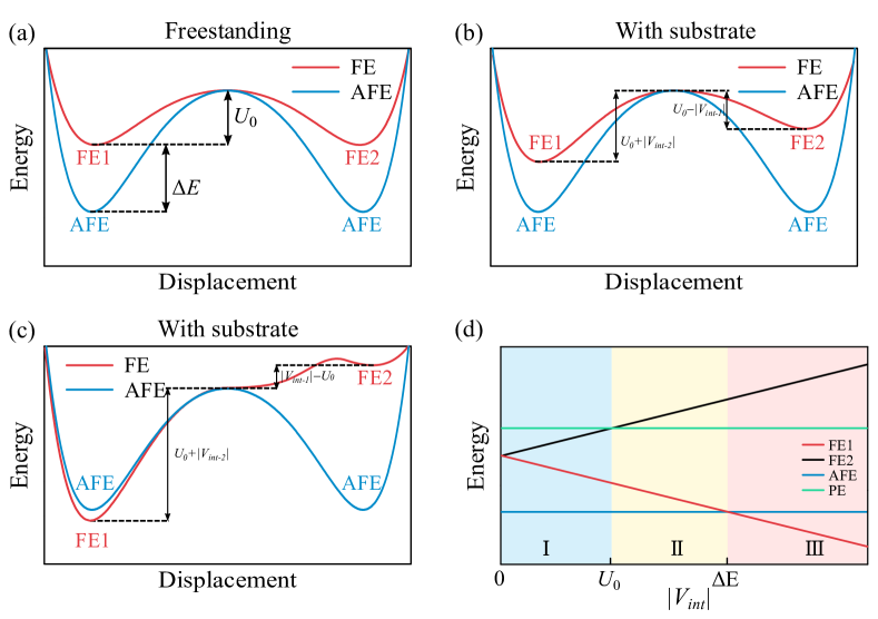
We now turn to our idea of interface engineering of ferroelectricity in ABP2X6 monolayers, which is shown in Fig. 2. The idea is pretty much similar to FE materials under external electric fields that the polarizations tend to be parallel to the fields. Instead, we make use of dipoles from substrates. The difference between using the electric fields and substrates is that the latter allows a nonvolatile tuning of the phase stability. Figure 2(a) schematically shows the potential energy of a free-standing ABP2X6 monolayer as a function of displacement of atoms. The FE and AFE phases are expected to have double-well-like potentials. For free-standing monolayers, the two FE phases are energetically degenerate. We focus on the systems for which the AFE phase is the ground state. Therefore, the AFE phase is assumed to have a lower energy than the FE phases. We denote the energy difference between the PE and FE phases as . Generally, is the energy barrier for the transform between the two FE phases. Likewise, denotes the energy difference between the FE and the AFE phases, i.e., . The potential energy per unit cell can be expanded into even terms of based on the Landau-Ginzburg formula. In the presence of external dipoles , there is an additional term that accounts for the coupling of and . This term, essentially a dipole-dipole interaction, has a form of , where is a constant and is the distance between and . We denote this term as . Then, the potential energy can be written as:
| (1) |
Therefore, the coupling lifts the degeneracy of the two FE phases: It lowers the total energy of one FE phase while it increases the total energy of the other one. The FE phase with parallel to is expected to have a lower energy than the one with antiparallel to . In contrast, the effects of this coupling on the total energies of the AFE and PE phases are expected to be negligible. As a result, the coupling changes the energy differences between the FE and the AFE phases and may thus enhance the stability of the FE phases [Figs. 2(b) and 2(c)]. In ABP2X6-based interfaces, two types of dipoles contribute to . One is ion-dipole () of the substrate such as the Mo-S dipoles in MoS2. The other one is the induced electronic polarization () in the substrate owing to the interface interaction.
We classify the AFE ABP2X6 monolayers listed in Table 1 into two categories according to comparisons of and : for type-I monolayers and for type-II systems, respectively. For type-I systems, the phase diagram of an AFE monolayer as a function of is shown in Fig. 2(d). In region I, the AFE phase remains to be the ground state since the strength of is smaller than . In region II, the coupling overcomes but remains smaller than , i.e., . In this case, FE1 has a lower energy than the AFE phase and FE2 remains to be a local minimum of the potential energy [see Fig. 2(c)]. Therefore, the two FE phases may be switched electrically. In region III, i.e., , FE1 remains to be the ground state, whereas FE2 is energetically higher than the PE phase. The coupling strengths for the two FE states are expected to be slightly different (the distance between and is slightly different). Therefore, in Fig. 2(c), we use and to denote the two couplings, respectively.
For type-II systems, the FE phases remain energetically higher than the AFE phase when enhancing the coupling strength such that can tune FE1 into the ground state. However, FE2 becomes energetically higher than the PE phase since (see Appendix B).
III.2 CuInP2Se6-based heterostructures
We now apply the above scheme to specific materials, which are CuInP2Se6 and CuCrP2S6 monolayers, respectively. Based on the values of and shown in Table. 1, both are type-I AFE systems. However, there is a significant difference between them. For the CuInP2Se6 monolayer, is small (less than 20 meV) and is much smaller than , whereas for the CuCrP2S6 monolayer, is relatively large and is comparable to . We choose different transition-metal dichalcogenide (TMD) monolayers, graphene, and h-BN monolayer as the substrates for the convenience of computation. Although a free-standing TMD monolayer is nonpolar, the local dipoles pointing from the top and bottom chalcogen atoms to the transition metal atoms are expected to have different effects on the total energy of the ABP2X6 monolayer. This is because these two types of dipoles have different distances to the dipole of the overlayer. The local dipoles next to the interface will dominate the coupling between the TMD and ABP2X6 monolayers.
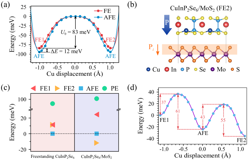
Figure 3(a) shows the potential energies of a free-standing CuInP2Se6 monolayer. The energy difference between the PE and the FE phases, i.e., , is about 83 meV. This value is much larger than the energy difference between the FE and the AFE phases, i.e., ( 12 meV). Such a small value of may be overcome by a vdW-type interfacial interaction between the overlayer and the substrate. We perform calculations of CuInP2Se6/MoS2 for a number of configurations. For each configuration, PE, FE1, FE2, and AFE phases are considered. We find that the two layers interact via a vdW-type bonding since there is a large layer distance between them ( 3.4 Å). FE2 has the lowest energy for each configuration. Figure 3(b) shows the side view of the lowest energy structure. The structures of other configurations are shown in Appendix C. From Fig. 3(c), one can see that the FE2 phase is about 12 meV lower than the AFE phase. Compared to the free-standing system, this result indicates that a vdW interface can lead to a change of about 24 meV in the total energy of a CuInP2Se6 monolayer. On the other hand, the FE1 phase is about 25 meV higher than the AFE phase but remains about 77 meV lower than the PE phase. We further investigate the kinetic pathway of FE phase transform for this structure using the climbing image nudged elastic band (CI-NEB) method Henkelman et al. (2000) for which the results are shown in Fig. 3(d). One can see that the FE2 phase remains to be a local minimum of the energy surface of CuInP2Se6/MoS2. Moreover, the barriers between different phases suggest that a nonvolatile switching of the FE phases is feasible.
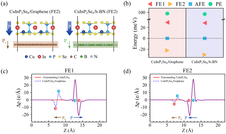
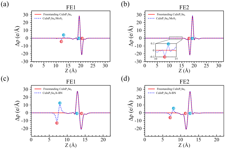
In addition to the MoS2 monolayer, we also investigate the effects of interfacing the CuInP2Se6 monolayer to graphene as well as a h-BN monolayer [Fig. 4(a)]. These substrates are distinct from the TMD monolayers in that they have no out-of-plane local dipoles next to the interface. Figure 4(b) shows that the energy of the FE2 ordering is about 20 (30) meV lower than the AFE phase when as the system is interfaced to graphene (a h-BN monolayer), whereas that of the FE1 phase is increased about 30 meV higher the AFE phase. The enhancements induced by these substrates are even slightly larger than that caused by a MoS2 monolayer. We further perform analyses over the charge-density difference between the FE and PE orderings, i.e., , from which the induced electronic polarization in the substrates can be obtained; and denote the charge densities of the FE and the PE orderings. One can see from Figs. 4(c) and 4(d) that is antiparallel and parallel with the polarization of the FE1 and FE2 orderings of the CuInP2Se6 monolayer, respectively. Therefore, the coupling between and lowers (increases) the energy of the FE2 (FE1) phase. We also perform similar analyses for CuInP2Se6/MoS2 and find that the electronic polarizations in the MoS2 monolayer induced by the CuInP2Se6 are negligibly small (see Appendix D). These results suggest that both the local dipoles of the substrates and the induced electronic polarizations in them are responsible for the enhancement of the FE ordering.
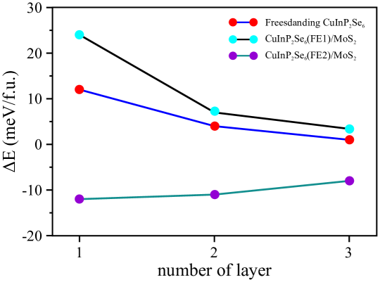
Song et al. reveal via first-principles calculations that CuInP2Se6 thin films with a size of less than six layers show AFE ordering within each layer (the layers are ferroelectrically coupled) Song et al. (2017). Films thicker than the critical size are found to be in the FE ordering. We perform calculations for its bilayer and trilayer supported by a MoS2 monolayer, for which the results are shown in Fig. 5. One can see that both are turned into FE in the heterostructures. One can expect that thicker multilayers can also be driven into the FE ordering as interfaced with MoS2, graphene, and h-BN monolayers.
III.3 CuCrP2S6-based heterostructures
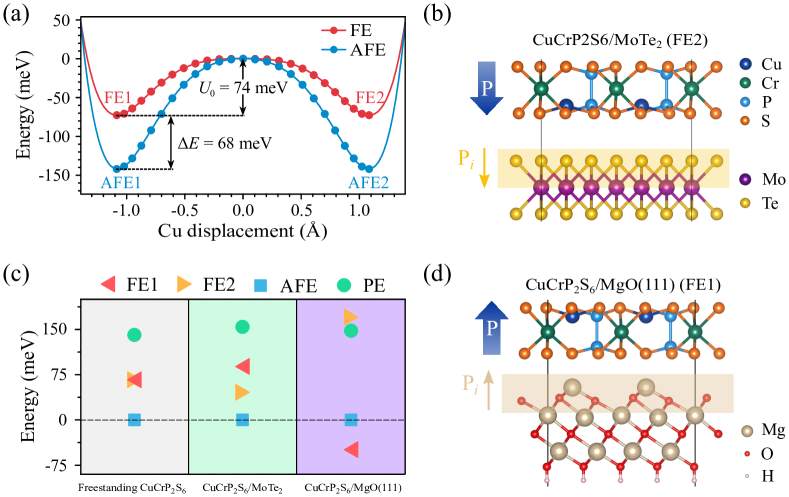
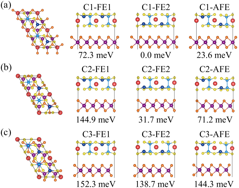
We now discuss the effects of interfacing on the phase stability of a CuCrP2S6 monolayer. The DFT+U method Dudarev et al. (1998) is used to treat electron correlations due to the partially filled -orbital of Cr for which a value of 3 eV is used Qi et al. (2018). From Fig. 6(a) as well as Table 1, one can see that for the free-standing CuCrP2S6 monolayer, the energy difference between the FE and the AFE phases, i.e., , is about 68 meV. This value is much larger than the energy change ( 25 meV) for a CuInP2Se6 monolayer induced by a MoS2 monolayer substrate. Geometric structures of the CuCrP2S6/MoTe2 heterostructures are shown in Fig. 6(b) and Appendix C. The layer distance between the two monolayers is about 3.3 Å, which implies that there is also a vdW-type interaction between them. Indeed, this interaction lowers the total energy of FE2 by about 20 meV. Specifically, the energy difference between it and the AFE phase decreases from 68 meV for the free-standing CuCrP2S6 monolayer to 46 meV for the supported one. However, the AFE phase remains to be the ground state [see the middle panel of Fig. 6(c)]. Therefore, vdW-type interfaces may not be effective in tuning FE properties of the CuCrP2S6 monolayer, although they do have a tendency to enhance the stability of the FE2 phase.
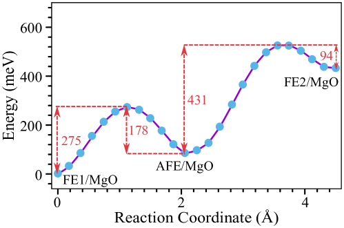
We further look at the effects of a polar substrate on the phase stability of the CuCrP2S6 monolayer. We choose MgO(111) as the substrate since it is a well-known polar surface. Previous studies revealed that this surface demonstrates various surface reconstructions, among which octopolar and p(1 2) reconstructions were already experimentally observed Finocchi et al. (2004); Zhang and Tang (2008). In our calculations, the p(1 2)-MgO(111) with Mg-termination is used as the substrate for the convenience of computation. The structures for the heterostructures are shown in Fig. 6(d) and Appendix D. Our calculations find that FE1 has a lower energy than the AFE phase by 50 meV. However, the total energy of FE2 is increased about 26 meV higher than the PE phase. Nonetheless, our NEB calculations shown in Appendix E suggest that there may still be a nonvolatile switching between the FE phases.
In addition, we perform calculations for the above CuInP2Se6- and CuCrP2S6-based interfaces using different vdW functionals/methods; the results are shown in Appendix F. One can see that these methods give the same trend in the stability of different orderings.
III.4 Polarization of interfaces
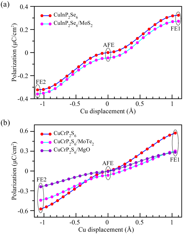
We now discuss the interfacing effects on the polarization of ABP2X6 monolayers. We calculate the polarization for each structure by artificially displacing the Cu atoms along the kinetic path FE1-AFE-FE2; the results are shown in Fig. 7. The results for the free-standing CuInP2Se6 and CuCrP2S6 monolayers are shown for comparison. For the FE1 state of CuInP2Se6/MoS2, the polarization is slightly smaller than that of the free-standing CuInP2Se6. By contrast, the polarization of the FE2 state is slightly enhanced as a result of interfacing. This behavior is because the induced electronic polarization is opposite to the polarization of the CuInP2Se6 monolayer for the FE1 state while parallel with for the FE2 state.
CuCrP2S6 shows different trend from CuInP2Se6 in that the polarizations for both states are reduced when it is interfaced with MoTe2 and MgO(111). For the FE1 state of CuCrP2S6/MoTe2, the reduction in the total polarization is because the whole system becomes metallic, which can be expected from the band alignments (see Appendix G). Thus, the screening effect reduces the polarization of the interface. For the FE2 state, the polarization reduction due to that the dipoles of the constituents are antiparallel with each other. For CuCrP2S6/MgO(111), the system is metallic in both the FE1 and FE2 phases due to strong interface bondings (see Appendix H). Therefore, a reduction in the total polarization can be naturally expected.
III.5 Band structure
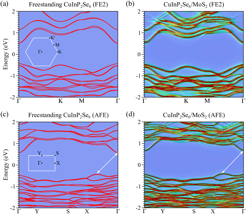
As already mentioned above for CuCrP2S6/MoTe2, the system experience a metal-insulator transition on a FE switch (see Fig. 16). The interfacing effect can also lead to tunable band structure for the CuInP2Se6 monolayers. Figure 8 shows that the FE phases of a CuInP2Se6 monolayer have a direct band gap of about 0.99 eV with both the valence band maximum (VBM) and conduction band minimum (CBM) located at . This band-gap size is comparable to that for Si, which is desired for optical applications. In contrast, the AFE phase is an indirect band-gap semiconductor with a gap size of about 1.03 eV. The CBM is located at , whereas the VBM is located at a point in between the and the X point. In the presence of a MoS2 monolayer, their bands remain almost unchanged. In particular, the nature of an indirect/direct band-gap is preserved, which is due to the vdW-type interaction between them. We further confirm that the nature of the band gap is maintained on small strains. We recall that for CuInP2Se6/MoS2 heterostructures, the FE2 phase becomes the ground state and the FE-AFE transition is ferroelectrically switchable. Therefore, this transition is accompanied by a switchable indirect-direct band-gap transition in the CuInP2Se6 monolayer, which makes the overlayer promising for optical and optoelectronic devices.
In conclusion, we have demonstrated that interface can be an effective way of engineering ferroelectricity in 2D ABP2X6 monolayers. In our model, the polarizations of the monolayers are coupled to local dipoles of the substrates and the induced electronic polarizations in the substrate. These couplings can stabilize the FE ordering, that is, they lower (increase) the total energy of one (the other) FE phase while keeping that of the AFE phase almost unchanged. We have applied the strategy to CuInP2Se6 and CuCrP2S6 monolayers, for which the energy difference () between the FE and the AFE phases are about 12 and 68 meV, respectively. The interfacial interaction between a CuInP2Se6 monolayer and vdW monolayers such as MoS2, graphene, and h-BN leads to an energy change of 25 30 meV for the FE phase and thus can overcome while keeping the other FE phase as a local minimum of the energy surface. Therefore, a FE switching is feasible for this system, which is supported by our NEB calculations. The vdW interfaces can also drive an AFE-to-FE phase transition for the multilayers of CuInP2Se6. However, in the case of a CuCrP2S6 monolayer, a vdW-type interface interaction is found to be insufficient to drive the FE-to-AFE phase transition. Interfacing it to a polar surface MgO(111) can make one of the FE orderings to be energetically lower than the AFE phase, for which a FE switching of different orderings is still likely. We further find a FE switching of electronic structure for CuInP2Se6 and CuCrP2S6-based interfaces. Our strategy is universal and can also be applied to other ABP2X6 monolayers and 2D materials with out-of-plane charge polarizations. Besides, our study can help understand the effects of interfacing in devices made of CuInP2S6 thin films and MoS2 substrate as already obtained by recent experiments Si et al. (2018); Wang et al. (2021).
Acknowledgements.
This work was supported by the National Natural Science Foundation of China (Grants No. 11774084, No. 12174098, No. U19A2090 and No. 91833302).IV APPENDIX
| Systems | FE | AFE | PE | Ground state |
| CuInP2S6 | 6.10 | 6.10 | 6.05 | AFE |
| CuInP2Se6 | 6.42 | 6.42 | 6.35 | AFE |
| CuBiP2S6 | 6.25 | 6.28 | 6.23 | FE |
| CuBiP2Se6 | 6.55 | 6.58 | 6.55 | FE |
| CuCrP2S6 | 6.02 | 6.02 | 6.00 | AFE |
| CuCrP2Se6 | 6.30 | 6.28 | 6.28 | AFE |
| CuVP2S6 | 5.98 | 5.98 | 5.93 | AFE |
| CuVP2Se6 | 6.30 | 6.30 | 6.28 | AFE |
| AgInP2S6 | N/A | N/A | 6.18 | PE |
| AgInP2Se6 | N/A | N/A | 6.48 | PE |
| AgBiP2S6 | 6.38 | 6.38 | 6.38 | FE |
| AgBiP2Se6 | 6.65 | 6.65 | 6.63 | FE |
IV.1 Lattice constants of different phases for ABP2X6
In Table 2, we show the optimized lattice constants of different phases for ABP2X6 monolayers. One can see that there are little differences in the lattice constant between different phases. Except for CuInP2S6, the ground states of the ABP2X6 monolayers from these calculations are consistent with those shown in Table 1 obtained from calculations using the lattice constant of the FE phase for AFE and PE phases.
IV.2 The phase diagram of type-II systems
Figure 9 schematically shows the phase diagram of type-II systems () under interactions between the ABP2X6 monolayers and substrates. The energy potentials of such a system shown in Fig. 9(a) for FE and AFE phases are similar to those for type-I systems [Fig. 2(a)]. The system remains AFE as long as [Fig. 9(b)]. Strong interactions that give can turn the system into FE. However, the other FE phase may have an energy higher than the AFE and PE phases [Fig. 9(c)]. The phase diagram shown in Fig. 9(d) is different from that of type-I systems in that the locations of and are interchanged.
IV.3 Geometric structures and energetics for ABP2X6/Substrates
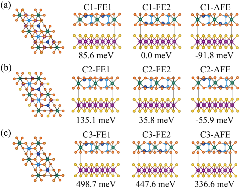
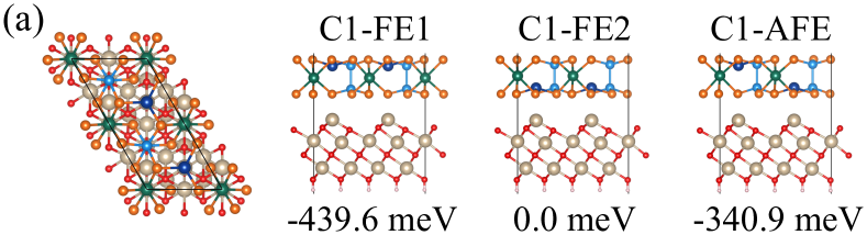
Figures. 1012 show the geometric structures of CuInP2Se6/MoS2, CuCrP2S6/MoTe2, and CuCrP2S6/MgO, respectively. The energy of each structure relative to that of the ground state structure is also given.
IV.4 Planar-averaged differential charge density
Figure 13 shows the planar-averaged charge density difference for CuInP2Se6/MoS2 and CuInP2Se6/h-BN. One can see that the induced electronic polarization in MoS2 is small for both FE orderings. By contrast, in h-BN is comparable to that for CuInP2Se6/graphene (see Fig. 4).
IV.5 Kinetic pathway of the FE phase transform for CuCrP2S6/MgO(111)
Figure 14 shows the kinetic pathway of FE phase transform for CuCrP2S6/MgO(111), which indicates that a FE switching of different orderings is feasible.
| Systems | vdW types | FE1 | FE2 | AFE | PE |
| CuInP2Se6 | * | 12 | 12 | 0 | 95 |
| CuInP2Se6/MoS2 | DFT-D2 | 24 | -12 | 0 | 101 |
| DFT-D3 | 29 | -63 | 0 | 60 | |
| optPBE | 14 | -23 | 0 | 115 | |
| CuCrP2S6 | * | 68 | 68 | 0 | 142 |
| CuCrP2S6/MoTe2 | DFT-D2 | 92 | 46 | 0 | 151 |
| DFT-D3 | 117 | 39 | 0 | 166 | |
| optPBE | 92 | 60 | 0 | 127 |
IV.6 Calculate with different vdWs functionals
The results shown in the main text were performed using DFT-D2 functional. In addition, we have carried out calculations using different vdWs functionals/methods for which the results are shown in Table 3. One can see that the results from different vdWs methods/functionals show essentially the same trend in the stability of different phases.
IV.7 Band alignments of CuInP2Se6 and CuCrP2S6 with the substrate
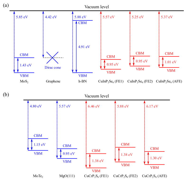
We investigate the workfunctions of the studied systems and their band alignments, for which the results are shown in Fig. 15. One can see that CuInP2Se6 and MoS2 as well as h-BN monolayers have a type-I or type-II band alignment for all the orderings. In addition, the Dirac point is located in the band gap of the FE2 and AFE phases of the CuInP2Se6 when their bands are aligned. So, charge transfers in CuInP2Se6/MoS2, CuInP2Se6/graphene, and CuInP2Se6/h-BN heterostructures are expected to be negligibly small.
By contrast, MoTe2 has a type-III band alignment with the FE1 phase of the CuCrP2S6 monolayer and has a type-II band alignment with the FE2 and AFE phases. This behavior helps to understand the band structures shown in Fig. 16. MgO(111) and the CuCrP2S6 monolayer has a type-II band alignment for all orderings. However, their heterostructures have a metallic band structure, which is due to the strong interfacial bonding.
IV.8 Band structures for CuCrP2S6/MoTe2 and CuCrP2S6/MgO(111)
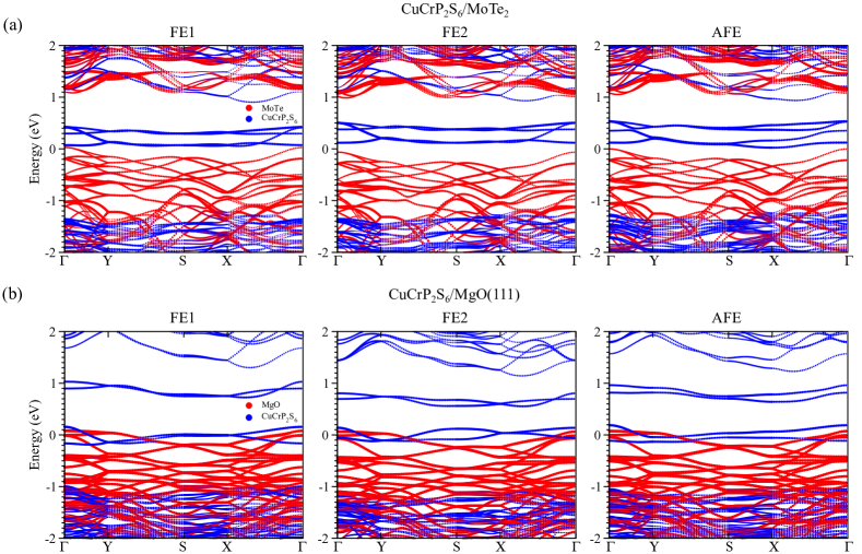
Figure 16 shows the band structures for CuCrP2S6/MoTe2 and CuCrP2S6/MgO(111). CuCrP2S6/MoTe2 remains semiconducting for the AFE and FE2 phases but becomes metallic for the FE1 phase. These behavior can be understood with the help of the band alignments shown in Fig. 15. For CuCrP2S6/MgO(111), all the band structures for the three orderings indicate that the heterostructure is metallic, which is due to the strong interfacing bonding between the overlayer and the substrate (the interlayer distance is about 2.3 Å).
References
- Junquera and Ghosez (2003) J. Junquera and P. Ghosez, Nature 422, 506–509 (2003).
- Zhong et al. (1994) W. Zhong, R. D. King-Smith, and D. Vanderbilt, Phys. Rev. Lett. 72, 3618 (1994).
- Fong et al. (2004) D. D. Fong, G. B. Stephenson, S. K. Streiffer, J. A. Eastman, O. Auciello, P. H. Fuoss, and C. Thompson, Science 304, 1650 (2004).
- Stengel et al. (2010) M. Stengel, N. A. Spaldin, and D. Vanderbilt, Nat. Phys. 5, 304 (2010).
- Almahmoud et al. (2010) E. Almahmoud, I. Kornev, and L. Bellaiche, Phys. Rev. B 81, 064105 (2010).
- Chang et al. (2016) K. Chang, J. Liu, H. Lin, N. Wang, K. Zhao, A. Zhang, F. Jin, Y. Zhong, X. Hu, W. Duan, Q. Zhang, L. Fu, Q.-K. Xue, X. Chen, and S.-H. Ji, Science 353, 274 (2016).
- Fei et al. (2016) R. Fei, W. Kang, and L. Yang, Phys. Rev. Lett. 117, 097601 (2016).
- Higashitarumizu et al. (2020) N. Higashitarumizu, H. Kawamoto, C.-J. Lee, B.-H. Lin, F.-H. Chu, I. Yonemori, T. Nishimura, K. Wakabayashi, W.-H. Chang, and K. Nagashio, Nat. Commun. 11, 2428 (2020).
- Ding et al. (2017) W. Ding, J. Zhu, Z. Wang, Y. Gao, D. Xiao, Y. Gu, Z. Zhang, and W. Zhu, Nat. Commun. 8, 14956 (2017).
- Zhou et al. (2017) Y. Zhou, D. Wu, Y. Zhu, Y. Cho, Q. He, X. Yang, K. Herrera, Z. Chu, Y. Han, M. C. Downer, H. Peng, and K. Lai, Nano Lett. 17, 5508 (2017).
- Cui et al. (2018) C. Cui, W.-J. Hu, X. Yan, C. Addiego, W. Gao, Y. Wang, Z. Wang, L. Li, Y. Cheng, P. Li, X. Zhang, H. N. Alshareef, T. Wu, W. Zhu, X. Pan, and L.-J. Li, Nano Lett. 18, 1253 (2018).
- Liu et al. (2016) F. Liu, L. You, K. L. Seyler, X. Li, P. Yu, J. Lin, X. Wang, J. Zhou, H. Wang, H. He, S. T. Pantelides, W. Zhou, P. Sharma, X. Xu, P. M. Ajayan, J. Wang, and Z. Liu, Nat. Commun. 7, 12357 (2016).
- Belianinov et al. (2015) A. Belianinov, Q. He, A. Dziaugys, P. Maksymovych, E. Eliseev, A. Borisevich, A. Morozovska, J. Banys, Y. Vysochanskii, and S. V. Kalinin, Nano Lett. 15, 3808 (2015).
- Wan et al. (2017) W. Wan, C. Liu, W. Xiao, and Y. Yao, Appl. Phys. Lett. 111, 132904 (2017).
- Xu et al. (2017) B. Xu, H. Xiang, Y. Xia, K. Jiang, X. Wan, J. He, J. Yin, and Z. Liu, Nanoscale 9, 8427 (2017).
- Xiao et al. (2018) C. Xiao, F. Wang, S. A. Yang, Y. Lu, Y. Feng, and S. Zhang, Adv. Funct. Mater. 28, 1707383 (2018).
- Lin et al. (2019) L.-F. Lin, Y. Zhang, A. Moreo, E. Dagotto, and S. Dong, Phys. Rev. Lett. 123, 067601 (2019).
- Zhong et al. (2019) T. Zhong, X. Li, M. Wu, and J.-M. Liu, Natl. Sci. Rev. 7, 373 (2019).
- Xu et al. (2020a) C. Xu, P. Chen, H. Tan, Y. Yang, H. Xiang, and L. Bellaiche, Phys. Rev. Lett. 125, 037203 (2020a).
- Xu et al. (2020b) M. Xu, C. Huang, Y. Li, S. Liu, X. Zhong, P. Jena, E. Kan, and Y. Wang, Phys. Rev. Lett. 124, 067602 (2020b).
- Ma et al. (2021) X.-Y. Ma, H.-Y. Lyu, K.-R. Hao, Y.-M. Zhao, X. Qian, Q.-B. Yan, and G. Su, Sci. Bull. 66, 233 (2021).
- Hua et al. (2021) C. Hua, H. Bai, Y. Zheng, Z.-A. Xu, S. A. Yang, Y. Lu, and S.-H. Wei, Chin. Phys. Lett. 38, 077501 (2021).
- Bai et al. (2020) H. Bai, X. Wang, W. Wu, P. He, Z. Xu, S. A. Yang, and Y. Lu, Phys. Rev. B 102, 235403 (2020).
- Qi et al. (2018) J. Qi, H. Wang, X. Chen, and X. Qian, Appl. Phys. Lett. 113, 043102 (2018).
- Lai et al. (2019) Y. Lai, Z. Song, Y. Wan, M. Xue, C. Wang, Y. Ye, L. Dai, Z. Zhang, W. Yang, H. Du, and J. Yang, Nanoscale 11, 5163 (2019).
- Song et al. (2017) W. Song, R. Fei, and L. Yang, Phys. Rev. B 96, 235420 (2017).
- Sun et al. (2019) Z.-Z. Sun, W. Xun, L. Jiang, J.-L. Zhong, and Y.-Z. Wu, J. Phys. D: Appl. Phys. 52, 465302 (2019).
- Feng et al. (2020) X. Feng, J. Liu, X. Ma, and M. Zhao, Phys. Chem. Chem. Phys. 22, 7489 (2020).
- Huang et al. (2021) S. Huang, Z. Shuai, and D. Wang, J. Mater. Chem. A 9, 2734 (2021).
- Dziaugys et al. (2020) A. Dziaugys, K. Kelley, J. A. Brehm, L. Tao, A. Puretzky, T. Feng, A. O’Hara, S. Neumayer, M. Chyasnavichyus, E. A. Eliseev, J. Banys, Y. Vysochanskii, F. Ye, B. C. Chakoumakos, M. A. Susner, M. A. McGuire, S. V. Kalinin, P. Ganesh, N. Balke, S. T. Pantelides, A. N. Morozovska, and P. Maksymovych, Nat. Commun. 11, 3623 (2020).
- Kresse and Furthmüller (1996) G. Kresse and J. Furthmüller, Phys. Rev. B 54, 11169 (1996).
- Blöchl (1994) P. E. Blöchl, Phys. Rev. B 50, 17953 (1994).
- Kresse and Joubert (1999) G. Kresse and D. Joubert, Phys. Rev. B 59, 1758 (1999).
- Bučko et al. (2010) T. Bučko, J. Hafner, S. Lebègue, and J. G. Ángyán, J. Phys. Chem. A 114, 11814 (2010).
- Klimeš et al. (2009) J. Klimeš, D. R. Bowler, and A. Michaelides, J. Phys.: Condens. Matter 22, 022201 (2009).
- Klimeš et al. (2011) J. c. v. Klimeš, D. R. Bowler, and A. Michaelides, Phys. Rev. B 83, 195131 (2011).
- Chen and Weinert (2014) M. X. Chen and M. Weinert, Nano Lett. 14, 5189 (2014).
- Chen et al. (2017) M. X. Chen, W. Chen, Z. Zhang, and M. Weinert, Phys. Rev. B 96, 245111 (2017).
- Chen and Weinert (2018) M. Chen and M. Weinert, Phys. Rev. B 98, 245421 (2018).
- Henkelman et al. (2000) G. Henkelman, B. P. Uberuaga, and H. Jónsson, J. Chem. Phys. 113, 9901 (2000).
- Dudarev et al. (1998) S. L. Dudarev, G. A. Botton, S. Y. Savrasov, C. J. Humphreys, and A. P. Sutton, Phys. Rev. B 57, 1505 (1998).
- Finocchi et al. (2004) F. Finocchi, A. Barbier, J. Jupille, and C. Noguera, Phys. Rev. Lett. 92, 136101 (2004).
- Zhang and Tang (2008) W.-B. Zhang and B.-Y. Tang, J. Phys. Chem. C 112, 3327 (2008).
- Si et al. (2018) M. Si, P.-Y. Liao, G. Qiu, Y. Duan, and P. D. Ye, ACS Nano 12, 6700 (2018).
- Wang et al. (2021) X. Wang, C. Zhu, Y. Deng, R. Duan, J. Chen, Q. Zeng, J. Zhou, Q. Fu, L. You, S. Liu, J. H. Edgar, P. Yu, and Z. Liu, Nat. Commun. 12, 1109 (2021).