A study of singlet fission-halide perovskite interfaces
Abstract
A method for improving the efficiency of solar cells is combining a low-bandgap semiconductor with a singlet fission material (which converts one high energy singlet into two low energy triplets following photoexcitation). Here we present a study of the interface between singlet fission molecules and low-bandgap halide pervoskites. We briefly show a range of experiments screening for triplet transfer into a halide perovskite. However, in all cases triplet transfer was not observed. This motivated us to understand the halide perovskite/singlet fission interface better by carrying out first-principles calculations using tetracene and cesium lead iodide. We found that tetracene molecules/thin films preferentially orient themselves parallel to/perpendicular to the halide perovskite’s surface, in a similar way to on other inorganic semiconductors. We present formation energies of all interfaces, which are significantly less favourable than for bulk tetracene, indicative of weak interaction at the interface. It was not possible to calculate excitonic states at the full interface due to computational limitations, so we instead present highly speculative toy interfaces between tetracene and a halide-perovskite-like structure. In these models we focus on replicating tetracene’s electronic states correctly. We find that tetracene’s singlet and triplet energies are comparable to that of bulk tetracene, and the triplet is strongly localised on a single tetracene molecule, even at an interface. Our work provides new understanding of the interface between tetracene and halide perovskites, explores the potential for modelling excitons at interfaces, and begins to explain the difficulties in extracting triplets directly into inorganic semiconductors.
I Introduction
Material surfaces and interfaces are important in a range of technologies and govern processes including sample growth, ion mixing, charge transfer, and electronic passivationYadav et al. (2017); Martha et al. (2009); Yang, Dou, and Wang (2018); Andaji-Garmaroudi et al. (2020); Stadlober et al. (2006); DeQuilettes et al. (2016); Zhang et al. (2015). An interface of particular interest for the next generation of solar cells is that between a singlet fission material and an inorganic semiconductor. Singlet fission materials have the unusual property that when a singlet is generated (following photoexcitation) it is rapidly converted into two triplets Smith and Michl (2010). If combined with an inorganic semiconductor harvesting low energy wavelengths of the solar spectrum, such a solar cell could surpass the Shockley-Queisser single junction efficiency limit of 33 % Tayebjee, McCamey, and Schmidt (2015). Key to this technology working is the ability to extract at least part of the triplet excitons from the singlet fission material. Ideally triplets would be transferred directly into, or separated at, an interface with an inorganic semiconductor (exciton transfer and exciton dissociation). Triplet excitons cannot undergo Förster energy transfer Scholes (2003), as they do not have a dipole moment (unlike singlet excitons). Therefore, charge transfer must proceed via Dexter processes, which are far shorter-ranged in nature and governed by wavefunction overlap Dexter (1953).
In studies of clean silicon surfaces with singlet fission materials deposited on them, the component of triplet transfer has been negligible Piland et al. (2014); Macqueen et al. (2018). However, extraction of triplets has been achieved into PbS and PbSe quantum dots, as well as more recently silicon Tabachnyk et al. (2014); Thompson et al. (2014); Einzinger et al. (2019). In these cases there has been some modification of the inorganic semiconductor’s surface or a direct chemical bond from it to the singlet fission material. More generally it has proven difficult to extract triplets directly from singlet fission materials into inorganic semiconductors, and a full understanding of the difficulties involved is lacking.
Here, we explore the interface between singlet fission materials and halide perovskites. First, we briefly present experiments screening for triplet transfer from singlet fission materials to low-bandgap (< eV) halide perovskites. Despite modified fission activity in the organic, in all cases we observed singlet transfer or no transfer to the halide perovskite. These experiments motivated us to understand the interface better via a first principles computational study. We modelled the interface between the singlet fission material tetracene and caesium lead iodide (CsPbI3, noting that in our computations the bulk halide perovskite has a bandgap lower than tetracene’s triplet energy) Green, Ho-Baillie, and Snaith (2014). We find that the tetracene/CsPbI3 interface is not very energetically favourable to form and films of tetracene form with the long axis of the molecule perpendicular to the halide perovskite surface. We also present highly speculative calculations suggesting that triplets remain strongly localised on tetracene, even at the interface. Our computational results go some way to explaining experimental observations and suggest a clear route forward for future studies.
II Brief experimental screening
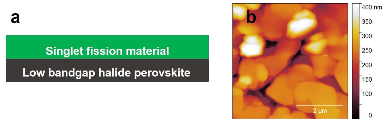
We fabricated approximately 150 samples as low-bandgap (< eV) halide perovskites/singlet fission bilayers (see schematic, supplementary information Figure 6a). A full list of all processing routes explored can be found in SI A.
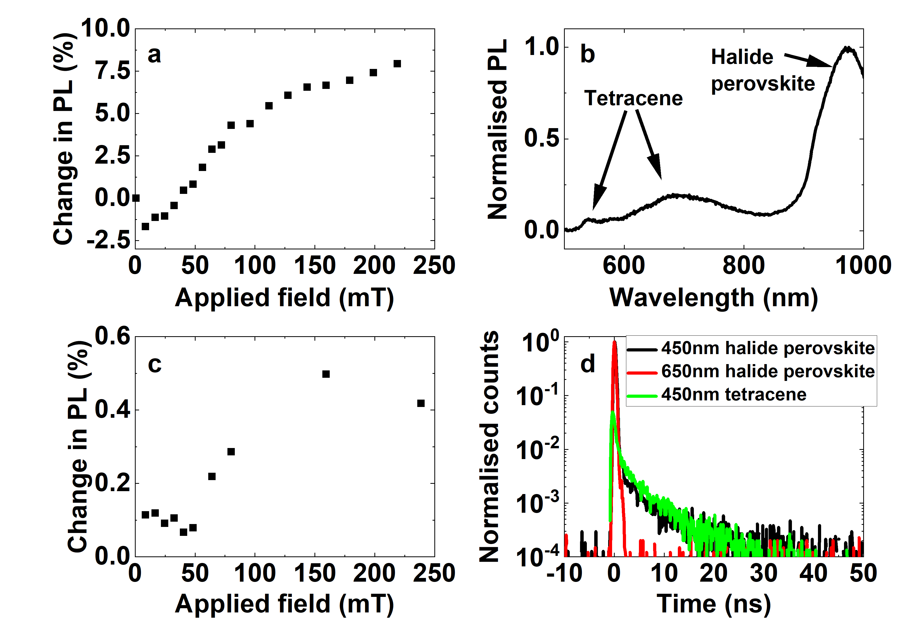
We probed triplet transfer by applying a magnetic field to the singlet fission/halide perovskite bilayer and observing the change in the halide perovskite’s photoluminescence (PL) and via time correlated single photon counting (TCSPC). If there is net triplet transfer or dissociation at the interface the halide perovskite’s PL will reduce at high magnetic field as it will receive fewer triplets Merrifield (1968).
Two singlet fission materials were used in our screening experiments: tetracene and 1,6-Diphenyl-1,3,5-hexatriene (DPH) Merrifield, Avakian, and Groff (1969); Wilson et al. (2013); Dillon, Piland, and Bardeen (2013); Wakasa et al. (2015). The triplet energies in these molecules ( eV and eV respectively) are larger than the selected halide perovskite’s bandgap ( eV) and they both have high triplet yields (with > % of singlets converted to triplets).
When we began this study, it had recently been observed that adding small quantities of transition metals into halide perovskites could change their work function Klug et al. (2017). A similar effect could be seen by changing the quantity of caesium at the A site of the halide perovskite Prasanna et al. (2017). In both cases the halide perovskite’s bandgap remains constant. Halide perovskites with different work functions were fabricated according to these two methods. All samples had either 50:50 or 25:75 ratios of lead to tin, corresponding to bandgaps in the - eV range. We fabricated films that were thin ( - nm) to increase any singlet fission contribution to the halide perovskite’s photoluminescence.
We present an example of the results obtained from these screening experiments in supplementary Figure 7, for a tetracene/FA0.9Cs0.1Pb0.25Sn0.75I3 bilayer (with tetracene evaporated on to the halide perovskite, where FA is formamidinium). We present the magnetic PL response of evaporated tetracene in Figure 7a, showing an increase in PL at high magnetic field, as expected. In Figure 7b the photoluminescence of the bilayer is presented (from nm to nm). Tetracene can be weakly observed in the nm to nm region (it is weak due to the camera used, see figure caption), and the halide perovskite PL peaks at nm. We were able to selectively monitor the halide perovskite’s PL change with magnetic field by using a nm long-pass filter, as shown in Figure 7c. At low magnetic field the change in PL is < %, which is within the experimental noise. However, at high magnetic field the halide perovskite’s PL increases to a significant level (> %), indicating net singlet transfer from tetracene. Singlet transfer is confirmed by TCSPC, as shown in Figure 7d. By exciting the bilayer above and below tetracene’s bandgap and observing the halide perovskite’s time resolved photoluminescence (TRPL), we observe the longer lived component of this TRPL coincides well with the TRPL from tetracene (in the bilayer). Furthermore, we find the halide perovskite’s TRPL shows nothing longer lived than the singlet transfer, suggesting any triplet transfer from tetracene is negligible (noting triplets are typically longer lived than singlets).
In all cases explored, we observed singlet fission in the organic layer but no net triplet transfer to the halide perovskite (though singlet transfer was readily observed). To better understand organic/inorganic interfaces, and potentially explore the reasons for the lack of triplet transfer from singlet fission materials, we modelled a proto-typical singlet fission/halide perovskite bilayer.
III Modelling background
It has recently become possible to study some simple interfaces with first-principles computational methods. For example, density functional theory (DFT) calculations (corroborated by X-ray diffraction experiments) have helped confirm the geometry of the interface between tetracene and silicon Janke et al. (2020); Niederhausen et al. (2020), where tetracene thin films were found to orient with their long axis perpendicular to the semiconductor surface.
Here, we model tetracene and CsPbI3 using DFT. We selected CsPbI3 for this study as the cation has spherical symmetry (unlike methylammonium or formamidinium) and an inorganic lead halide perovskite reduces the number of atomic species in the system, simplifying modelling while maintaining the same basic electronic structure. We note that the electronic structure of halide perovskites is governed by the metal/halide framework, so as long as this is maintained we anticipate results will be comparable for different compositions. As the literature has shown that it has been difficult to obtain triplet transfer to several different semiconductors, we postulate that the reason for lack of triplet transfer lies primarily within the singlet fission material. This is further supported by halide perovskites sensitising triplet states in singlet fission materials Lu et al. (2019). Therefore, our modelling focuses on correctly reproducing tetracene’s electronic states (at the expense of correctly modelling the halide perovskite’s electronic states).
We first discuss each system in isolation and quantify the effects of surface terminations and bandgap corrections. We then present geometry arrangements and resulting electronic structures of a single tetracene molecule and bulk tetracene films on a halide perovskite surface. As in previous studies Janke et al. (2020), we found post-DFT and BSE calculations (required to calculate excitonic states) of full interfaces were not feasible. Instead, we present highly speculative toy models between tetracene and a halide perovskite-like structure. We focus on correctly reproducing tetracene’s electronic states at the interface (at the expense of the halide perovskite). All computational details for subsequent sections can be found in supplementary information C.
IV Tetracene
Tetracene is one of the most widely studied singlet fission materialsMerrifield, Avakian, and Groff (1969); Avakian and Merrifield (1968); Smith and Michl (2010); Tayebjee, Clady, and Schmidt (2013); Stern et al. (2017). It undergoes singlet fission endothermically and, consequently, the process proceeds at a slower pace than in other moleculesWilson et al. (2013). Amongst singlet fission materials, its triplet energy is one of the highest, making it one of the most relevant for solar energy applicationsWu et al. (2014). Initially, we carried out geometry relaxations of bulk tetracene unit cells using several different exchange correlation functionals and Van der Waals corrections. We found the PBE generalised gradient approximation, coupled to a Tkatchenko-Scheffler (TS) Van der Waals semi-empirical correction, best reproduce experimental tetracene lattice parameters, in agreement with other analyses Tkatchenko and Scheffler (2009); Janke et al. (2020) (see supplementary information Table 3). We used this functional and Van der Waals correction in all subsequent calculations.
In Figure 1a we plot the DFT-level bandgap for different relaxed tetracene surfaces versus the number of tetracene repeating units in the non-periodic direction. Modelled surfaces are termed ‘cut 1’ and ‘cut 2’ (other cuts were not commensurate with the halide perovskite unit cell), as shown on the inset. While cut 1 has relatively little effect on the DFT-level bandgap, cut 2 results in a bandgap increase of eV for a single repeating unit, which reduces to within eV by three repeating units. This demonstrates there is relatively little electronic interaction between tetracene layers (i.e. in the direction perpendicular to cut 1); rather, electronic states are mostly localised to one layer.
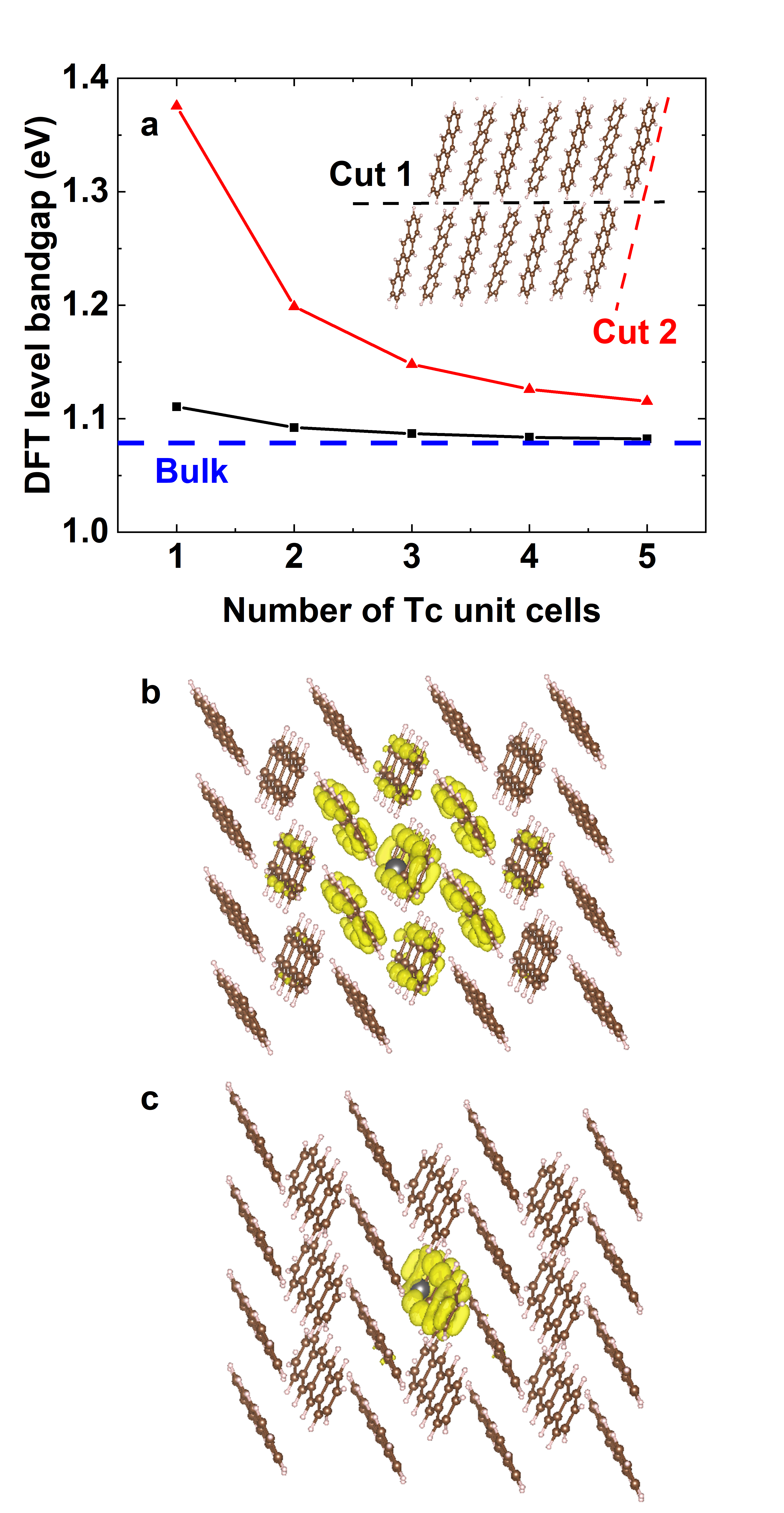
Tetracene’s (optically) excited states typically exist as singlets and triplets. We used a one-shot calculation together with the Bethe-Salpeter equation to calculate the singlet and triplet states of bulk tetracene. The lowest energy singlet and triplet states of relaxed tetracene have energies of 2.08 eV and 1.24 eV respectively, which increase to 2.22 eV and 1.27 eV when using experimental lattice parameters, in good agreement with experimental results Tomkiewicz, Groff, and Avakian (1971); Wilson et al. (2013). While it is not possible to plot excitonic wavefunctions (as these are two-particle states requiring six spatial coordinates), it is possible to plot electron or hole charge densities with the other particle fixed in place. In Figure 1b and c we plot the electronic charge density for the lowest energy singlet and triplet states respectively, with the hole fixed at a carbon atom (grey sphere). The singlet state is delocalised over several molecules but the triplet is almost fully localised to a single molecule, as has been previously discussed by others Alvertis et al. (2020). We found this to be the case for the hole being fixed at several different positions within the tetracene film. Furthermore, neither the singlet nor triplet states have significant wavefunction overlap between planes of the film (in direction perpendicular to cut 1), again showing that films have quasi-two-dimensional electronic states.
V Caesium lead iodide
We discuss the electronic structure of bulk CsPbI3 in supplementary information E. When we consider an interface there are many possible surface terminations for a cubic inorganic structure. First-principles calculations on related halide perovskites suggest (100) surfaces are the most likely to form so our study focsues on these surfaces Haruyama et al. (2014). We consider two possible surface terminations of this plane: PbI2 and CsI. In all our modelling the same surface was used on both sides of the halide perovskite, mitigating surface dipole effects. We present the valence band charge densities for these two relaxed surface terminations in Figure 2a and b. While the CsI termination has the valence band confined to the bulk, PbI2 termination has a significant surface contribution (i.e. a dangling bond). This gives two significantly different situations, so our subsequent calculations explore both surfaces. We note that PbI2 surfaces are lower in energy so are more likely to form in reality. In both materials the conduction band is confined to the bulk.
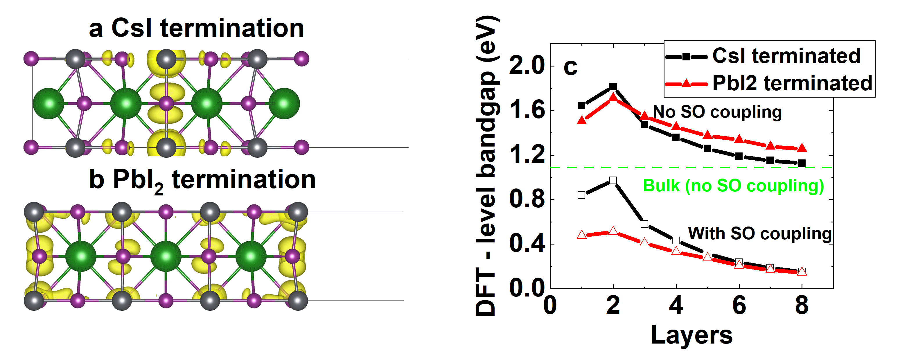
The electronic structure of halide perovskites is fundamentally three-dimensional, so it is strongly affected by quantum confinement. In Figure 2c we present the DFT-level bandgap of CsPbI3 for both relaxed surface terminations, as a function of the number of repeating units in the vacuum direction, both with and without spin-orbit coupling. In all cases a significant increase in bandgaps is found when compared to the bulk, as expected. We find CsI terminated surfaces have slightly larger bandgaps, which is attributed to more confined states (c.f. Figure 2a and b).
VI Tetracene molecules on halide perovskite surfaces
To simulate a halide perovskite thin film, we modelled three halide perovskite layers in the non-periodic direction, as inter-atomic distances in the centre of this structure were comparable to distances in bulk CsPbI3 (see supplementary information Table 4) and computation was not too expensive. As has been discussed elsewhere Niederhausen et al. (2020); Hlawacek and Teichert (2013); Janke et al. (2020), there are three main orientations for a tetracene molecule to lie on a halide perovskite surface: with the long axis of the molecule perpendicular; the short axis of the molecule perpendicular; or face-on to the halide perovskite (termed parallel, see Figure 3a).
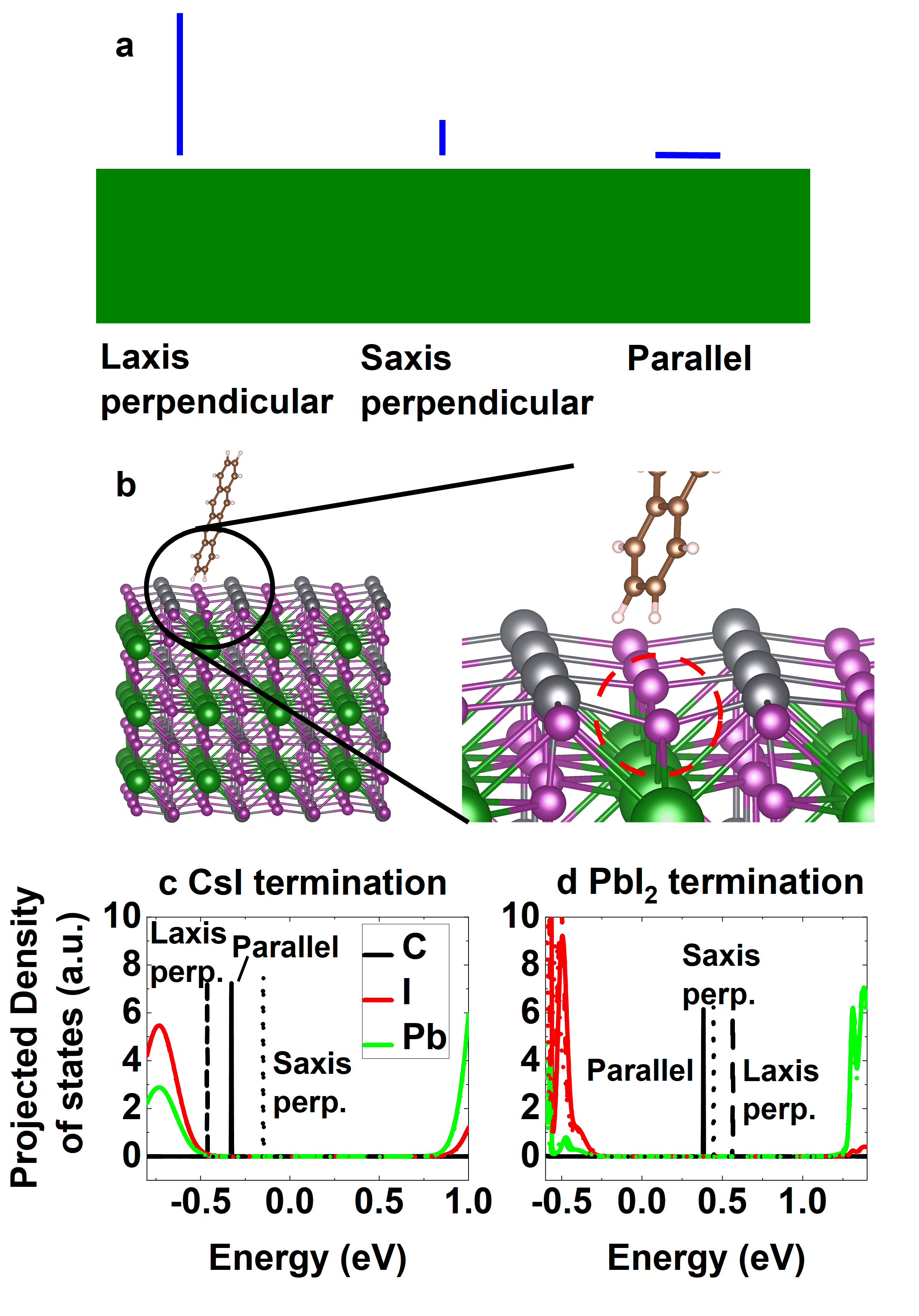
We carried out geometry relaxations for the three tetracene orientations on both halide perovskite surfaces (i.e. six simulations). The relaxed energy is relatively independent of where the tetracene is initially placed above a semiconductor Janke et al. (2020), so we only considered one starting position for each geometry relaxation. We present an example of a relaxed geometry in Figure 3b. The tetracene molecule is observed to remain unchanged, while the halide perovskite surface distorts. We found qualitatively similar results in all simulations. This is reasonable as halide perovskites have surprisingly low Young’s moduli for inorganic semiconductors, comparable to those of relevant organic crystals Sun et al. (2015); Jhou et al. (2019); Wortman and Evans (1965); Chen et al. (2016).
The formation energy between the halide perovskite surface and the tetracene molecule is given by Eformation=Einterface-(Eperov,slab+Etetracene,molecule), that is the energy of the interface less the energy of the halide perovskite slab and tetracene molecule in vacuum. We present Eformation for the six geometries considered in Table 1. Results suggest the parallel tetracene arrangement has the most favourable formation energy. This is in agreement with other examples of rod-like molecules on the surface of inorganic semiconductors Janke et al. (2020); Niederhausen et al. (2020); Hlawacek and Teichert (2013). Furthermore, in all cases we find the interaction energy is observed to be weak: for comparison the formation energy for a tetracene film is eV per molecule.
| Tetracene orientation | (eV) |
|---|---|
| CsI termination | |
| Long axis perpendicular | |
| Short axis perpendicular | |
| Parallel | |
| PbI2 termination | |
| Long axis perpendicular | |
| Short axis perpendicular | |
| Parallel |
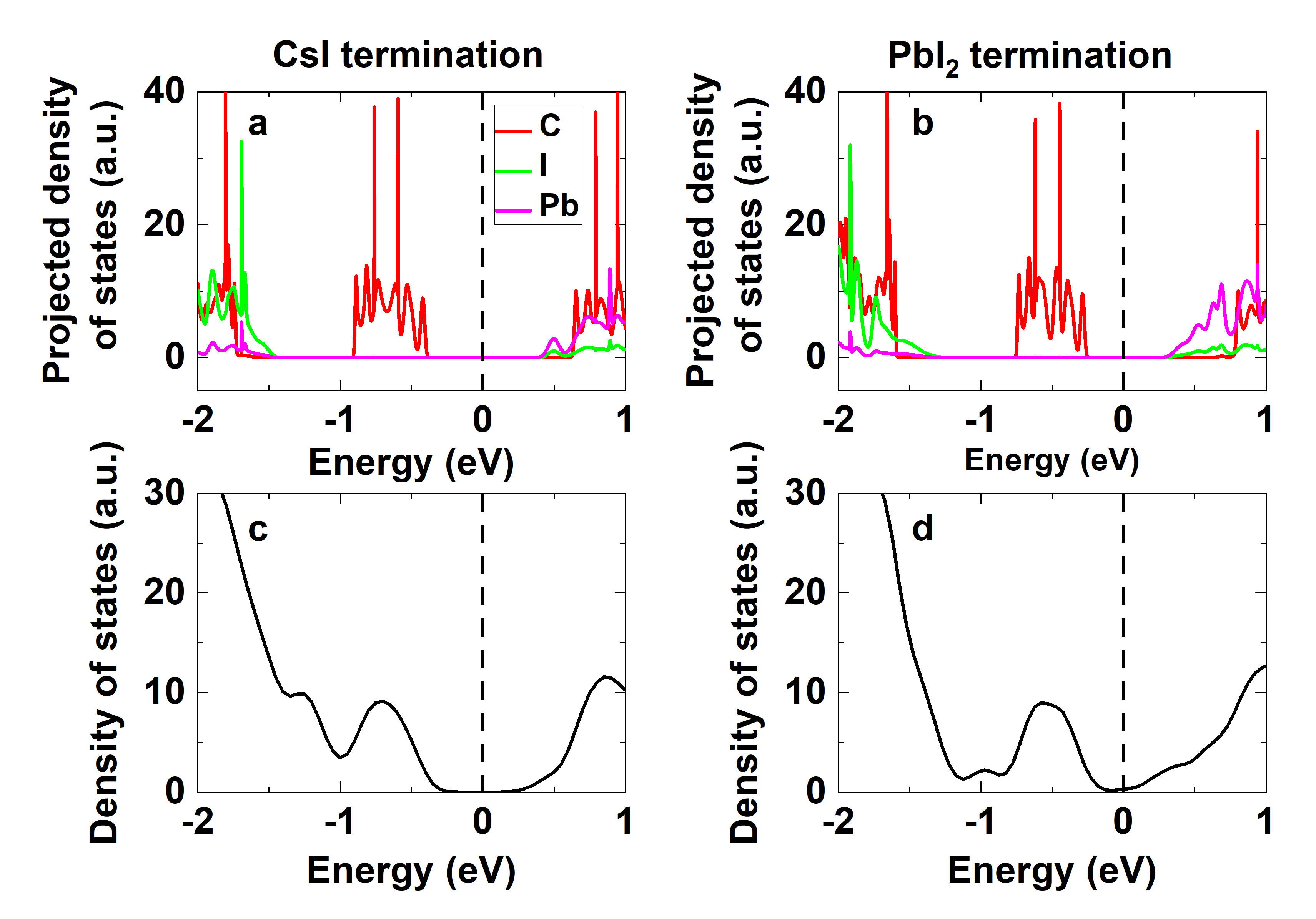
In order to understand band-alignment at each interface, we calculated the projected density of states (PDOS), with projection onto each species’ atomic orbitals. We neglected spin-orbit coupling as this gives a similar halide perovskite bandgap to that obtained with spin-orbit coupling and a correction at significantly less computational cost (see supplementary information section V). Our results are presented in Figure 3c and d. For CsI terminated surfaces, as the halide perovskite’s valence band is localised in the bulk of the structure (c.f. Figure 2a), its PDOS is unchanged for different tetracene orientations (Figure 3c). For the (energetically favoured) parallel and short-axis perpendicular orientations, tetracene’s valence band lies above that of the halide perovskite while for the long-axis perpendicular model its valence band aligns with the halide perovskite’s valence band maximum. For PbI2 termination, as the halide perovskite’s valence band has some surface character, we find there is a small variation in the halide perovskite’s PDOS for the different simulations (Figure 3d). Importantly, tetracene’s valence band is above the halide perovskite’s in all cases, and significantly more offset from the halide perovskite’s valence band than in the CsI terminated case. We attribute this to PbI2 terminated surfaces being lower in energy than CsI terminated surfaces rather than a significant change in tetracene’s electronic structure. Tetracene’s valence band being above the halide perovskite’s is indicative of tetracene being a good hole extracting material, as has been observed experimentally in halide perovskite/tetracene interfaces Abdi-Jalebi et al. (2019).
VII Tetracene-halide perovskite thin film interface
To model interfaces between bulk materials, unit cells with commensurate in-plane lattice parameters need to be found. We identified two tetracene/halide perovskite interfaces with tetracene’s ‘cut 1’ surface termination and one with ‘cut 2’ surface termination. They are shown in supplementary information Figure 9. We were not able to find any commensurate unit cells of reasonable size for tetracene’s third possible exposed plane. These three simulations are termed ‘cut 1 no rotation’, ‘cut 1 with rotation’ and ‘cut 2’. The two cut 1 simulations have normal strains of < 3 % and shear strain of %, while cut 2 has both normal and shear strains on the order of % (see supplementary information Table 5 for all strains). Two tetracene unit cells were used in the non-periodic direction for cut 1 models, and four tetracene units cells for cut 2 (based on results shown in Figure 1a). This resulted in large cells for DFT simulations so no vacuum layer was used i.e. there were two interfaces between tetracene and the halide perovskite. This also reduced the possibility of any dipole effects. The distance between adjacent halide perovskite and adjacent tetracene layers was at least as large as the vacuum spacing required to prevent interaction between adjacent layers of the same material in the non-periodic direction. As tetracene and halide perovskites have comparable Young’s moduli, we allowed lattice parameters to vary in geometry relaxations Sun et al. (2015); Jhou et al. (2019).
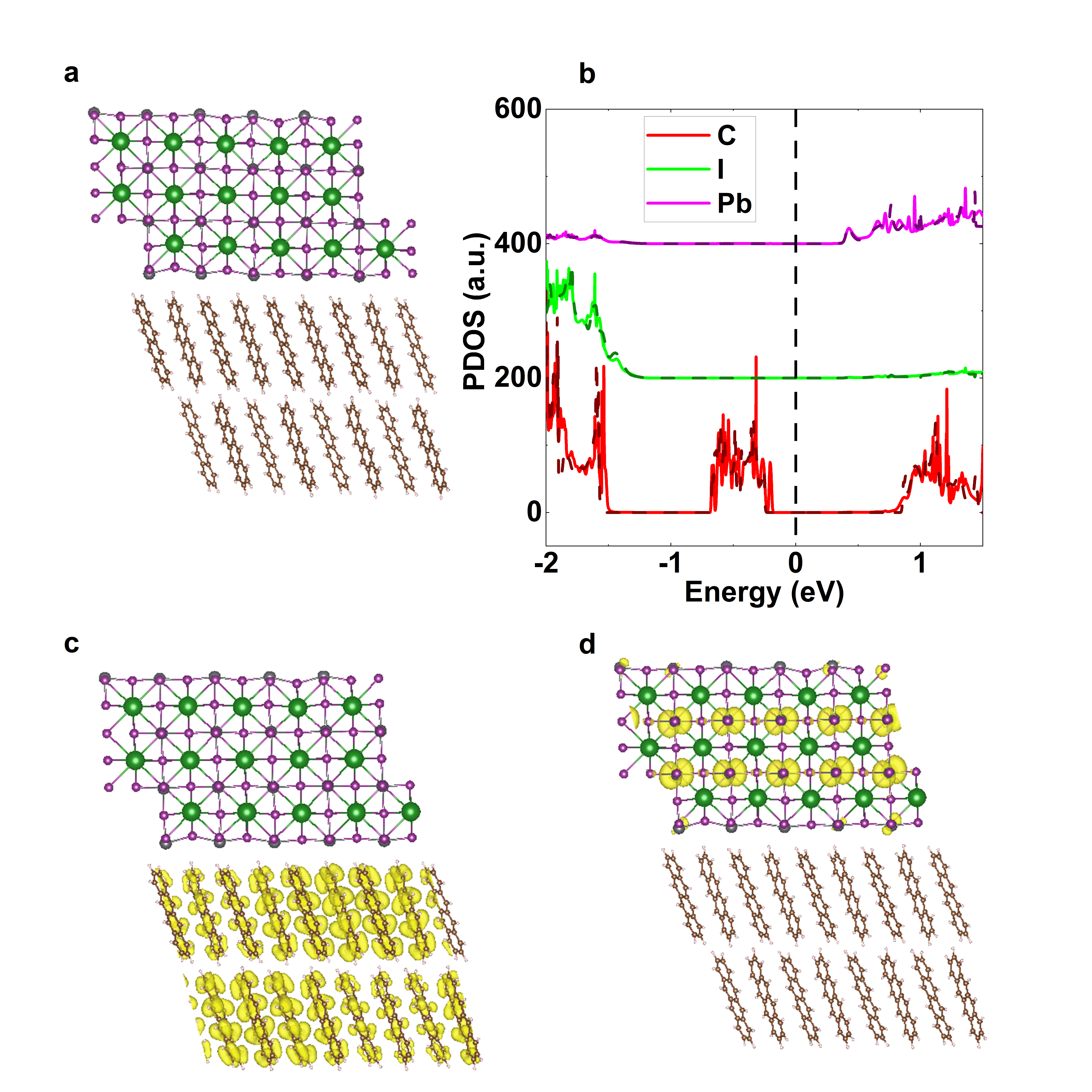
We ran geometry relaxations for all simulation cells. All cuts ran successfully except cut 2 with CsI termination, where the halide perovskite structure fell apart during computation. We attribute this to the unit cell being too strained for the optimisation to complete and this geometry is not discussed further. We present a relaxed geometry in Figure 4a for PbI2 terminated cut 1 no rotation. In all cut 1 configurations, including that presented here, we found tetracene molecules to be almost entirely unchanged in position from a thin film of tetracene. For cut 2, we found the spacing between tetracene molecules reduced slightly (< % change) in the non-periodic direction, especially for molecules adjacent to the interface. In all cases the halide perovskite surface distorted more significantly.
We define the interface formation energy per tetracene molecule as
| (1) |
where is the number of tetracene molecules in the interface simulation. The factor of two arises from the double interface. We present formation energies in Table 2. Larger energy reductions are observed for CsI termination, which is explained by noting that bare CsI surfaces are less stable (higher in energy) than the PbI2 surfaces, so bulk films provide more significant stabilisation. In both cases the two cut 1 geometries have almost identical energies, suggesting that tetracene’s orientation on the halide perovskite surface is only weakly dependant on the halide perovskite. This is indicative of weak interaction between the two materials. For PbI2 termination, we find cut 1 orientations are more favourable than cut 2, as is again expected for rod-like molecules Hlawacek and Teichert (2013). All formation energies are significantly higher than for bulk tetracene ( eV per molecule) which suggests tetracene will not bind strongly to the halide perovskite surface. It may instead form pillars or other structures with only small contact regions with the halide perovskite, as seen in our experimental section (c.f. supplementary information Figure 6b) and has been discussed by others Hlawacek and Teichert (2013).
| Tetracene orientation | (eV) |
|---|---|
| CsI termination | |
| Cut 1 no rotation | |
| Cut 1 with rotation | |
| PbI2 termination | |
| Cut 1 no rotation | |
| Cut 1 with rotation | |
| Cut 2 |
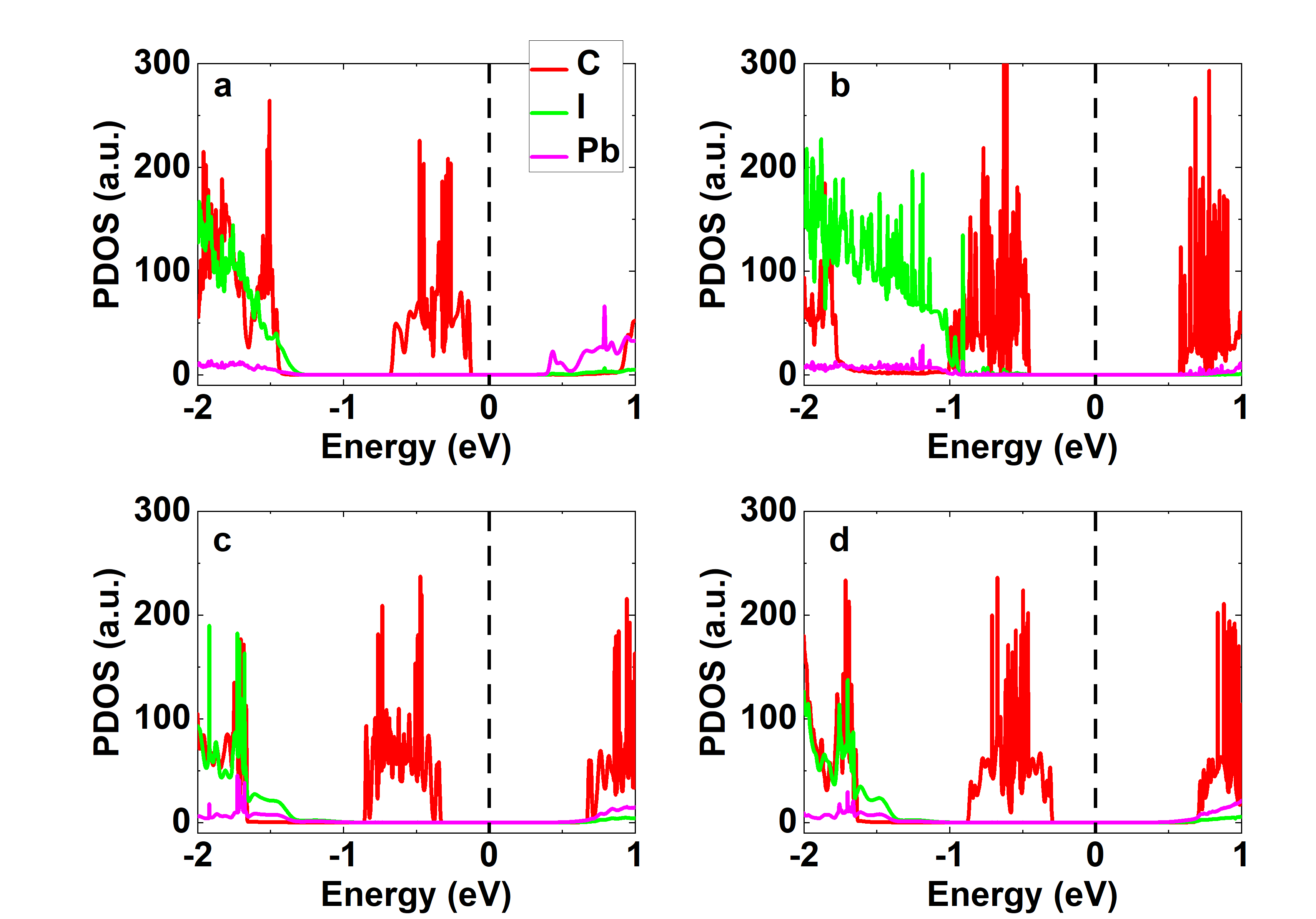
We show the projected density of states for PbI2 terminated cut 1 no rotation in Figure 4b (PDOS for other cut 1 simulations are presented in supplementary information Figure 10). As in the case of a single molecule, tetracene’s valence band is located above the halide perovskite’s. This was the case for all other simulations. Overlaid on this plot in dashed lines are the PDOS for halide perovskite and tetracene slabs (independently) isolated in a vacuum. For the halide perovskite, the isolated PDOS overlaps almost perfectly with the valence and conduction bands. We find tetracene’s PDOS at the interface is slightly broadened with respect to isolated tetracene, which we attribute to each tetracene molecule being in a slightly different electronic environment at the interface. This PDOS demonstrates there is little interaction between the halide perovskite and tetracene, as their states can be well reproduced by isolated slabs.
We present the valence and conduction band charge densities (at the band edge) for cut 1 no rotation, for PbI2 termination, in Figure 4c and d respectively. Both charge densities are isolated to one material only (tetracene and halide perovskite respectively), again implying that there is little change in electronic states at the interface. When looking further into the valence band (at the k-point corresponding to the valence band maximum), no states are found are found to have significant charge density in both the halide perovskite and the tetracene.
VIII Toy interface with exciton visualisation
To model triplet excitons it is necessary to solve the Bethe-Salpeter equation. We attempted this on the full interfaces presented in the previous section, but found it was not computationally feasible. A similar limitation was recently highlighted in Janke and co-workers’ study of pentacene and tetracene on passivated silicon surfaces Janke et al. (2020). Other studies have focused on the development of fragment-based (post-DFT) and BSE calculations, allowing for modelling of interfaces Bethe et al. (2020). However, in fragment-based approaches the exchange interaction needs to be neglected, meaning singlet and triplet states cannot be differentiated.
Despite these limitations, we decided to carry out highly speculative calculations to explore what excitonic properties can be modelled at an interface with modern computational methods and resources. We note it is unclear whether full excitonic states will form at the interface, or whether charges dissociate prior to reaching the interface, but here we aim to increase understanding of the possible states at the interface and ascertain what current computational methods reveal. To this end we constructed small toy interfaces consisting of a single tetracene unit cell and a single (in plane) CsPbI3 unit cell. In these models we oriented tetracene perpendicular to the interface (cut 1 orientation, as this was the most energetically favourable) and the halide perovskite again had three repeating units in the non-periodic direction. As we are interested primarily in tetracene’s electronic states, the model’s in plane lattice parameters were constrained to those of tetracene. To achieve this, one of the halide perovskite’s in plane lattice parameters was increased by 20 % and the other reduced by 3 %. Again we modelled both CsI and PbI2 terminations. We carried out geometry optimisations (with in plane lattice parameters constrained) without any vacuum spacing. However, for and BSE calculations the lack of vacuum spacing resulted in interaction between adjacent unit cells in the non-periodic direction. Therefore, we introduced a vacuum layer (the same size as the ‘filled’ unit cell) and used a Coulomb cutoff to prevent long-range interactions between repeating unit cells.
We calculated the PDOS of these small models (with vacuum spacing) and our results are presented in supplementary information Figure 11a and b. Electronic states were positioned similarly to those presented in previous sections, with the same atomic orbitals contributing to the halide perovskite’s valence and conduction bands, and tetracene’s valence band being above that of the halide perovskite. Importantly, we found the halide perovskite’s bandgap had increased, due to the larger in plane lattice parameter increasing quantum confinement. Density of states calculations including spin-orbit coupling, plotted in supplementary information Figure 11c and d, demonstrate that for PbI2 termination there is no bandgap in this system, preventing post-DFT calculations with spin-orbit coupling on this system.
We were able to carry out and BSE calculations on these toy interface models. However, further simplifications were needed for calculations to proceed: we neglected the non-local commutator and we reduced the maximum reciprocal lattice vector size with respect to DFT calculations. The latter approximation is equivalent to reducing the cutoff energy in a DFT calculation, but was found to have only small effect (< eV) due to smaller reciprocal lattice grids being required in calculations (see supplementary information C). We found both approximations were reasonable by carrying out one calculation without these approximations - minimal difference in results was observed.
calculations on the toy interfaces, alongside on just tetracene and toy halide perovskite, allow for an estimation of the changes that would occur to the PDOS calculations already presented. Specifically, we present corrections in supplementary information Table 6, focusing on the change in energy offset between halide perovskite and tetracene valence bands. In general our results point towards the difference in energy between the halide perovskite and tetracene valence bands being larger than what was calculated at DFT-level by 1 eV. As was discussed in section V, this would be partly offset by calculations including spin-orbit coupling in the halide perovskite (reducing energy difference between the halide perovskite and tetracene valence bands), so we consider that the PDOS presented above give the correct qualitative conclusions.
We plot DFT energies versus energies for valence and conduction bands in Figure 5a and b for CsI terminated toy model with spin-orbit coupling. Unlike in most situations, corrections to DFT-level energies do not form straight lines. This is because the halide perovskite and tetracene energy corrections are significantly different in magnitude (as tetracene’s electronic states are more localised). Furthermore, there are some mixed states including both part of the tetracene and halide perovskite wavefunction which carry intermediate energy corrections. To model tetracene’s electronic states correctly at the interfaces, we fit a straight line to states where the DFT wavefunction is fully localised on tetracene, as shown on the figure. These fits allow for a comparison of tetracene’s level bandgap with that of bulk tetracene and isolated tetracene sheets (cut 1). We present results in supplementary information Table 7. Tetracene’s level bandgap is lowered at all interfaces, which is attributed to the halide perovskite stabilising single particle excited states in tetracene.
We show a schematic of energy levels in the toy model interfaces in Figure 5c. The only states close to the Fermi level are tetracene’s valence band and the halide perovskite’s conduction band. We define the energy difference between these states as . This means we can explore exciton dissociation at the interface, but not full exciton transfer.
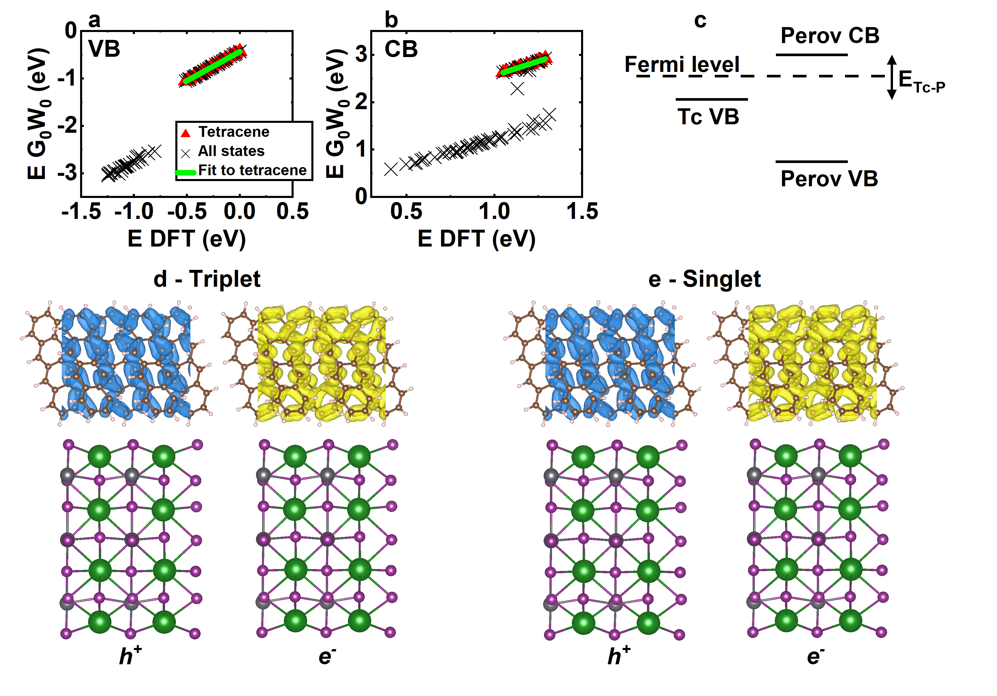
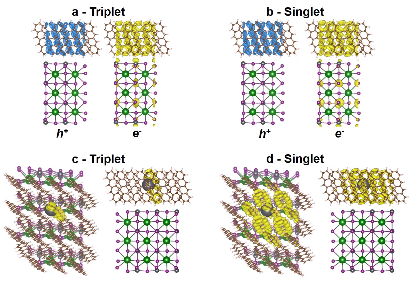
To carry out BSE (exciton) calculations, we applied scissor corrections to DFT energy levels. Scissor corrections shift DFT-level valence and conduction band states by constant gradients, as in the red lines on Figure 5a and b, and add a constant value to the DFT-level bandgap. Initially, we used the scissor corrections found from fits i.e. correctly replicating tetracene’s electronic states at the interface (as in Figure 5a and b). With these scissor corrections, for both CsI and PbI2 terminated surfaces, we found tetracene’s triplet state to be the lowest energy state at the interface. In calculations including spin-orbit coupling we identified ‘triplet’ and ‘singlet’ states as triply/singly degenerate dark/bright states with significant electron and hole contributions on tetracene. At both interfaces we found the singlet and triplet energies to be extremely comparable to those of a tetracene cut 1 layer in a vacuum (see supplementary information Table 7). For example, for CsI termination with spin-orbit coupling, we found the triplet states at eV, while for the same tetracene geometry in a vacuum (i.e. no halide perovskite present) a triplet energy of eV was calculated, in agreement within calculation error. This is indicative of tetracene’s excitonic states being relatively unaffected by the presence of the halide perovskite.
We plot the average hole and electron positions of the lowest energy triplet and singlet states for CsI termination in Figure 5d and e respectively (with scissor correction applied which correctly reproduces tetracene’s electronic states). Both states are found to be strongly localised to tetracene. Specifically, for both triplet and singlet there is less than a 3 % probability of the electron or hole being within the halide perovskite. Importantly, there are lower energy charge transfer states than the singlet state in this model where the electron is fully localised on the halide perovskite. We present equivalent results for PbI2 terminated surfaces in supplementary information I. Again we calculate well formed singlet and triplet states localised on tetracene only.
Figure 5 was in the case of being larger than tetracene’s triplet energy. To explore excitonic states in the presence of lower energy states available, we then slightly altered the scissor correction, reducing and making charge transfer states (with the electron localised on the halide perovskite and the hole on the tetracene) lower in energy than tetracene’s triplet energy (see supplementary information Table 8). We obtained almost identical results: singlet and triplet states remain strongly localised on tetracene at the interface when there are lower energy states available. Furthermore, for charge transfer states, the electron/hole remained fully localised on the halide perovskite/tetracene. Our results therefore suggest one possible issue for exciton dissociation is the spatial separation of relevant states.
Changing the scissor correction means tetracene’s electronic states are no longer exactly reproduced fully at the interface. As a final confirmation to show that results with altered scissor corrections are valid, we replaced lead with tin to form an SnI2 terminated surface. Following geometry relaxations, we carried out the same and BSE calculations. We obtained charge transfer states lower in energy than tetracene’s triplet energy for the physically correct scissor shift. Importantly, our results were found to be similar to those for the PbI2 discussed in supplementary information I, with triplet states remaining localised on tetracene. This confirms that results calculated with approximate scissor corrections are valid.
We attempted to extend these calculations by further altering the scissor correction, reducing the halide perovskite’s bandgap to less than tetracene’s triplet energy. This required extreme scissor corrections and only resulted in charge transfer states (with electron localised on the halide perovskite only). No conclusions can be drawn from this as nothing resembling a singlet or triplet state was calculated. We anticipate this is due to the extreme scissor correction meaning tetracene’s electronic states were not well reproduced.
In summary, we find tetracene’s triplet and singlet states are strongly localised to tetracene at all interfaces considered. Furthermore, singlet and triplet energies are comparable to those for tetracene isolated in a vacuum for all interfaces. These combined results suggest that, for the optimal orientation of tetracene on the halide perovskite, tetracene’s excitonic states still exist at the interface and are relatively unaffected by the presence of an inorganic semiconductor.
IX Conclusion
We have presented a study of the interface between singlet fission materials and halide perovskites. This study was motivated by 150 experiments screening for triplet transfer from a singlet fission material to a halide perovskite. In our model we found tetracene behaved in a broadly similar way to other organic/inorganic interfaces where the organic is a rod like structure: lone organic molecules orient parallel to the halide perovskite surface, while films orient with the long axis perpendicular to the surface. In all cases we found interface formation energies were much less favourable than for bulk tetracene and tetracene’s valence band was higher energy than the halide perovskite’s valence band, suggestive of tetracene being a good hole transporter. In general we observed only weak electronic interaction between these two materials. By using small models, we were able to calculate the excitonic states between tetracene and a toy halide perovskite-like structure. We found singlets and triplets remain localised on tetracene molecules at the interface and tetracene’s excitonic energies were unaffected by the presence of the halide perovskite. Our results are indicative of only weak interaction between tetracene’s excitonic states and an inorganic semiconductor (for optimal molecular arrangements at the interface). We suggest future work should focus on increasing electronic interaction at the interface by further exploring chemical bonding between the two materials, improving interface formation energies and increasing the probability of triplet transfer. Our work lays the ground for achieving triplet transfer from a singlet fission material to a halide perovskite.
Acknowledgements.
A.R.B. acknowledges funding from a Winton Studentship, Oppenheimer Studentship and the Engineering and Physical Sciences Research Council (EPSRC) Doctoral Training Centre in Photovoltaics (CDT-PV). A.R.B. thanks all the support from the Yambo community forum, especially Daniele Varsano. A.R.B. acknowledged Matthew Klug, Rohit Prasanna, Thomas Feurer and Edoardo Ruggeri for fabrication of low-bandgap halide perovskites and copper indium gallium selenide thin films. S.D.S. acknowledges the Royal Society and Tata Group (UF150033) and the EPSRC (EP/R023980/1, EP/T02030X/1, EP/S030638/1). B.M. acknowledges support from the Gianna Angelopoulos Programme for Science, Technology, and Innovation and from the Winton Programme for the Physics of Sustainability. This work was performed using resources provided by the Cambridge Service for Data Driven Discovery (CSD3) operated by the University of Cambridge Research Computing Service (www.csd3.cam.ac.uk), provided by Dell EMC and Intel using Tier-2 funding from the Engineering and Physical Sciences Research Council (capital grant EP/P020259/1), and DiRAC funding from the Science and Technology Facilities Council (www.dirac.ac.uk). The data underlying this manuscript are available at [url to be added in proof]. S.D.S. is a Co-Founders of Swift Solar Inc.Appendix A List of experiments undertaken screening for triplet transfer
Experiments break down into two types: evaporation and solution processing. Tetracene and DPH were purchased from Sigma at the highest purity available (> 99.99 %, > 98 % and > 95 % respectively). All samples were fabricated on glass, which was cleaned in ultrasonic baths of acetone and then isopropanol prior to fabrication. All fabrication was carried out in nitrogen filled gloveboxes with oxygen levels of less than 10 ppm and water levels of less than 0.1 ppm. All samples were encapsulated immediately following fabrication, either by a two part or UV cured epoxy (Bluefixx). Halide perovskites marked ‘in situ’ were fabricated by the author, with other samples supplied by Rohit Prasanna and Matthew Klug Prasanna et al. (2017); Klug et al. (2016) (see section A.2 for fabrication details). In all cases no triplet transfer was observed.
In general we found it was not straightforward to form a smooth interface between these materials, independent of the deposition method used. Instead, the two materials tended to separate, for example via the growth of pillars of the singlet fission material in evaporation (as in supplementary information Figure 6b). While some solution processing methods allowed for smooth bilayer outer surfaces, it was still unclear whether a smooth interface between the two materials had been achieved.
A wide parameter space for singlet fission material deposition was explored by using:
-
1.
evaporation of the organic on the halide perovskite, with evaporation rates from 0.5 Å to 17 Å and deposition thicknesses from 7.5 nm to 150 nm
-
2.
spin coating the organic on the halide perovskite, with singlet fission materials dissolved in chlorobenzene (which halide perovskites are not soluble in), spinning speeds from 2000 to 4000 rotations per minute and sample annealing times from 0 to 30 minutes (prior to encapsulation)
-
3.
drop casting the organic on the halide perovskite, with different solution concentrations deposited (though this resulted in extremely thick organic films in all cases, so was not significantly investigated)
-
4.
spin-coating the halide perovskite on singlet fission materials (noting this resulted in much of the singlet fission material being removed from the substrate)
-
5.
spin-coating the singlet fission material and halide perovskite at once to attempt to form heterojunctions.
Full details of deposition conditions are now briefly listed.
A.1 Evaporation
All evaporations were carried out at a pressure of 1 10-5 mbar or lower. Tetracene was evaporated at a temperature of 120∘C, DPH at110∘C, CBP at 190∘C and C60 at 400∘C. Note for DPH evaporations thicknesses and evaporation rates are nominal as tetracene tooling factors were used. DPH is a heavier molecule so these should be regarded as upper bounds.
-
1.
30 nm of tetracene was evaporated at a rate of 0.5 Ås-1 on FAPb0.5Sn0.5I3 samples, with a small proportion of the lead and tin replaced with =0 %, 2 %, 5 % and 10 % Ca, Mg, Sr, Zn, Co and Ni (where is defined as in Bowman and co-workers Bowman et al. (2019)). Halide perovskite samples were 200 nm thick.
-
2.
30 nm of tetracene was evaporated at a rate of 0.5 Ås-1 on =0 %, 2 % and 10 % Mg, Sr and Co samples. Halide perovskite samples were 200 nm thick.
-
3.
60 nm of tetracene was evaporated at a rate of 1 Ås-1 on =0 %, 2 % and 10 % Co and Zn samples. Halide perovskite samples were 200 nm thick.
-
4.
60 nm of tetracene was evaporated at a rate of 0.7 Ås-1 on MAyFA1-ySn0.75Pb0.25I3 samples, with =0, 0.2, 0.4, 0.6, 0.8 and 1. Halide perovskite samples were a range of thicknesses around 300 nm.
-
5.
150 nm of DPH was evaporated at a rate of 0.5 Ås-1 on =0 %, 2 %, 5 % and 10 % Zn samples. Halide perovskite samples were 200 nm thick.
-
6.
20/150/150 nm of DPH was evaporated at a rate of 0.5/0.8/7.0 Ås-1 on 200 nm thick CszFA1-zSn0.5Pb0.5I3 with =0, 0.05, 0.1, 0.15 and 0.2, for =0 % and 5 % Zn.
-
7.
150 nm of DPH was evaporated at a rate of 6.5/0.5/2.5/17 Ås-1 on 100 nm thick CszFA1-zSn0.75Pb0.25I3, = 0, 0.05, 0.1, 0.15, 0.2, MAyFA1-ySn0.75Pb0.25I3, =0.4, 0.8, 1.0 and in situ fabricated FA0.75Cs0.25Sn0.75Pb0.25I3.
-
8.
5.2 nm of C60 was evaporated on MAyFA1-ySn0.75Pb0.25I3 with =0, 0.8 and 1 at a rate of 0.4 Ås-1 (as C60 is known to separate triplets from singlet fission materials). On these samples, and equivalent samples samples without C60 deposited, 5/50/500/500 nm of DPH/DPH/tetracene/DPH was evaporated at a rate of 15 Ås-1 (noting that higher evaporation rates had been observed to reduce the formation of pillars). Halide perovskites were 100 nm thick.
-
9.
=0 % and =5 % Zn samples of 200 nm and 50-100 nm thicknesses had either DPH, or DPH followed by CBP evaporated on them. For the former, 100 nm of DPH was evaporated at 1 Ås-1, while for the latter 7.5 nm DPH was evaporated at 1.2 Ås-1 followed by 100 nm CBP at 1 Ås-1. This was with the suggestion of transferring singlet excitons from a high-bandgap absorber (CBP) to a thin layer of singlet fission material (DPH).
-
10.
7.5 nm of DPH was evaporated at a rate of 5 Ås-1 on 500 nm and 100 nm thickness FASn0.75Pb0.25I3 and MASn0.75Pb0.25I3 samples. On half of these samples (four of each were made) 200 nm of CBP was evaporated at a rate of 1.2 Ås-1, again with the suggestion of transferring singlet excitons from a high-bandgap absorber (CBP) to a thin layer of singlet fission material (DPH).
A.2 Solution processing
All solution processing was carried out in nitrogen filled gloveboxes with < 10ppm O2 and < 1ppm H2O.
All ‘in situ’ fabricated low-bandgap FA0.75Cs0.25Sn0.75Pb0.25I3 halide perovskites samples were fabricated from stock solutions of PbI2 (0.28 M), SnI2 (0.83 M), SnF2 (0.16 M), FAI (0.83 M) and CsI (0.28 M) in a 65:35 solution of DMF:DMSO (all Sigma). In all cases films were spin coated: 30 L of the solution was deposited on a substrate which was spun at 4000 rotations per minute for 30 s, with a gas quench applied from 15 s. Samples were annealed at 100∘C for 15 minutes. Solution processed experiments undertaken are as follows:
-
1.
A stock solution for in situ fabrication was diluted to 10 % of normal concentration and low-bandgap halide perovskites were deposited (achieving very thin films). 0.03/0.07/0.18 M DPH in chlorobenzene was prepared at 25/50/80∘C and statically deposited on the halide perovskite. Four of each sample were made, half of which were spun at 1000 rotations per minute for 20 s (i.e. spin-coating and drop casting was carried out). One of each sample type was annealed at 100∘C for 15 minutes while the others were left to air dry.
-
2.
Bulk heterojunctions were spin-coated in situ. A FA0.75Cs0.25Sn0.75Pb0.25I3 precursor solution was split into four. The first was used as a control solution, the second had 0.04 M DPH dissolved into it (DPH’s solubility limit in these solutions at room temperature), the third was diluted by 50 % and then had 0.04 M DPH dissolved into it and the last was heated to 70∘C and had 0.13 M DPH dissolved into it.
Appendix B Other experimental methods
B.1 Atomic force microscopy
Atomic force microscopy (AFM) was carried out using an Asylum Research MFP-3D atomic force microscope in non-contact AC mode. 0th order flattening and 1st order plane fits were applied to all data. All measurements and data processing were carried out on Asylum Research AFM Software version 15.
B.2 Photoluminescence
In photoluminescence measurements samples were excited by a continuous wave temperature controlled Thorlabs 405 nm laser. The emission was recorded using an Andor IDus DU420A silicon detector for lead-only samples or and an Andor IDus DU490A InGaAs detector.
B.3 Time resolved photoluminescence
Time-resolved PL spectra were recorded using a gated intensified CCD camera (Andor iStar DH740 CCI-010) connected to a calibrated grating spectrometer (Andor SR303i). A Ti:sapphire optical amplifier (1 kHz repetition rate, 90 fs pulse width) was used to generate narrow bandwidth photoexcitation (20 nm full-width at half maximum) with a wavelength of 400 nm, via a custom-built noncollinear optical parametric amplifier.
Appendix C Computational details
We carried out geometry optimisations with the density functional theory (DFT) code CASTEP Clark et al. (2005) with on-the-fly generated ultra-soft pseudopotentials. Spin-orbit coupling was not included in our geometry optimisations as we found it had a small effect relative to the additional computational effort: the lattice parameter of cubic CsPbI3 only changed from Å to Å with the inclusion of spin-orbit coupling. We used a cutoff energy of eV in all geometry optimisations. Van der-Waals semi-empirical corrections were required for all calculations to correctly reproduce tetracene’s geometry and electronic structure, as is discussed further in section IV. For primitive tetracene and halide perovskite unit cells we used a Monkhorst-Pack -point grid of , while for larger cells (e.g. two repeating tetracene and three repeating halide perovskite units in the non-vacuum direction) we used a commensurate reduced number of -points in periodic directions (with a minimum of 2 -points being used in these directions), while in the non-periodic direction only the point was sampled. In all supercells with a vacuum, we converged the vacuum size to be large enough to not affect results. This corresponded to a vacuum at least 0.8 times the size of the unit cell for CsPbI3 and at least the same length as the unit cell size for tetracene. The same cutoff energies and -point grids were used for density of states (DOS) and projected-DOS (PDOS) calculations. For density of states calculations including spin-orbit coupling we used a cutoff energy of eV, a Monkhorst-Pack -point grid of for SCF calculations, a Monkhorst-Pack -point grid of for spectral calculations and CASTEP’s norm-conserving pseudopotentials. For calculations of a tetracene molecule on a halide perovskite surface we fixed the lattice parameters, while for thin-film interfaces lattice parameters were allowed to vary freely (discussed further in section VI and VII).
We used the DFT code Quantum Espresso and post-DFT code Yambo to calculate electronic and excitonic statesGiannozzi et al. (2009, 2017); Marini et al. (2009). In Quantum Espresso we used -point grids of (so the and R points were both directly sampled), with a cutoff energy of eV ( Ry). Norm-conserving Vanderblit pseudopotentials, taken from the Schlipf-Gygi norm-conserving pseudopotential library, were employed in these computations as they are optimised for subsequent Yambo calculationsHamann (2013); Schlipf and Gygi (2015); Scherpelz et al. (2016). In all our Yambo calculations, parameters were converged to give results to an accuracy of at least eV. To aid with Yambo calculations at full interfaces, we sometimes ignored the non-local commutator (noted in text), which was found to affect calculations on tetracene and halide perovskite only minimally (changing energies by < eV), and for toy models we reduced the maximum size of reciprocal lattice vectors (corresponding to the cut-off energy used in DFT calculations) with respect to that in Quantum Espresso calculations (which affected the accuracy of calculations to < 0.01 eV).
Appendix D Functional choice
Geometry optimisations of tetracene were carried out with several functionals to assess which best reproduced experimental lattice parameters. Results are summarised in Table 3. We note that for PBE and PBEsol functionals the lattice expanded well beyond what would be physically reasonable, and did not lead to a relaxed geometry, without a van der Waals correction.
| Functional | Lattice parameter |
|---|---|
| Experimental Campbell, Robertson, and Trotter (1962) | |
| (no temperature stated, | |
| assumed room temperature) | |
| LDA | |
| Summed difference with experiment | 1.24 |
| PBE + TS | |
| Summed difference with experiment | 0.60 |
| PBE + G06 Grimme (2006) | |
| Summed difference with experiment | 2.05 |
| PBE + JCHS Jurecka et al. (2007) | |
| Summed difference with experiment | 3.41 |
| PBESOL + TS | |
| Summed difference with experiment | 1.12 |
Appendix E Bulk CsPbI3
Iodine and lead are the main contributors to the valence and conduction bands in experimental halide perovskites at room temperature Haruyama et al. (2014). However, in the fully relaxed cubic CsPbI3, we found the nature of the valence and conduction bands is inverted at the DFT-level when including spin-orbit coupling (when using PBE with TS correction). We found increasing the halide perovskite’s lattice parameter by 2 % or more allows for correct band ordering at the DFT-level (with iodine/lead being the main contributor to the valence/conduction band), as plotted in Figure 8 a and b.
We carried out a one shot correction to the cubic halide perovskite’s band structure. While corrections do not give halide perovskites’ bandgaps with full accuracy, calculations beyond are too computationally intensive to carry out when modelling interfaces Filip and Giustino (2014); Leppert, Rangel, and Neaton (2019). In order to have correct band ordering for calculations, we carried out calculations on structures with the lattice parameter 2 % to 5 % larger than the relaxed structure. The DFT- and -level bandgaps for these cells (with spin-orbit coupling) are shown in Figure 8c. From these results we extrapolated the approximate bulk bandgap of relaxed CsPbI3 as 0.98 eV. This is close to the DFT-level bandgap without spin-orbit coupling of 1.09 eV, suggesting the halide perovskite’s electronic structure without spin-orbit coupling approximately models results from post-DFT methods with spin-orbit coupling included. We use this to approximately model electronic states at interfaces in subsequent sections (and calculate approximate errors associated with this).
Appendix F Halide perovskite lattice sizes with a different number of repeating units in the vacuum direction
We present inter-atomic distances for geometry relaxed halide perovskite slabs with different numbers of periodic units in the vacuum direction in Table 4. Specifically, we present the inter-atomic distance in the centre of the structure, in the vacuum direction, for both Cs-Cs and Pb-I distances, alongside the lattice parameter in a direction perpendicular to the vacuum. We note that the relaxed bulk cubic lattice parameter is Å.
| Number of repeating units | Pb-I | Cs-Cs | Perpendicular lattice parameter |
| CsI termination | |||
| 1 | |||
| 2 | |||
| 3 | |||
| 4 | |||
| 5 | |||
| 7 | |||
| 8 | |||
| PbI2 termination | |||
| 1 | N/A | ||
| 2 | |||
| 3 | |||
| 4 | |||
| 5 | |||
| 6 | |||
| 7 | |||
| 8 |
Appendix G Commensurate unit cells
We present the commensurate unit cells for halide perovskite and tetracene films in Figure 9. The corresponding normal and shear strains for each arrangement are presented in Table 5.
| CsI termination | PbI2 termination | |
|---|---|---|
| Cut 1 no rotation | ||
| Strain in x direction (%) | ||
| Strain in y direction (%) | ||
| Shear strain (%) | ||
| Cut 1 with rotation | ||
| Strain in x direction (%) | ||
| Strain in y direction (%) | ||
| Shear strain (%) | ||
| Cut 2 | ||
| Strain in x direction (%) | ||
| Strain in y direction (%) | ||
| Shear strain (%) |
Appendix H G0W0 for different tetracene/halide perovskite electronic states and scissor corrections
The effect of G0W0 corrections of different isolated tetracene and halide perovskite models, and small interfaces, are presented in Table 6. All models presented are in approximate agreement, with the tetracene valence band being increased in energy by eV more than the halide perovskite valence band following a G0W0 correction, and the tetracene conduction band being increased by at least eV more than the halide perovskite conduction band.
For the CsI terminated toy model, the offset between the halide perovskite and tetracene’s valence band is eV without spin-orbit coupling and eV with spin-orbit coupling. This suggests (alongside the results in Table 6) that the qualitative results drawn from PDOS calculations in sections VI and VII (without spin-orbit coupling) would still be valid with the inclusion of spin-orbit coupling and subsequent G0W0 corrections, with tetracene valence band state being further increased in energy with respect to the halide perovskite valence band state.
We present tetracene’s G0W0 bandgap, singlet and triplet energies for the toy interfaces, bulk tetracene and tetracene in a vacuum in Table 7. There are three models for tetracene in a vacuum – geometry relaxed, and the same geometries as used at both PbI2 and CsI terminated toy models. Finally, we present scissor shifts applied in the main text in Table 8.
| Model | (eV) | (eV) |
|---|---|---|
| Bulk systems (no SO) | ||
| Bulk systems (with SO) | ||
| Bulk P and Tc in vacuum (no SO) | ||
| Bulk P and Tc in vacuum (with SO) | ||
| CsI terminated toy model (no SO) | ||
| CsI terminated toy model (with SO) | ||
| PbI2 terminated toy model (no SO) |
| Model | (eV) | (eV) | (eV) |
|---|---|---|---|
| Bulk tetracene | |||
| Tetracene in vacuum (relaxed) | |||
| Tetracene in vacuum (CsI toy geometry) | |||
| Tetracene in vacuum (PbI2 toy geometry) | |||
| CsI terminated toy model (no SO) | |||
| CsI terminated toy model (with SO) | |||
| PbI2 terminated toy model (no SO) |
| Model | (eV) | ||
|---|---|---|---|
| CsI termination | |||
| Physically correct scissor correction | |||
| Alternative scissor correction | |||
| PbI2 termination | |||
| Physically correct scissor correction | |||
| Alternative scissor correction |
Appendix I G0W0 calculations for PbI2 terminated surfaces
In Figure 12a and b we plot average exciton electron and hole position for PbI2 termination (for lowest energy triplet and singlet states). Here the average electron wavefunctions are found to have a small contribution within the halide perovskite (noting isosurfaces are only on tetracene up to the 88 % probability surface). However, within our simulations tetracene makes up only a small region of the simulation cell and therefore there are contributions to the average electron position both from the hole being in vacuum and on the halide perovskite. To this end, we plot the electron charge density in Figure 12c and d for the hole (grey sphere) fixed on a tetracene molecule. These plots reveal that when the hole is fixed on a tetracene molecule, the electron also is. We observed this for the hole being fixed at many different locations within tetracene. These results again demonstrate that tetracene’s excitonic states are strongly localised, even at an interface. This is also suggestive that electrons in the halide perovskite may transfer into tetracene and then become localised within the organic.
Appendix J Additional supplementary information figures


References
- Yadav et al. (2017) P. Yadav, K. Pandey, V. Bhatt, M. Kumar, and J. Kim, “Critical aspects of impedance spectroscopy in silicon solar cell characterization: A review,” Renew. Sustain. Energy Rev. 76, 1562–1578 (2017).
- Martha et al. (2009) S. K. Martha, E. Markevich, V. Burgel, G. Salitra, E. Zinigrad, B. Markovsky, H. Sclar, Z. Pramovich, O. Heik, D. Aurbach, I. Exnar, H. Buqa, T. Drezen, G. Semrau, M. Schmidt, D. Kovacheva, and N. Saliyski, “A short review on surface chemical aspects of Li batteries: A key for a good performance,” J. Power Sources 189, 288–296 (2009).
- Yang, Dou, and Wang (2018) Z. Yang, J. Dou, and M. Wang, “Interface Engineering in n-i-p Metal Halide Perovskite Solar Cells,” Sol. RRL 2, 1–16 (2018).
- Andaji-Garmaroudi et al. (2020) Z. Andaji-Garmaroudi, M. Abdi-Jalebi, F. U. Kosasih, T. Doherty, S. Macpherson, A. R. Bowman, G. J. Man, U. B. Cappel, H. Rensmo, C. Ducati, R. H. Friend, and S. D. Stranks, “Elucidating and Mitigating Degradation Processes in Perovskite Light-Emitting Diodes,” Adv. Energy Mater. 2002676, 2002676 (2020).
- Stadlober et al. (2006) B. Stadlober, U. Haas, H. Maresch, and A. Haase, “Growth model of pentacene on inorganic and organic dielectrics based on scaling and rate-equation theory,” Phys. Rev. B - Condens. Matter Mater. Phys. 74, 1–9 (2006).
- DeQuilettes et al. (2016) D. W. DeQuilettes, S. Koch, S. Burke, R. K. Paranji, A. J. Shropshire, M. E. Ziffer, and D. S. Ginger, “Photoluminescence Lifetimes Exceeding 8 s and Quantum Yields Exceeding 30 % in Hybrid Perovskite Thin Films by Ligand Passivation,” ACS Energy Lett. 1, 438–444 (2016).
- Zhang et al. (2015) Y. Zhang, M. Liu, G. E. Eperon, T. C. Leijtens, D. McMeekin, M. Saliba, W. Zhang, M. de Bastiani, A. Petrozza, L. M. Herz, M. B. Johnston, H. Lin, and H. J. Snaith, “Charge selective contacts, mobile ions and anomalous hysteresis in organic–inorganic perovskite solar cells,” Mater. Horiz. 2, 315–322 (2015), arXiv:9605103 [cs] .
- Smith and Michl (2010) M. B. Smith and J. Michl, “Singlet Fission,” Chem. Rev. 110, 6891–6936 (2010).
- Tayebjee, McCamey, and Schmidt (2015) M. J. Y. Tayebjee, D. R. McCamey, and T. W. Schmidt, “Beyond Shockley–Queisser: Molecular Approaches to High-Efficiency Photovoltaics,” J. Phys. Chem. Lett. 6, 2367–2378 (2015).
- Scholes (2003) G. D. Scholes, “Long-Range Resonance Energy Transfer in Molecular Systems,” Annu. Rev. Phys. Chem. 54, 57–87 (2003).
- Dexter (1953) D. L. Dexter, “A Theory of Sensitized Luminescence in Solids,” J. Chem. Phys. 21, 836 (1953).
- Piland et al. (2014) G. B. Piland, J. J. Burdett, T. Y. Hung, P. H. Chen, C. F. Lin, T. L. Chiu, J. H. Lee, and C. J. Bardeen, “Dynamics of molecular excitons near a semiconductor surface studied by fluorescence quenching of polycrystalline tetracene on silicon,” Chem. Phys. Lett. 601, 33–38 (2014).
- Macqueen et al. (2018) R. W. Macqueen, M. Liebhaber, J. Niederhausen, M. Mews, C. Gersmann, S. Jäckle, K. Jäger, M. J. Tayebjee, T. W. Schmidt, B. Rech, and K. Lips, “Crystalline silicon solar cells with tetracene interlayers: The path to silicon-singlet fission heterojunction devices,” Mater. Horizons 5, 1065–1075 (2018).
- Tabachnyk et al. (2014) M. Tabachnyk, B. Ehrler, S. Gélinas, M. L. Böhm, B. J. Walker, K. P. Musselman, N. C. Greenham, R. H. Friend, and A. Rao, “Resonant energy transfer of triplet excitons from pentacene to PbSe nanocrystals,” Nat. Mater. 13, 1033–1038 (2014).
- Thompson et al. (2014) N. J. Thompson, M. W. B. Wilson, D. N. Congreve, P. R. Brown, J. M. Scherer, T. S. Bischof, M. Wu, N. Geva, M. Welborn, T. V. Voorhis, V. Bulović, M. G. Bawendi, and M. A. Baldo, “Energy harvesting of non-emissive triplet excitons in tetracene by emissive PbS nanocrystals,” Nat. Mater. 13, 1039–1043 (2014).
- Einzinger et al. (2019) M. Einzinger, T. Wu, J. F. Kompalla, H. L. Smith, C. F. Perkinson, L. Nienhaus, S. Wieghold, D. N. Congreve, A. Kahn, M. G. Bawendi, and M. A. Baldo, “Sensitization of silicon by singlet exciton fission in tetracene,” Nature 571, 90–94 (2019).
- Green, Ho-Baillie, and Snaith (2014) M. A. Green, A. Ho-Baillie, and H. J. Snaith, “The emergence of perovskite solar cells,” Nat. Photonics 8, 506–514 (2014).
- Merrifield (1968) R. E. Merrifield, “(Triplet Annihilation, Simple) Theory of Magnetic Field Effects on the Mutual Annihilation of Triplet Excitons,” J. Chem. Phys. 48, 4318 (1968).
- Merrifield, Avakian, and Groff (1969) R. Merrifield, P. Avakian, and R. Groff, “Fission of singlet excitons into pairs of triplet excitons in tetracene crystals,” Chem. Phys. Lett. 3, 386–388 (1969).
- Wilson et al. (2013) M. W. B. Wilson, A. Rao, K. Johnson, S. G??linas, R. Di Pietro, J. Clark, and R. H. Friend, “Temperature-independent singlet exciton fission in tetracene,” J. Am. Chem. Soc. 135, 16680–16688 (2013).
- Dillon, Piland, and Bardeen (2013) R. J. Dillon, G. B. Piland, and C. J. Bardeen, “Different rates of singlet fission in monoclinic versus orthorhombic crystal forms of diphenylhexatriene,” J. Am. Chem. Soc. 135, 17278–17281 (2013).
- Wakasa et al. (2015) M. Wakasa, M. Kaise, T. Yago, R. Katoh, Y. Wakikawa, and T. Ikoma, “What Can Be Learned from Magnetic Field Effects on Singlet Fission: Role of Exchange Interaction in Excited Triplet Pairs,” J. Phys. Chem. C 119, 25840–25844 (2015).
- Klug et al. (2017) M. T. Klug, A. Osherov, A. A. Haghighirad, S. D. Stranks, P. R. Brown, S. Bai, J. T.-W. Wang, X. Dang, V. Bulović, H. J. Snaith, and A. M. Belcher, “Tailoring metal halide perovskites through metal substitution: influence on photovoltaic and material properties,” Energy Environ. Sci. 10, 236–246 (2017).
- Prasanna et al. (2017) R. Prasanna, A. Gold-Parker, T. Leijtens, B. Conings, A. Babayigit, H. G. Boyen, M. F. Toney, and M. D. McGehee, “Band Gap Tuning via Lattice Contraction and Octahedral Tilting in Perovskite Materials for Photovoltaics,” J. Am. Chem. Soc. 139, 11117–11124 (2017).
- Janke et al. (2020) S. M. Janke, M. Rossi, S. V. Levchenko, S. Kokott, M. Scheffler, and V. Blum, “Pentacene and Tetracene Molecules and Films on H/Si(111): Level Alignment from Hybrid Density Functional Theory,” Electron. Struct. 2, 035002 (2020), arXiv:2004.02617 .
- Niederhausen et al. (2020) J. Niederhausen, H. Aldahhak, R. W. MacQueen, W. G. Schmidt, U. Gerstmann, and K. Lips, “Tetracene ultrathin film growth on silicon,” (2020), arXiv:2004.08562 .
- Lu et al. (2019) H. Lu, X. Chen, J. E. Anthony, J. C. Johnson, and M. C. Beard, “Sensitizing Singlet Fission with Perovskite Nanocrystals,” J. Am. Chem. Soc. 141, 4919–4927 (2019).
- Avakian and Merrifield (1968) P. Avakian and R. E. Merrifield, “Triplet Excitons in Anthracene Crystals—A Review,” Mol. Cryst. 5, 37–77 (1968).
- Tayebjee, Clady, and Schmidt (2013) M. J. Y. Tayebjee, R. G. C. R. Clady, and T. W. Schmidt, “The exciton dynamics in tetracene thin films,” Phys. Chem. Chem. Phys. 15, 14797 (2013).
- Stern et al. (2017) H. L. Stern, A. Cheminal, S. R. Yost, K. Broch, S. L. Bayliss, K. Chen, M. Tabachnyk, K. Thorley, N. Greenham, J. M. Hodgkiss, J. Anthony, M. Head-Gordon, A. J. Musser, A. Rao, and R. H. Friend, “Vibronically coherent ultrafast triplet-pair formation and subsequent thermally activated dissociation control efficient endothermic singlet fission,” Nat. Chem. 9, 1205–1212 (2017).
- Wu et al. (2014) T. C. Wu, N. J. Thompson, D. N. Congreve, E. Hontz, S. R. Yost, T. Van Voorhis, and M. A. Baldo, “Singlet fission efficiency in tetracene-based organic solar cells,” Appl. Phys. Lett. 104 (2014), 10.1063/1.4876600.
- Tkatchenko and Scheffler (2009) A. Tkatchenko and M. Scheffler, “Accurate molecular van der Waals interactions from ground-state electron density and free-atom reference data,” Phys. Rev. Lett. 102, 6–9 (2009).
- Tomkiewicz, Groff, and Avakian (1971) Y. Tomkiewicz, R. P. Groff, and P. Avakian, “Spectroscopic approach to energetics of exciton fission and fusion in tetracene crystals,” J. Chem. Phys. 54, 4504–4507 (1971).
- Alvertis et al. (2020) A. M. Alvertis, R. Pandya, L. A. Muscarella, N. Sawhney, M. Nguyen, B. Ehrler, A. Rao, R. H. Friend, A. W. Chin, and B. Monserrat, “Impact of exciton delocalization on exciton-vibration interactions in organic semiconductors,” Phys. Rev. B 102, 1–7 (2020), arXiv:2006.03604 .
- Haruyama et al. (2014) J. Haruyama, K. Sodeyama, L. Han, and Y. Tateyama, “Termination dependence of tetragonal CH3NH3PbI 3 surfaces for perovskite solar cells,” J. Phys. Chem. Lett. 5, 2903–2909 (2014).
- Hlawacek and Teichert (2013) G. Hlawacek and C. Teichert, “Nucleation and growth of thin films of rod-like conjugated molecules,” J. Phys. Condens. Matter 25 (2013), 10.1088/0953-8984/25/14/143202, arXiv:1301.4345 .
- Sun et al. (2015) S. Sun, Y. Fang, G. Kieslich, T. J. White, and A. K. Cheetham, “Mechanical properties of organic-inorganic halide perovskites, CH3NH3PbX3 (X = I, Br and Cl), by nanoindentation,” J. Mater. Chem. A 3, 18450–18455 (2015).
- Jhou et al. (2019) Y. W. Jhou, C. K. Yang, S. Y. Sie, H. C. Chiu, and J. S. Tsay, “Variations of the elastic modulus perpendicular to the surface of rubrene bilayer films,” Phys. Chem. Chem. Phys. 21, 4939–4946 (2019).
- Wortman and Evans (1965) J. J. Wortman and R. A. Evans, “Young’s modulus, shear modulus and poisson’s ratio in Silicon and Germanium,” J. Appl. Phys. 36, 153 (1965).
- Chen et al. (2016) Y. Chen, T. Burgess, X. An, Y. W. Mai, H. H. Tan, J. Zou, S. P. Ringer, C. Jagadish, and X. Liao, “Effect of a High Density of Stacking Faults on the Young’s Modulus of GaAs Nanowires,” Nano Lett. 16, 1911–1916 (2016).
- Abdi-Jalebi et al. (2019) M. Abdi-Jalebi, M. I. Dar, S. P. Senanayak, A. Sadhanala, Z. Andaji-Garmaroudi, L. M. Pazos-Outón, J. M. Richter, A. J. Pearson, H. Sirringhaus, M. Grätzel, and R. H. Friend, “Charge extraction via graded doping of hole transport layers gives highly luminescent and stable metal halide perovskite devices,” Sci. Adv. 5, 1–10 (2019).
- Bethe et al. (2020) G. W. Bethe, S. Equation, T. Fujita, and Y. Noguchi, “Revisiting the Charge-Transfer States at Pentacene / C 60 Interfaces with the,” Materials (Basel). 13, 2728 (2020).
- Klug et al. (2016) M. T. Klug, A. Osherov, A. A. Haghighirad, S. D. Stranks, R. Patrick, S. Bai, J. T. Wang, X. Dang, V. Bulović, and J. Henry, “Supplementary Information for Tailoring Metal Halide Perovskites through Metal Substitution : Influence on Photovoltaic and Material Properties Part I : Methods,” (2016).
- Bowman et al. (2019) A. R. Bowman, M. T. Klug, T. A. S. Doherty, M. D. Farrar, S. P. Senanayak, B. Wenger, G. Divitini, E. P. Booker, Z. Andaji-Garmaroudi, S. Macpherson, E. Ruggeri, H. Sirringhaus, H. J. Snaith, and S. D. Stranks, “Microsecond Carrier Lifetimes, Controlled p-Doping, and Enhanced Air Stability in Low-Bandgap Metal Halide Perovskites,” ACS Energy Lett. 4, 2301–2307 (2019).
- Clark et al. (2005) S. J. Clark, M. D. Segall, C. J. Pickard, P. J. Hasnip, M. I. J. Probert, K. Refson, and M. C. Payne, “First principles methods using CASTEP,” Zeitschrift für Krist. 220, 567–570 (2005).
- Giannozzi et al. (2009) P. Giannozzi, S. Baroni, N. Bonini, M. Calandra, R. Car, C. Cavazzoni, D. Ceresoli, G. L. Chiarotti, M. Cococcioni, I. Dabo, A. Dal Corso, S. De Gironcoli, S. Fabris, G. Fratesi, R. Gebauer, U. Gerstmann, C. Gougoussis, A. Kokalj, M. Lazzeri, L. Martin-Samos, N. Marzari, F. Mauri, R. Mazzarello, S. Paolini, A. Pasquarello, L. Paulatto, C. Sbraccia, S. Scandolo, G. Sclauzero, A. P. Seitsonen, A. Smogunov, P. Umari, and R. M. Wentzcovitch, “QUANTUM ESPRESSO: A modular and open-source software project for quantum simulations of materials,” J. Phys. Condens. Matter 21 (2009), 10.1088/0953-8984/21/39/395502, arXiv:0906.2569 .
- Giannozzi et al. (2017) P. Giannozzi, O. Andreussi, T. Brumme, O. Bunau, M. Buongiorno Nardelli, M. Calandra, R. Car, C. Cavazzoni, D. Ceresoli, M. Cococcioni, N. Colonna, I. Carnimeo, A. Dal Corso, S. De Gironcoli, P. Delugas, R. A. DiStasio Jr, A. Ferretti, A. Floris, G. Fratesi, G. Fugallo, R. Gebauer, U. Gerstmann, F. Giustino, T. Gorni, J. Jia, M. Kawamura, H.-Y. Ko, A. Kokalj, E. Kucukbenli, M. Lazzeri, M. Marsili, N. Marzari, F. Mauri, N. L. Nguyen, N. L. Nguyen, H.-V. Nguyen, A. Otero-de-la Roza, L. Paulatto, S. Ponce, D. Rocca, R. Sabatini, B. Santra, M. Schlipf, A. P. Seitsonen, A. Smogunov, I. Timrov, T. Thonhauser, P. Umari, N. Vast, X. Wu, and S. Baroni, “Advanced capabilities for materials modelling with Q uantum ESPRESSO,” J. Phys. Condens. Matter 29, 30pp (2017).
- Marini et al. (2009) A. Marini, C. Hogan, M. Grüning, and D. Varsano, “Yambo: An ab initio tool for excited state calculations,” Comput. Phys. Commun. 180, 1392–1403 (2009).
- Hamann (2013) D. R. Hamann, “Optimized norm-conserving Vanderbilt pseudopotentials,” Phys. Rev. B - Condens. Matter Mater. Phys. 88, 1–10 (2013).
- Schlipf and Gygi (2015) M. Schlipf and F. Gygi, “Optimization algorithm for the generation of ONCV pseudopotentials,” Comput. Phys. Commun. 196, 36–44 (2015), arXiv:1502.00995 .
- Scherpelz et al. (2016) P. Scherpelz, M. Govoni, I. Hamada, and G. Galli, “Implementation and Validation of Fully Relativistic GW Calculations: Spin-Orbit Coupling in Molecules, Nanocrystals, and Solids,” J. Chem. Theory Comput. 12, 3523–3544 (2016).
- Rutter (2018) M. J. Rutter, “C2x: A tool for visualisation and input preparation for CASTEP and other electronic structure codes,” Comput. Phys. Commun. 225, 174–179 (2018), arXiv:1712.06640 .
- Momma and Izumi (2011) K. Momma and F. Izumi, “VESTA 3 for three-dimensional visualization of crystal, volumetric and morphology data,” J. Appl. Crystallogr. 44, 1272–1276 (2011).
- Campbell, Robertson, and Trotter (1962) R. B. Campbell, J. M. Robertson, and J. Trotter, “The crystal structure of hexacene, and a revision of the crystallographic data for tetracene,” Acta Crystallogr. 15, 289–290 (1962).
- Grimme (2006) S. Grimme, “Semiempirical GGA-Type Density Functional Constructed with a Long-Range Dispersion Correction,” J. Comput. Chem. 27, 1787–1799 (2006).
- Jurecka et al. (2007) P. Jurecka, J. Cerny, P. Hobza, and D. R. Salahub, “Density Functional Theory Augmented with an Empirical Dispersion Term. Interaction Energies and Geometries of 80 Noncovalent Complexes Compared with Ab Initio Quantum Mechanics Calculations,” J. Comput. Chem. 28, 555–569 (2007).
- Filip and Giustino (2014) M. R. Filip and F. Giustino, “GW quasiparticle band gap of the hybrid organic-inorganic perovskite CH3NH3PbI3: Effect of spin-orbit interaction, semicore electrons, and self-consistency,” Phys. Rev. B - Condens. Matter Mater. Phys. 90, 1–10 (2014), arXiv:1410.2029 .
- Leppert, Rangel, and Neaton (2019) L. Leppert, T. Rangel, and J. B. Neaton, “Towards predictive band gaps for halide perovskites: Lessons from one-shot and eigenvalue self-consistent GW,” Phys. Rev. Mater. 3, 103803 (2019), arXiv:1903.11376 .
- Yambo (2021) Yambo, “Yambo wiki,” (2021).