Pump-probe cathodoluminescence microscopy
1. Introduction
Cathodoluminescence (CL) microscopy is a powerful technique for resolving optical properties down to the nanometer scale, given the use of electrons as the excitation source. The spatial resolution of CL is limited by the electron beam size (), the interaction volume of the electron beam and the diffusion of charge carriers inside the material. Recently, the emergence of ultrafast electron microscopy has enabled time-resolved CL (TR-CL) studies, in which the emission and excitation dynamics of materials are investigated at the nanometer scale [1, 2, 3]. The time resolution of TR-CL is typically limited by the detection system ( tens of ps) [4]. Instead, by combining optical and electron excitation in a pump-probe configuration we can achieve temporal resolutions down to the hundreds of fs regime, limited by the electron and optical pulse durations, while taking advantage of the high spatial resolution given by the electron beam [5].
Pump-probe measurements, usually based on double-laser beam excitation, are routinely used across different research fields, including biochemistry, materials science and molecular physics [6, 7, 8]. In these experiments, a sample is excited with a pump beam (typically an intense laser beam) and the resulting state is probed with a second beam (for example, another laser pulse), thus enabling the study of ultrafast processes. Even though fully optical pump-probe configurations are the most common ones, many different pump-probe schemes have been proposed, with changes either in one or both of the pump/probe beams [9, 10] or the detection scheme [11, 12]. In electron microscopy, pump-probe measurements using a laser-pump electron-probe configuration have been demonstrated [13, 14, 15]. A pump-probe based technique that is gaining attention is photon-induced near-field electron microscopy (PINEM), typically performed in a (scanning) transmission electron microscope, (S)TEM, which is based on the study of the electron energy loss and gain after interaction with an optically-excited nanostructure [16, 17, 18]. Other pump-probe-type works in a TEM include the study of the formation of chemical bonds [19], magnetization dynamics [20, 21] and optically-excited phonon modes [22, 23]. In scanning electron microscopes (SEM), previous studies have investigated the recombination dynamics in semiconductors of optically-induced carriers by analyzing the variations in the secondary electron signal [15, 24, 25]. In all these cases the sample is excited by the laser pump, while the electrons act as a probe. The probe signals are thus transmitted electrons (used for real and Fourier-space imaging or EELS, among others) or secondary electrons, from which a real-space image is formed.
In this paper, we discuss the implementation and characterization of the first pump-probe cathodoluminescence (PP-CL) setup. Similar to previous work, our setup consists of a two-beam system, with both pulsed electron and laser beams. In contrast to earlier work, the emission and excitation dynamics are investigated through the analysis of the emitted luminescence, either CL or photoluminescence (PL). Hence, our setup allows us to use the electron beam either as a probe, after pumping with the laser, or as a pump, which is a novelty compared to other pump-probe experiments. This last operating mode was recently used to show electron-induced charge state conversion in nitrogen-vacancy centers in diamond [26].
2. Overview of the PP-CL setup
Our pump-probe experiments rely on the use of an electron and laser beam, in which one (pump) brings the sample out of equilibrium and the other one (probe) records the new state of the material. Tuning the delay between pump and probe gives access to the dynamics of the induced effect. The process of pumping and probing is repeated over many cycles ( s-1) in order to accumulate enough signal (stroboscopic mode) [27]. Hence, this method can only be used to study reversible phenomena, given that the sample has to go back to a steady (unexcited) state before each cycle of pump-probe.
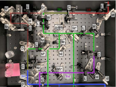
Our pump-probe CL setup integrates an SEM with an optical setup containing a femtosecond laser (Fig. 1). We use a Thermo Fisher Quanta 250 FEG SEM (), which has been modified to give optical access to the electron gun through a UV-transparent window. The femtosecond laser (Clark MXR) consists of a diode-pumped Yb-doped fiber oscillator/amplifier system, providing pulses at an output wavelength of and tunable repetition rate (-). The laser beam is directed towards an optical setup (Clark MXR) containing a set of beta barium borate (BBO) crystals to obtain the \nth2, \nth3 and \nth4 harmonics of the fundamental beam (, and , respectively). Figure 2 shows an image of the harmonic generator (HG) setup with the corresponding beam paths for the different harmonics. The HG setup is built such that we can use different combinations of two harmonics simultaneously, thus offering a large flexibility in a pump-probe experiment. For experiments requiring a larger range of excitation wavelengths, the HG setup could be replaced by an optical parametric amplifier (OPA).
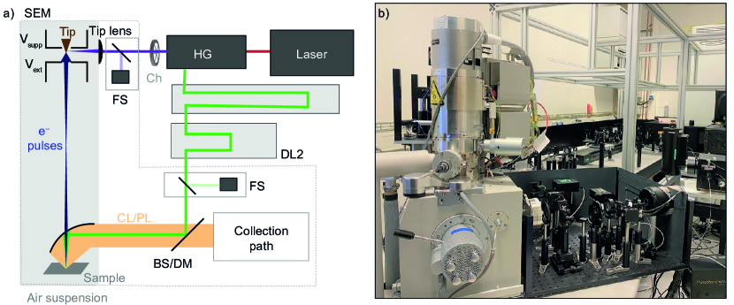
The PP setup can be divided into three main parts: generation of electron pulses, optical excitation of the sample, and collection path. The generation of electron pulses includes the focusing of one of the harmonics of the laser beam (typically the \nth4 harmonic) on the electron cathode to induce photoemission of electrons, and the subsequent path of electrons inside the microscope column. The optical excitation of the sample refers to the set of optical components designed to direct the laser beam towards the SEM chamber and focus it on the sample. Finally, the collection path denotes the set of optics and detection systems that we use to analyze the luminescence from the sample (both PL and CL).
The SEM, the collection path and part of the path to generate electron pulses are mounted on an air suspension system (see Fig. 1a), meaning that they move freely to compensate for vibrations in the room. In contrast, the rest of optical components, including the laser, is mounted on a non-floating optical table. We use two identical optical feedback systems (TEM-Messtechnik -Aligna) for the electron and light-injection paths, respectively, to actively track the movement of the floating section and move the laser beam accordingly, such that the alignment between both sections is maintained. The feedback system is composed of a position-sensitive detector (PSD) and two motorized mirror mounts. The PSD and one of the mirrors are mounted on the floating section, while the additional mirror is placed along the non-floating part (either the electron generation or the sample excitation paths). All components are connected through a controller. We use a beam sampler to send a small fraction of the laser beam to the PSD, which tracks the motion of the SEM with respect to the laser beam, and the mechanical actuators are moved accordingly to compensate for it.
We use an off-axis parabolic mirror ( focal distance, parabola coefficient a=0.1 and sr solid angle collection) positioned above the sample both to focus the laser beam on the sample and to collect the luminescence (PL or CL) [28]. The mirror has a diameter hole drilled above the focal point through which electrons pass. A motorized stage (Delmic Redux) controls the position of the mirror in the direction parallel to the sample plane. We bring the sample to the focal point of the mirror by moving the sample stage up to a working distance for the SEM of around (see section 5.1). In the next sections we will provide a detailed description of the coupling and alignment of the laser beam on the SEM gun chamber (generation of electron pulses) and chamber (optical excitation of the sample), as well as the detection and analysis of the emitted CL and PL (collection path).
3. Generation of electron pulses
The SEM is equipped with a Schottky field-emission gun (FEG), with geometry shown in Figure 1a (left). It consists of a ZrO/W electron cathode surrounded by a negatively-biased voltage usually referred to as suppressor () to ensure emission of electrons only from the apex of the tip. In normal (continuous) emission, the tip is heated up to and a positive extractor voltage () is applied to prompt emission of electrons by means of the Schottky effect. In contrast, in the PP-CL microscope we use a pulsed electron beam generated through the process of photoemission. Photoemission of electrons using a FEG source has been already reviewed in previous work [29, 4, 30]. In brief, pulsed emission of electrons is induced by focusing a fs laser beam with photon energy above the ZrO/W work function ( [31, 29]) on the electron cathode. In this case, the temperature of the cathode is lowered to to completely suppress continuous emission of electrons.
We typically use the \nth4 harmonic () of the fundamental laser beam to induce photoemission of electrons. The \nth3 harmonic of the laser beam can also be used, given that the photon energy is above the work function of the ZrO/W cathode. The beam is initally directed towards a beam expander composed of two lenses (focal length 10 and , respectively) to increase the beam size of the \nth4 harmonic beam by a factor 5. The beam is further guided up to the height of the electron cathode through a periscope. The top part of the periscope contains a dichroic mirror which reflects the \nth4 harmonic, while transmitting at longer wavelengths. Finally, the beam is focused on the electron cathode through a lens (tip lens, ) down to a spot. The position of the lens in the direction of the optical axis () is adjusted using a manually controlled linear stage, while the position in the transverse direction () is controlled by means of two motorized stages (PI M-227).
A critical step in performing time-resolved experiment with an electron microscope is the proper alignment of the laser beam on the electron cathode. The next sections show the typical procedure performed during the installation of the setup and prior to starting an experiment.
3.1. Initial alignment of the laser
The first alignment of the laser on the tip can be performed with the help of a CMOS camera and a set of irises. In normal operating conditions, the electron cathode is set to and its blackbody radiation can be observed by eye. This radiation is collected by the lens in front of the SEM window () and imaged on a CMOS camera (Thorlabs DCC1645C). In our case, we placed the CMOS camera behind the dichroic mirror from the periscope, and an achromatic lens () was used to focus the light onto the camera. A photograph of the visible blackbody radiation of the tip is shown in Fig. 3a. This configuration allows us to roughly align the lens focus on the electron cathode. The focus is later optimized by maximizing the current emitted by the cathode, as explained below. In order to align the laser on the tip (in the transverse direction, ), we placed a set of two irises through which the emitted light goes. Then the laser is aligned such that it goes through the center of the irises, thus giving a rough alignment of the laser on the tip. The exact position of the laser beam with respect to the tip is optimized by scanning the lens in front of the tip with two motorized stages, as will be explained in the next section. We should note that this initial alignment procedure is only needed during the installation of the setup or after major changes in the laser beam path.
3.2. Scanning of the lens
Once the photoemission setup is fully installed, the steps presented in the previous section can be omitted. Hence, we only need to fine-tune the position of the laser on the electron cathode within a scanning window. It is usually desirable to start the alignment of the laser beam on the tip with a hot tip, that is, using the standard settings of the electron column. When lowering the temperature of the tip, it thermally contracts by up to a few tens of [31], which results in a change of the alignment of the electron beam path inside the column. Hence, starting the alignment of the laser on the cathode with a hot tip ensures an optimum collection of the photoemitted electrons. It is also helpful to optimize the parameters inside the electron column (gun tilt/shift, condenser lens voltage and aperture) for maximum collection of the electrons in continuous mode. We collect the electron current on the sample by focusing the electron beam on a Faraday cup, placed on the sample stage, which is connected to a picoammeter (Keithley 6485) or to a lock-in amplifier (Zurich Instruments MFLI, /) through a current amplifier (Femto DLPCA-200). When the tip is hot (that is, working in continuous mode) most of the collected electron current comes from the continuous emission, even if the laser beam is already focused on the tip. However, modulating the \nth4 harmonic laser beam using an optical chopper (Hz - kHz) (Thorlabs MC2000B-EC), which is also connected to a lock-in amplifier, allows us to discern between continuous (Schottky emission) and pulsed (photoemission) electron currents. Additionally, it can be helpful to further tune the parameters inside the electron column (gun tilt/shift, condenser lens voltage and aperture) in order to maximize the collection of the photoemitted electrons.
Figure 3b shows a measurement obtained when scanning the tip lens around the electron cathode (in the plane) and collecting the electron signal from the lock-in amplifier. In this case the Schottky FEG was operating in normal conditions (, ), the electron beam acceleration was set to and the continuous (background) electron current was (using a aperture). We used a laser power () of at (/pulse). The gain of the current amplifier was set to and the chopping frequency was . We observe that photoemitted current is collected even when the laser is focused more than away from the apex of the tip. The configuration of suppressor and extractor voltage ensures that only electrons emitted from the apex of the tip can be released and go through the extractor aperture, and it is thus unlikely that electrons far from the apex (shank emission) can be efficiently released. Instead, the current observed when focusing far from the apex of tip is probably due to emission of electrons from the apex that are excited by the tail of the laser beam profile (assumed to be Gaussian).
Once the laser is aligned on the tip, we lower the temperature of the tip to suppress continuous emission. This is done by decreasing the filament current from to , resulting in a final temperature of . Figure 3c shows a scan of the tip lens obtained under the same conditions as in 3b, but at this lower temperature. Given the thermal contraction of the tip at this low temperature, here we realigned the electron column and adjusted the condenser voltage () for optimal electron collection. Here, was increased from in normal conditions to . We observe that the overall emission decreased by , down to the tens of pA range. Moreover, now emission can be observed only from a relatively small area, corresponding to the apex of the tip, due to the lower photoemission efficiency. Regardless of this reduction in the temperature of the tip, complete suppression of continuous emission is only achieved after letting the tip cool down for at least , which is not practical for experiments.
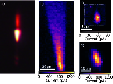
A way to instantaneously remove the remaining continuous emission is by lowering the extractor voltage, such that the effective work function of the ZrO/W tip is increased. We have observed that lowering the extractor voltage to results in the full suppression of continuous emission. Given that the photon energy of the laser beam is much larger than the work function, photoemission of electron pulses is barely affected. Further reducing the extractor voltage to results in a change in the angular spread of the photoemitted electrons, leading to a larger collection of electrons [31, 30]. In normal operating conditions, the extractor-suppressor configuration acts such that a large fraction of the emitted electrons are blocked by the extractor aperture. Instead, when the magnitude of the extractor voltage is similar to that of the suppressor, most of the emitted electrons can go though the aperture, thus increasing the collection efficiency of the photoemitted electrons [31]. We should note that this larger collection efficiency comes at the expense of spatial resolution, given that we collect electrons emitted from a larger area on the source [4, 30]. Figure 3d shows a scan of the tip lens obtained at . Given that there is not continuous emission anymore, the laser beam is not chopped and the electron current collected by the Faraday cup is sent directly to a picoammeter. Here again, the condenser lens was readjusted () together with gun tilt and shift to maximize the collection of electrons. All other parameters were kept the same as in Fig. 3c. We observe that in this case the maximum electron current is , corresponding to an average of electrons per pulse. We should note that this corresponds to one of the lowest values of the extractor voltage at which photoemission is still possible. Lowering below the magnitude of the suppressor voltage () would result in the total suppression of emission of electrons from the tip.
4. Optical excitation of the sample
In our pump-probe setup, we excite the sample with both electron and laser pulses. Hence, we need to guide one of the harmonics of the fs laser towards the sample. Here we use either the \nth2 or \nth3 harmonic beams ( and , respectively) to optically excite the sample. The \nth4 harmonic () and fundamental laser beam () could also be used to excite the sample by choosing appropriate optics. Figure 1 shows a schematic of the complete setup, in which the green line represents the laser path for sample excitation. The path is also designed to control the arrival time of the light pulses with respect to that of the electron pulses, which is essential in a pump-probe experiment. We use two free-space optical delay lines (DL1 and DL2 in the figure), consisting of a set of two mirrors (in the case of DL1) or a hollow retroreflector (Newport UBR2.5-5UV, for DL2) mounted on a mechanical stage. Moving the delay stage by corresponds to a time delay of , given the double path of the light along the stage.
The first delay line (DL1) is manually controlled and is used to coarsely adjust the zero-delay between electron and light pulses. We only align this stage at the start of an experiment, and it is kept fixed during a measurement. The operating electron energy of the SEM () determines the electron arrival time on the sample. Hence, we adjust DL1 in each experiment such that the arrival time of the laser on the sample matches the one from the electrons. For example, a electron arrives earlier to the sample than a one, which corresponds to a delay stage movement of . This delay line is also used to compensate for the different path lengths of the harmonics inside the harmonic generator, resulting in variations in their arrival time (). The physical length of DL1 is .
In a pump-probe experiment, we tune the delay between electrons and light by moving the second delay line (DL2). We use a motorized linear stage (Newport M-IMS600BPP, and motion controller Newport ESP301-1G), with total range of (), minimum step size of () and precision of (). The stage movement is controlled using a script developed for the Odemis software (Delmic), such that its movement is integrated with the acquisition of optical data. In an experiment we typically choose the center of this delay line to correspond to the zero delay between electrons and light, meaning that we can scan in a to range (with sign defined as the arrival time of the laser with respect to the electron). The temporal alignment of electron and laser beams on the sample is discussed in section 7.
After DL2, the laser beam is directed towards the SEM chamber using an 8:92 pellicle beam splitter (Thorlabs BP208) or a dichroic mirror optimized for either the \nth2 or the \nth3 harmonic (Semrock Di02-R532-25x36 and Di01-R355-25x36, respectively). The position and angle of the beam splitter or dichroic mirror is controlled by a kinematic mount and a linear stage, thus allowing us to precisely align the laser with respect to the parabolic mirror. Finally, the light is focused on the sample using the parabolic mirror described in section 2. The alignment of the laser beam on the sample is discussed in section 6.
5. Luminescence (CL/PL) collection path
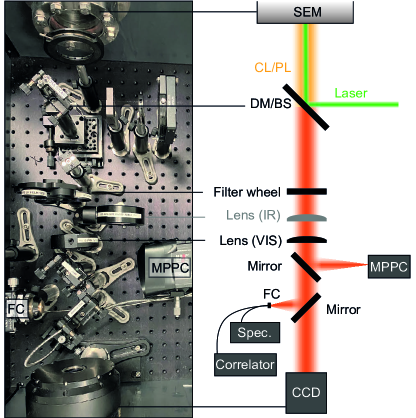
After excitation with an electron or laser beam (or both), the luminescence is collected by the parabolic mirror (described in section 2). The resulting luminescence beam is collimated and has a size determined by the mirror dimensions () [32, 33]. The luminescence is further directed outside of the SEM towards the detection path setup. A photograph of this optical setup is provided in Fig. 4, together with the corresponding schematic. We have four types of detection methods: angular, spectral, time-correlated and phase-locked. The optical components in the collection path are either on magnetic mounts or can be easily removed, such that we have full flexibility for different optical configurations, depending on the experiment. In the next sections we describe each of these detection schemes.
5.1. Alignment with CCD camera
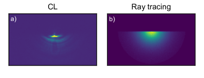
The alignment of the parabolic mirror and sample height is performed by sending the CL light directly to a 2D back-illuminated thermoelectrically-cooled CCD silicon array (PI PIXIS 1024B, 1024x1024 pixels), operating at a temperature of . In this case we do not place any additional optical components in the detection path, such that we directly collect the collimated CL beam. An example of the image obtained on the CCD for an aligned parabolic mirror and sample is provided in Figure 5a, together with a ray tracing calculation of the pattern on the CCD obtained for a point source placed at the focal point of the mirror (Fig. 5b) [34, 32].
5.2. Spectroscopy
Spectrally-resolved measurements in the visible range are performed by sending the emitted light through an achromatic lens (, ) and a silver mirror (Thorlabs PF10-03-F01) to couple it to a multimode fiber with core diameter (OZ Optics QMMJ-55-IRVIS-550/600-3AS-2). The fiber is mounted on a manually controlled 2D mechanical stage to optimize the coupling of light into the fiber in the plane perpendicular to the optical axis. The fiber guides the light to a spectrometer (PI Acton SP2300i) containing a liquid-nitrogen-cooled silicon CCD array (PI Spec-10 100F/LN, 1340x100 pixels), which reaches a temperature of for enhanced signal-to-noise ratio (SNR).
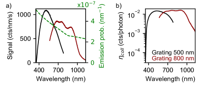
The system response of the spectral measurements is characterized by measuring the spectrum of transition radiation (TR) of a single-crystal Al sample, similar to previous works [35, 36]. Figure 6a shows TR spectra obtained upon excitation with a continuous electron beam () when using a 150 gr/nm grating with 500 and blaze (black and dark red, respectively). Fig. 6a also displays the calculated probability of photon emission per electron and wavelength bandwidth (green dashed curve), obtained using the formalism described in section IVC of ref. [37]. Using both curves we can extract the collection efficiency of our system (), defined as the number of counts detected per photon emitted by the sample. The results are shown in Fig. 6b for both gratings. The collection efficiency is not sample dependent, and can be used for any kind of CL and PL experiment, as long as we keep the same acquisition settings as in the TR measurements. Differences in the alignment of the parabolic mirror and fiber coupling can lead to changes of in the collection efficiency [35].
5.3. Time-correlated measurements
We study the dynamics of laser or electron excitation and light emission using two types of time-correlated measurements: time-correlated single-photon counting (TCSPC) and second-order autocorrelation () measurements.
Time-correlated single-photon counting
Time-correlated single-photon counting (TCSPC) measurements rely on the excitation of the sample with a pulsed beam (either electron or laser), and the subsequent analysis of the temporal statistics of the emitted light. We use the same optics (lens and mirror) as for the spectral measurements to couple the luminescence to a multimode fiber with core diameter (Thorlabs FG105UCA). The fiber is connected to an external optical setup, mounted on a portable breadboard. A photograph of the setup is shown in Fig. 7a, together with a schematic of the optical path (in orange). The luminescence is initially attenuated using a tunable neutral density filter and can be spectrally filtered with an optical filter. Next, the light goes through a set of lenses (both ) to collimate and refocus it onto a single-photon avalanche photodiode (SPAD) (PicoQuant PDM Series). The SPAD has an active area of and is mounted on a 3D mechanical stage for optimum alignment with respect to the light beam. The SPAD has a detector dead time of , thus count rates above would lead to a lower photon detection efficiency and detector damage. The entire correlator path is enclosed inside a light-tight enclosure in order to reduce background signal and protect the SPAD.
TCSPC measurements are performed by recording a histogram of the photon arrival time with respect to a reference signal (trigger), which is done using a time-correlator (PicoQuant PicoHarp 300). We direct part of the laser beam (usually the \nth2 or \nth3 harmonic) to a photodiode (PicoQuant TDA 200), which sends an electrical signal to the time-correlator, thus acting as a trigger. The time-correlator calculates the difference in arrival time between the trigger pulse and the electric pulse generated by the SPAD after detection of a CL/PL photon, thus resulting in a histogram of photon arrival time. In TCSPC measurements, only the first photon that reaches the detector from each luminescence pulse is recorded. Hence, it is important to keep a low count rate, typically of the laser rate, to avoid an overestimation of the number of photons collected in the first time bins (pile-up effect), which would lead to the recording of artificially fast dynamics [38]. To avoid this pile-up effect, the intensity of the light is controlled with a tunable neutral density filter such that, on average, less than one photon per pulse reaches the detector.
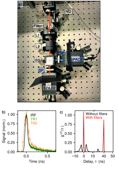
The time resolution of the TCSPC setup is determined by the instrument response function (IRF) and dispersion in the optical fiber. We measure the IRF by directly sending the \nth2 harmonic () of the fs-laser into the TCSPC setup, as shown in Fig. 7b (black curve). Considering that the laser pulse width is negligible (), we obtain an IRF of (FWHM), which is determined by the precision of the correlator, SPAD and triggering photodiode [4]. In the case of a spectrally broad luminescence signal, we also need to account for dispersion in the optical fiber. In order to quantify this effect, we measured CL time traces of transition radiation (TR) on a single-crystal Au sample using different optical filters, given that TR emission is spectrally broadband (see Fig. 6a). Fig. 7b shows traces obtained when filtering the signal in the (TR1, green) and (TR2, orange) spectral ranges. In this case we used a pulsed electron beam containing an average of and electrons per pulse (green and orange curves, respectively) ( [4, 30]). TR emission can be assumed as instantaneous ( [39]), hence the width of the time trace is determined by the IRF, dispersion of the fiber and electron pulse width ( [40, 4]). We observe that the curve obtained when filtering the luminescence in the range resembles the one for the IRF obtained with the laser, thus suggesting that both dispersion in the fiber and electron pulse width are negligible. Instead, measuring luminescence in a broader range () results in a broader time trace, which we attribute to dispersion in the optical fiber. From the measurements we estimate a dispersion of , which is reasonable for a glass-type fiber. The temporal broadening due to dispersion in the fiber could be removed by having a completely free-space coupling system.
Second-order autocorrelation () measurements
To gain further insights in laser and electron excitation dynamics, we can study the CL and PL photon correlation statistics, which are measured using second-order autocorrelation () measurements. Given a time-dependent luminescent intensity , is defined as [41]
| (1) |
where the angle brackets denote the time average. Hence, in a measurement we build a histogram of the number of coincidence events, defined as the detection of two photons, with respect to the time delay between them (). Our experiments are performed using a Hanbury Brown and Twiss geometry [42]. We use the same optical setup as for TCSPC measurements, with the difference that we now use two SPADs (1 and 2 in Fig. 7a, blue path). Both detectors are connected to the time-correlator. A 50:50 beam splitter is placed after the last lens, such that the CL/PL photons have equal probability of being detected by each SPAD. After detection of a photon by SPAD1 at a given time , the time-correlator acts as a stopwatch until a photon is detected on SPAD2 (at a time ). A count is added on the histogram at a delay corresponding to . A measurement is always symmetric, given that there is an equal probability of detecting a photon first on SPAD1 and then SPAD2 () or viceversa (). An example of a measurement is shown in Fig. 7c (dashed red), which was obtained when directing the \nth2 harmonic of the laser beam to the Hanbury Brown and Twiss setup. The curve exhibits peaks separated by the time between pulses ( at ), corresponding to correlations between photons from the same pulse (), from the next pulse () and so on [43].
A potential concern in measurements is the phenomenon of crosstalk. After detection of a photon, SPADs can emit secondary photons, typically in the infrared spectral range [44]. In measurements, the detection of this secondary photon by the second SPAD leads to the appearance of peaks at specific delays in the curve. Figure 7c (solid black) shows a measurement obtained when sending the \nth2 harmonic of the laser beam to the Hanbury Brown and Twiss setup. We observe a peak at , corresponding to the correlations between photons from the same pulse. We also observe two additional peaks separated by from the main peak, corresponding to crosstalk. Using shortpass filters allows us to filter out most of the secondary photons, thus reducing the crosstalk. Figure 7c (dashed red) shows a measurement obtained when using a shortpass filter in front of each SPAD and an additional bandpass filter () right after the fiber output. In this case, the two peaks corresponding to crosstalk are almost completely suppressed. Hence, in this setup, measurements are limited to low wavelengths ranges, below .
5.4. Lock-in detection
The previously described detection systems are based on the direct collection and analysis of the emitted light. In pump-probe measurements we have two signals: photoluminescence and cathodoluminescence, usually with very different magnitudes. This means that any spectrally or temporally-resolved measurement performed with the methods described above will be dominated by the largest signal. Hence, the analysis of the weaker signal becomes challenging, given that it can become buried in the noise of the larger signal. Moreover, in many samples CL and PL emission exhibit a similar spectrum, thus making it difficult to spectrally filter out one of those. In our PP measurements, PL is typically several orders of magnitude larger than the CL signal, partially due to the larger PL spot area compared to the CL one, as will be discussed below (section 6.1). Moreover, when using the laser as a pump, a large excitation fluence is usually needed to achieve nonlinear regimes, thus further increasing the PL/CL ratio.
A method to extract the weaker signal (here, CL) is by decreasing the measurement bandwidth, such that noise is reduced, by means of lock-in detection. In this case, we focus the luminescence (CL/PL) on a thermoelectrically-cooled multi-pixel photon counter (MPPC module, Hamamatsu C14455-3050GA, 2836 pixels). The MPPC is connected to a lock-in amplifier (Stanford Research Systems RS830 DSP). Lock-in amplifiers work as phase-sensitive detectors, which can isolate small signals modulated at a known frequency and filter out other frequency components, thus improving the signal-to-noise ratio. This allows us to separate the desired signal from noise or background signal. In our experiments, we use an optical chopper (Thorlabs MC2000B-EC) to modulate the laser beam that we use to generate electron pulses (\nth4 harmonic), typically at a few hundreds of , thus resulting in a modulated CL emission. The chopper is also connected to the lock-in amplifier and serves as a reference signal. This mechanism allows us to isolate the CL signal from a large PL background, given the difference in CL and PL modulations.
In a pump-probe measurement we usually compare the magnitude of the probe signal (either CL or PL) with and without pumping the sample (with laser or electrons, respectively). Hence, the detector (MPPC in our case) should have a low noise level so that it can detect small signals, in our case CL (), and a large dynamic range so that large PL signals do not saturate the detector, thus causing nonlinear behavior. Saturation of the MPPC during the experiment would result in artificially low signals in the pump-probe measurement compared to the reference (only CL or PL) one.
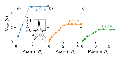
The output voltage of the MPPC as a function of incident power is shown in Figure 8 for different laser repetition rates. Here the input power is PL emission from InGaN/GaN quantum wells upon excitation with a laser beam (\nth3 harmonic). The PL spectrum is shown in the inset of Fig. 8a, and shows emission in the spectral range [36, 43]. We chose to perform the characterization using PL emission, instead of directly sending the laser towards the MPPC, to mimic the conditions of an actual pump-probe experiment. The PL power was measured using a silicon photodiode (Thorlabs S120VC) placed along the PL path. Given the lower sensitivity of the photodiode compared to the MPPC, we placed a neutral density (ND2) filter in front of the MPPC to attenuate the incoming PL. The MPPC shows a linear response up to a certain power , above which saturation is observed. The curves obtained at different repetition rates exhibit a different , ranging from at down to at . We obtain a maximum output voltage of at , very close to the expected maximum output of the MPPC (). Instead, the maximum voltage goes down to and for and , respectively. The dependence of the maximum power and output voltage on the repetition rate is attributed to the pixel recovery time. This analysis shows that in a pump-probe experiment it is crucial to ascertain that the output voltage of the signals (CL, PL and CL+PL) is sufficiently below the maximum output at the operating repetition rate.
6. Laser focusing on the sample
We use the same parabolic mirror for luminescence collection (section 2) to focus the laser beam on the sample. This configuration allows us to focus the light down to a micrometer size spot without introducing additional components in the SEM chamber. Focusing with a parabolic mirror requires a precise alignment, given that any small misalignment can lead to aberrations, thus degrading the shape of the laser spot on the sample [45, 46]. Moreover, a precise spatial overlap of electrons and light is essential in pump-probe experiments. In this section we investigate the spot size of the laser on the sample and its alignment with respect to the electron beam.
In the experiments, we align the parabolic mirror by bringing the sample into focus while optimizing the CL pattern on a CCD camera, as explained in section 5.1. This guarantees maximum collection of the CL emitted light. The laser beam is then aligned on the sample by mechanically tuning the angle of the dichroic mirror or beam-splitter (see Fig. 10a) and position it with respect to the parabolic mirror. We can also use the feedback system to precisely tune the mirror actuators, thus yielding a higher angular and spatial control.
6.1. Characterization of the laser focus
Direct imaging of the laser spot on the sample plane is challenging due to its size () and limited space in the SEM chamber. Instead, we can examine the change in secondary electron (SE) yield after optical excitation. Previous works have studied changes in SE emission in a pump-probe configuration [24, 25], from which the laser spot was imaged on the sample. For simplicity, here we rely on non-reversible changes in the SE contrast induced after repeated excitation with the laser (typically >10 s). Figure 9a shows an SE image of a -thick GaN film on a sapphire substrate (PI-KEM, undoped n-type) after exposure with the \nth3 harmonic laser beam (, average power at ). The scan was taken using a electron beam with electron current and pixel integration time. We observe a centered elongated spot with a higher SE yield, which we attribute to the laser-exposed area. This is further confirmed by tracking the movement of this spot as we misalign the laser beam with respect to the sample, as will be explained below. The mechanism behind the change in SE signal upon laser excitation is unknown. We use a laser fluence () well below the reported damage threshold of GaN under UV fs-laser excitation () [47]. Hence, it is unlikely that laser ablation plays a role. Previous studies have reported a reduction of the surface roughness of GaN upon excitation with UV ns laser pulses [48, 49], which could explain the change in SE yield. The change in SE contrast could also be due to increased contamination on the optically-excited surface, similar to the contamination typically observed in SEMs in the electron-irradiated areas [50, 51]. Further experiments with varying laser power, repetition rate and exposure time could be performed to elucidate the origin of this effect.
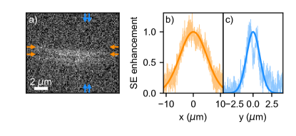
We further analyze the shape of the laser spot by taking horizontal () and vertical () cross-sections of the SE image, as shown in Fig. 9b and c, respectively. In each case, the curve is obtained by integrating over the rectangle delimited by the corresponding arrows (orange and blue in Fig. 9a). The position of this rectangle is chosen in both cases such that it yields the largest spread, thus ensuring that we characterize the largest section of the laser spot. In this experiment we ensured that the laser power was low enough to avoid any saturation effect. The solid lines represent Gaussian fits, from which we derive a laser spot size (full width at half maximum) of and in the horizontal and vertical directions, respectively. We attribute the asymmetry of the laser spot to non-perfect alignment of the laser beam with respect to the parabolic mirror.
6.2. Laser alignment on the sample
As shown above, imaging the change in SE yield after laser excitation allows us to characterize the shape and size of the laser spot on the sample. However, we have only observed this effect on specific samples and under excitation with the \nth3 harmonic laser beam. Hence, it is not practical for alignment in regular pump-probe experiments. Instead, we can align the laser beam on the sample by analyzing the image on the CCD of the PL beam, similar to the method used to align the parabolic mirror and sample height with CL (section 5.1).
We define good alignment of the laser beam as when it is centered with respect to the electron beam, that is, when it is at the focal point of the parabolic mirror. Figures 10(b-h) show various images of PL emission from GaN upon laser excitation (\nth3 harmonic beam, ), together with the corresponding SE image of the laser spot on the sample, obtained using the method discussed above. Panel (b) shows an example of satisfactory alignment of the laser. Here the CCD image resembles the one expected for a collimated beam from an off-axis parabolic mirror, as shown in Fig. 5, and we observe that the laser spot is centered with respect to the electron beam. The rest of panels in Fig. 10 show the CCD pattern and SE image for different types of misalignments of the incoming angle of the laser (polar, , and azimuthal, , angles) (c-f) and height of the sample (g, h). As a reference, a schematic of the experiment and the coordinate system is shown in Fig. 10a. The angle of the laser with respect to the parabolic mirror is tuned by controlling the tilt of the dichroic mirror (DM). We observe a clear correlation of the misalignment of the laser spot with respect to the electron beam and the pattern on the CCD. This shows that we can rely on the alignment of the laser using this technique, instead of having to image the laser spot, as in the previous section.
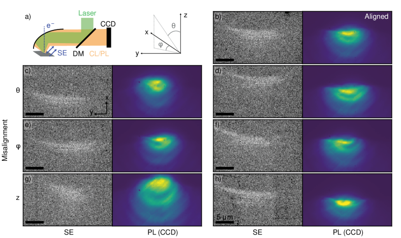
We should note that the height of the sample is fixed through the CL alignment, corresponding to the optimum collection of CL. This alignment should also correspond to best focus of the laser for a perfectly-collimated laser beam. Imperfections in the collimation can result in a focal point slightly different than the one for CL collection.
7. Temporal alignment
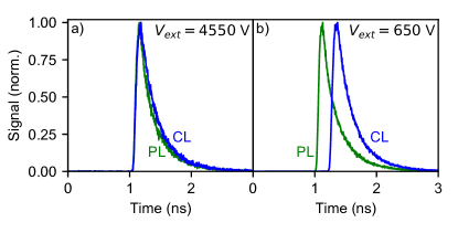
Pump-probe experiments require precise control of the timing between pump and probe (electron and laser, or vice versa). Here we describe the temporal alignment of the laser and electron pulses. We record the decay statistics of PL and CL separately using the TCSPC setup (see 5.3), from which we obtain the difference in arrival time between electron and laser pulses on the sample. Figure 11 shows decay traces of GaAs bandgap emission upon excitation with the laser beam (, ) (green curve) and electron pulses ( electrons per pulse) (blue curve). The extractor voltage at the electron gun was set to . The x-axis indicates the time at which photons are detected on the SPAD with respect to the trigger signal. The temporal overlap of both traces, shown in Fig. 11a, indicates a good time alignment between electron and laser pulses. The accuracy of this method for determining the zero-delay is limited by the minimum bin size of the time-correlator () and uncertainty in the determination of the arrival time of electrons or light from the decay curves. The latter becomes more complex when PL and CL exhibit different decay dynamics. Hence, we typically achieve an accuracy of . A higher accuracy in the determination of the zero-delay between electron and laser pulses can be obtained directly through a pump-probe experiment. In that case, the precision of the delay line stage is (see section 4), hence the temporal resolution is only limited by the electron () and laser () pulse duration, as will be discussed below.
We should note that small changes in the electron or light path directly impact the temporal alignment. As we discussed previously, changing the energy of the electrons from 5 to results in a delay of (section 4). The conditions in the photoemission of electrons, such as extractor voltage, also determine the arrival time of the electrons. Figure 11b shows decay traces of GaAs obtained under the same conditions as in (a) but at low extractor voltage (). We observe that the CL is now delayed by with respect to the PL, which is attributed to the different speed at which electrons travel along the extractor plate. Hence, a precise temporal alignment is essential before starting a pump-probe experiment. Such accurate measurements of the timing of electron arrival can give further insights in electron dynamics in both the electron source and column, both in SEM and TEM.
8. Other considerations in PP-CL experiments
The sections above describe the technical aspects in the development of a PP-CL microscope. Here, we discuss some extra considerations that need to be taken into account when designing a PP-CL experiment.
8.1. Temporal resolution
One of the main advantages of using pump-probe techniques is exploiting their high time resolution. The latter only depends on the delay between the two beams and is thus independent of the temporal precision of detectors, as happens in other time-resolved techniques. Given that typical delay stages have precision, the time resolution is typically determined by the pulse duration of one (or both) beams. In PP-CL, the duration of the electron pulse right after emission is determined by the pulse length of the laser pulse and the dynamics of the photoemission process, usually considered negligible compared to the duration of the laser pulse (hundreds of ). However, the photoemitted electrons exhibit an energy distribution, typically in the [30], which translates into a chirp, given that electrons traveling at different speeds arrive at a different time on the sample [52]. Therefore, the electron pulse duration on the sample is larger than the duration of the initial optical pulse and depends on the conditions of photoemission [30].
A way of minimizing this temporal spread of the electron pulse is by working in the regime of less than 1 electron per pulse, on average [53]. In this case, Coulomb interactions between electrons from the same pulse, and the resulting energy spread, are minimized. This approach is usually taken in other PP-type techniques using electron beams [54, 29]. However, the low electron dose used in this regime can result in a very small CL signal, in the case in which the electron is used as a probe, or low disturbance of the sample, when using the electron as a pump.
A second limitation of the pulse duration of the electron beam is given by the energy spread and electron speed in the SEM [55]. Even in the single-electron regime, electrons have an intrinsic energy spread, typically between and , determined by the conditions of the photoemission process. At this energy spread translates into a temporal spread below a the ps regime, mostly limited by the laser pulse duration. Lowering the electron energy down to results in electron pulse durations of at least , in the case of the lowest energy spread (), given the lower speed of electrons. Further information about the energy spread of electrons in an ultrafast SEM and their impact on the electron pulse duration is given in ref. [30].
8.2. Spatial resolution
A significant advantage of PP-CL measurements compared their fully optical counterparts is exploiting the high spatial resolution given by the electron beam. Similar to the temporal resolution, the best spatial resolution is achieved for beams containing a low number of electrons per pulse. In this case Coulomb repulsion, which would lead both to transverse spread and to chromatic aberrations due to the Boersch effect, is minimized [29]. Moreover, higher spatial resolutions are obtained when using emission conditions that result in a low number of photoemitted currents [4]. However, working in the regime of low number of electrons per pulse can be challenging when studying samples with low quantum efficiency.
8.3. Electron as a pump
An additional advantage of PP-CL measurements with respect to other electron-light configurations is the fact that we can now use the electron pulses as a pump, while analyzing the change in PL. Other configurations combining electron and laser pulses rely on the analysis of the electron signal, either transmitted or secondary electrons, and thus the sample is always pumped with light. An example of an experiment using the electron as a pump is given in ref. [26] when studying nitrogen-vacancy (NV) centers in diamond. Here the sample was excited with electrons and the resulting charge state of the NV centers was probed with a laser beam, showing that electron excitation induces the conversion of centers from the NV- to the NV0 state.
9. Conclusion
This paper provides a complete overview of the development of the first pump-probe cathodoluminescence microscope. We discuss the technical implementation of the setup, based on the coupling of a fs laser to the electron cathode and sample chamber of a Quanta 250 FEG SEM. We also review and characterize the different methods to analyze the luminescence emitted by the sample (either PL or CL), including spectroscopy, time-resolved and autocorrelation measurements, and lock-in based detection. Spatial alignment is performed by visualizing the laser spot on the sample, or through the analysis of the angular emission pattern of the PL light, while temporal overlap is achieved by monitoring the arrival time of electrons and light through time-resolved PL and CL measurements. Overall, this paper provides a detailed discussion and characterization of a PP-CL microscope which can be used as reference for further developments. We envision that PP-CL can be used as a new tool to understand ultrafast dynamics in materials at the nanoscale.
Acknowledgements
We gratefully acknowledge Erik Kieft (Thermo Fisher) for useful discussions and advice regarding the ultrafast SEM. We also thank Dion Ursem and Hans Zeijlemaker for their technical support and advice in the development of the PP-CL setup. This work is part of the research program of AMOLF which is partly financed by the Dutch Research Council (NWO). This project has received funding from the European Research Council (ERC) under the European Union’s Horizon 2020 research and innovation program (grant agreement No. 695343, SCEON), and the FET-Proactive program (grant agreement No. 101017720, EBEAM). S.M. acknowledges support from the French ANR funding agency through the ANR-19-CE30-0008-ECHOMELO grant.
References
- Merano et al. [2005] M. Merano, S. Sonderegger, A. Crottini, S. Collin, P. Renucci, E. Pelucchi, A. Malko, M. H. Baier, E. Kapon, B. Deveaud, and J.-D. Ganière, Probing carrier dynamics in nanostructures by picosecond cathodoluminescence. Nature 438, 479 (2005).
- Sonderegger et al. [2006] S. Sonderegger, E. Feltin, M. Merano, A. Crottini, J. F. Carlin, R. Sachot, B. Deveaud, N. Grandjean, and J. D. Ganière, High spatial resolution picosecond cathodoluminescence of InGaN quantum wells, Applied Physics Letters 89, 232109 (2006).
- Moerland et al. [2016] R. J. Moerland, I. G. C. Weppelman, M. W. H. Garming, P. Kruit, and J. P. Hoogenboom, Time-resolved cathodoluminescence microscopy with sub-nanosecond beam blanking for direct evaluation of the local density of states, Optics Express 24, 24760 (2016).
- Meuret et al. [2019] S. Meuret, M. Solà Garcia, T. Coenen, E. Kieft, H. Zeijlemaker, M. Lätzel, S. Christiansen, S. Woo, Y. Ra, Z. Mi, and A. Polman, Complementary cathodoluminescence lifetime imaging configurations in a scanning electron microscope, Ultramicroscopy 197, 28 (2019).
- Zewail [2010] A. H. Zewail, Four-Dimensional Electron Microscopy, Science 328, 187 (2010).
- Fushitani [2008] M. Fushitani, Applications of pump-probe spectroscopy, Annual Reports Section "C" (Physical Chemistry) 104, 272 (2008).
- Cabanillas-Gonzalez et al. [2011] J. Cabanillas-Gonzalez, G. Grancini, and G. Lanzani, Pump-Probe Spectroscopy in Organic Semiconductors: Monitoring Fundamental Processes of Relevance in Optoelectronics, Advanced Materials 23, 5468 (2011).
- Grumstrup et al. [2015] E. M. Grumstrup, M. M. Gabriel, E. E. Cating, E. M. Van Goethem, and J. M. Papanikolas, Pump–probe microscopy: Visualization and spectroscopy of ultrafast dynamics at the nanoscale, Chemical Physics 458, 30 (2015).
- Nakajima et al. [2008] M. Nakajima, N. Takubo, Z. Hiroi, Y. Ueda, and T. Suemoto, Photoinduced metallic state in VO2 proved by the terahertz pump-probe spectroscopy, Applied Physics Letters 92, 011907 (2008).
- Picón et al. [2016] A. Picón, C. S. Lehmann, C. Bostedt, A. Rudenko, A. Marinelli, T. Osipov, D. Rolles, N. Berrah, C. Bomme, M. Bucher, G. Doumy, B. Erk, K. R. Ferguson, T. Gorkhover, P. J. Ho, E. P. Kanter, B. Krässig, J. Krzywinski, A. A. Lutman, A. M. March, D. Moonshiram, D. Ray, L. Young, S. T. Pratt, and S. H. Southworth, Hetero-site-specific X-ray pump-probe spectroscopy for femtosecond intramolecular dynamics, Nature Communications 7, 11652 (2016).
- Murawski et al. [2015] J. Murawski, T. Graupner, P. Milde, R. Raupach, U. Zerweck-Trogisch, and L. M. Eng, Pump-probe Kelvin-probe force microscopy: Principle of operation and resolution limits, Journal of Applied Physics 118, 154302 (2015).
- Jahng et al. [2015] J. Jahng, J. Brocious, D. A. Fishman, S. Yampolsky, D. Nowak, F. Huang, V. A. Apkarian, H. K. Wickramasinghe, and E. O. Potma, Ultrafast pump-probe force microscopy with nanoscale resolution, Applied Physics Letters 106, 083113 (2015).
- Lobastov et al. [2005] V. A. Lobastov, R. Srinivasan, and A. H. Zewail, Four-dimensional ultrafast electron microscopy, Proceedings of the National Academy of Sciences 102, 7069 (2005).
- Barwick et al. [2008] B. Barwick, H. S. Park, O.-h. Kwon, J. S. Baskin, and A. H. Zewail, 4D Imaging of Transient Structures and Morphologies in Ultrafast Electron Microscopy, Science 322, 1227 (2008).
- Mohammed et al. [2011] O. F. Mohammed, D.-S. Yang, S. K. Pal, and A. H. Zewail, 4D Scanning Ultrafast Electron Microscopy: Visualization of Materials Surface Dynamics, Journal of the American Chemical Society 133, 7708 (2011).
- Barwick et al. [2009] B. Barwick, D. J. Flannigan, and A. H. Zewail, Photon-induced near-field electron microscopy, Nature 462, 902 (2009).
- García de Abajo et al. [2010] F. J. García de Abajo, A. Asenjo-Garcia, and M. Kociak, Multiphoton Absorption and Emission by Interaction of Swift Electrons with Evanescent Light Fields, Nano Letters 10, 1859 (2010).
- Feist et al. [2015] A. Feist, K. E. Echternkamp, J. Schauss, S. V. Yalunin, S. Schäfer, and C. Ropers, Quantum coherent optical phase modulation in an ultrafast transmission electron microscope, Nature 521, 200 (2015).
- Carbone et al. [2009] F. Carbone, O. H. Kwon, and A. H. Zewail, Dynamics of chemical bonding mapped by energy-resolved 4D electron microscopy, Science 325, 181 (2009).
- Schliep et al. [2017] K. B. Schliep, P. Quarterman, J.-P. Wang, and D. J. Flannigan, Picosecond Fresnel transmission electron microscopy, Applied Physics Letters 110, 222404 (2017).
- Rubiano da Silva et al. [2018] N. Rubiano da Silva, M. Möller, A. Feist, H. Ulrichs, C. Ropers, and S. Schäfer, Nanoscale Mapping of Ultrafast Magnetization Dynamics with Femtosecond Lorentz Microscopy, Physical Review X 8, 031052 (2018).
- Cremons et al. [2016] D. R. Cremons, D. A. Plemmons, and D. J. Flannigan, Femtosecond electron imaging of defect-modulated phonon dynamics, Nature Communications 7, 11230 (2016).
- Valley et al. [2016] D. T. Valley, V. E. Ferry, and D. J. Flannigan, Imaging Intra- and Interparticle Acousto-plasmonic Vibrational Dynamics with Ultrafast Electron Microscopy, Nano Letters 16, 7302 (2016).
- Liao and Najafi [2017] B. Liao and E. Najafi, Scanning ultrafast electron microscopy: A novel technique to probe photocarrier dynamics with high spatial and temporal resolutions, Materials Today Physics 2, 46 (2017).
- Garming et al. [2020] M. W. H. Garming, M. Bolhuis, S. Conesa-Boj, P. Kruit, and J. P. Hoogenboom, Lock-in Ultrafast Electron Microscopy Simultaneously Visualizes Carrier Recombination and Interface-Mediated Trapping, The Journal of Physical Chemistry Letters 11, 8880 (2020).
- Solà-Garcia et al. [2020] M. Solà-Garcia, S. Meuret, T. Coenen, and A. Polman, Electron-Induced State Conversion in Diamond NV Centers Measured with Pump–Probe Cathodoluminescence Spectroscopy, ACS Photonics 7, 232 (2020).
- Arbouet et al. [2018] A. Arbouet, G. M. Caruso, and F. Houdellier, Ultrafast Transmission Electron Microscopy: Historical Development, Instrumentation, and Applications, in Advances in Imaging and Electron Physics, Volume 207 (Elsevier, 2018) Chap. 1, pp. 1–72.
- Coenen et al. [2011] T. Coenen, E. J. R. Vesseur, and A. Polman, Angle-resolved cathodoluminescence spectroscopy, Applied Physics Letters 99, 143103 (2011).
- Feist et al. [2017] A. Feist, N. Bach, N. Rubiano da Silva, T. Danz, M. Möller, K. E. Priebe, T. Domröse, J. G. Gatzmann, S. Rost, J. Schauss, S. Strauch, R. Bormann, M. Sivis, S. Schäfer, and C. Ropers, Ultrafast transmission electron microscopy using a laser-driven field emitter: Femtosecond resolution with a high coherence electron beam, Ultramicroscopy 176, 63 (2017).
- Solà-Garcia [2021] M. Solà-Garcia, Electron-matter interaction probed with time-resolved cathodoluminescence, Ph.D. thesis, University of Amsterdam (2021).
- Bronsgeest [2009] M. Bronsgeest, Physics of Schottky electron sources, Ph.D. thesis, Delft University of Technology (2009).
- Coenen [2014] T. Coenen, Angle-resolved cathodoluminescence nanoscopy, Ph.D. thesis, University of Amsterdam (2014).
- Brenny [2016] B. J. Brenny, Probing light emission at the nanoscale with cathodoluminescence, Ph.D. thesis, University of Amsterdam (2016).
- Vesseur [2011] E. J. R. Vesseur, Electron beam imaging and spectroscopy of plasmonic nanoantenna resonances, Ph.D. thesis, Utrecht University (2011).
- Brenny et al. [2014] B. J. M. Brenny, T. Coenen, and A. Polman, Quantifying coherent and incoherent cathodoluminescence in semiconductors and metals, Journal of Applied Physics 115, 244307 (2014).
- Meuret et al. [2017] S. Meuret, T. Coenen, H. Zeijlemaker, M. Latzel, S. Christiansen, S. Conesa-Boj, and A. Polman, Photon bunching reveals single-electron cathodoluminescence excitation efficiency in InGaN quantum wells, Physical Review B 96, 035308 (2017).
- García de Abajo [2010] F. J. García de Abajo, Optical excitations in electron microscopy, Reviews of Modern Physics 82, 209 (2010).
- Wahl [2014] M. Wahl, Time-Correlated Single Photon Counting, Tech. Rep. (PicoQuant, 2014).
- Brenny et al. [2016] B. J. Brenny, A. Polman, and F. J. García De Abajo, Femtosecond plasmon and photon wave packets excited by a high-energy electron on a metal or dielectric surface, Physical Review B 94, 1 (2016).
- Sun et al. [2016] J. Sun, A. Adhikari, B. S. Shaheen, H. Yang, and O. F. Mohammed, Mapping Carrier Dynamics on Material Surfaces in Space and Time using Scanning Ultrafast Electron Microscopy, The Journal of Physical Chemistry Letters 7, 985 (2016).
- Fox [2006] M. Fox, Quantum Optics: An Introduction (Oxford University Press, 2006) p. 397.
- Hanbury Brown and Twiss [1956] R. Hanbury Brown and R. Q. Twiss, Correlation between photons in two coherent beams of light, Nature 177, 27 (1956).
- Solà-Garcia et al. [2021] M. Solà-Garcia, K. W. Mauser, M. Liebtrau, T. Coenen, S. Christiansen, S. Meuret, and A. Polman, Photon Statistics of Incoherent Cathodoluminescence with Continuous and Pulsed Electron Beams, ACS Photonics 8, 916 (2021), arXiv:2012.12375 .
- Rech et al. [2008] I. Rech, A. Ingargiola, R. Spinelli, I. Labanca, S. Marangoni, M. Ghioni, and S. Cova, Optical crosstalk in single photon avalanche diode arrays: a new complete model, Optics Express 16, 8381 (2008).
- Howard [1979] J. E. Howard, Imaging properties of off-axis parabolic mirrors, Applied Optics 18, 2714 (1979).
- Drechsler et al. [2001] A. Drechsler, M. Lieb, C. Debus, A. Meixner, and G. Tarrach, Confocal microscopy with a high numerical aperture parabolic mirror, Optics Express 9, 637 (2001).
- Eliseev et al. [1999] P. G. Eliseev, H.-B. Sun, S. Juodkazis, T. Sugahara, S. Sakai, and H. Misawa, Laser-Induced Damage Threshold and Surface Processing of GaN at 400 nm Wavelength, Japanese Journal of Applied Physics 38, L839 (1999).
- Akane et al. [1999] T. Akane, K. Sugioka, H. Ogino, H. Takai, and K. Midorikawa, KrF excimer laser induced ablation–planarization of GaN surface, Applied Surface Science 148, 133 (1999).
- Dubowski et al. [2001] J. J. Dubowski, S. Moisa, B. Komorowski, H. Tang, and J. B. Webb, Laser polishing of GaN, in Proc. SPIE 4274, Laser Applications in Microelectronic and Optoelectronic Manufacturing VI,, edited by M. C. Gower, H. Helvajian, K. Sugioka, and J. J. Dubowski (2001) pp. 442–447.
- Vladar and Postek [2005] A. Vladar and M. Postek, Electron Beam-Induced Sample Contamination in the SEM, Microscopy and Microanalysis 11, 764 (2005).
- Griffiths and Walther [2010] A. J. V. Griffiths and T. Walther, Quantification of carbon contamination under electron beam irradiation in a scanning transmission electron microscope and its suppression by plasma cleaning, Journal of Physics: Conference Series 241, 012017 (2010).
- Park et al. [2012] S. T. Park, O.-H. Kwon, and A. H. Zewail, Chirped imaging pulses in four-dimensional electron microscopy: femtosecond pulsed hole burning, New Journal of Physics 14, 053046 (2012).
- Cook and Kruit [2016] B. Cook and P. Kruit, Coulomb interactions in sharp tip pulsed photo field emitters, Applied Physics Letters 109, 151901 (2016).
- Park et al. [2007] H. S. Park, J. S. Baskin, O. H. Kwon, and A. H. Zewail, Atomic-scale imaging in real and energy space developed in ultrafast electron microscopy, Nano Letters 7, 2545 (2007).
- Gahlmann et al. [2008] A. Gahlmann, S. Tae Park, and A. H. Zewail, Ultrashort electron pulses for diffraction, crystallography and microscopy: theoretical and experimental resolutions, Physical Chemistry Chemical Physics 10, 2894 (2008).