MemPool-3D: Boosting Performance and Efficiency of Shared-L1 Memory Many-Core Clusters with
3D Integration
Abstract
Three-dimensional integrated circuits promise power, performance, and footprint gains compared to their 2D counterparts, thanks to drastic reductions in the interconnects’ length through their smaller form factor. We can leverage the potential of 3D integration by enhancing MemPool, an open-source many-core design with 256 cores and a shared pool of L1 scratchpad memory connected with a low-latency interconnect. MemPool’s baseline 2D design is severely limited by routing congestion and wire propagation delay, making the design ideal for 3D integration. In architectural terms, we increase MemPool’s scratchpad memory capacity beyond the sweet spot for 2D designs, improving performance in a common digital signal processing kernel. We propose a 3D MemPool design that leverages a smart partitioning of the memory resources across two layers to balance the size and utilization of the stacked dies. In this paper, we explore the architectural and the technology parameter spaces by analyzing the power, performance, area, and energy efficiency of MemPool instances in 2D and 3D with of scratchpad memory in a commercial technology node. We observe a performance gain of when running a matrix multiplication on the MemPool-3D design with of scratchpad memory compared to the MemPool 2D counterpart. In terms of energy efficiency, we can implement the MemPool-3D instance with of L1 memory on an energy budget smaller than its 2D counterpart, and even smaller than the MemPool-2D instance with one-fourth of the L1 scratchpad memory capacity.
Index Terms:
Many-core; 3D Integration; 3D-ICs.I Introduction
Vertical integration promises to address the scaling problems of the traditional 2D integration foreseen by Moore’s Law [1]. Three-dimensional integrated circuits (3D-ICs) promise better power, performance, and area (PPA) than 2D counterparts, thanks to a drastic reduction of the interconnect lengths, particularly of long global interconnects, while enabling a smaller form factor by adding the third dimension [2, 3].
Advances in flip-chip interconnection technology allow for the miniaturization of the inter-die connections. While controlled collapse chip connection (C4) solder bumps have a pitch of around [4], face-to-face (F2F) wafer-to-wafer hybrid bonding enables interconnect pitches in the micrometer range while maintaining reasonable yield rates [5]. Such a fine pitch can be leveraged to implement 3D-IC designs with a very high interconnect density.
For the implementation of F2F-bonded 3D-ICs, the Macro-3D flow [6] provides state-of-the-art PPA optimization capabilities for memory-on-logic partitioning schemes. Since the flow is aware of all metal layers in the die stack, the back end of the line (BEOL) routing resources of both dies can be shared [6]. It is, therefore, possible to use one chip’s BEOL to avoid congestion bottlenecks in the other chip. This resource sharing allows for a more efficient routing utilization, which is extremely useful for the implementation of highly congested designs.
Many-core systems achieve better PPA through vertical integration due to the shorter interconnect lengths. Although some many-core systems explore 3D-IC implementations [3, 7, 8], they use a 2D-mesh network to connect their processing elements, failing to exploit the interconnection capabilities of a denser pitch. In this paper, we use MemPool [9] as our target design, an open-source [10] many-core system with cores and a configurable amount of shared L1 Scratchpad Memory (SPM) connected with a low-latency interconnect. Routing congestion severely limits MemPool’s implementation, with its operating frequency bounded by the wire propagation delay. This makes MemPool an ideal candidate for 3D design. With the holistic view over all metal layers in the Macro-3D flow, the BEOL resources in both dies are combined, alleviating MemPool’s congestion and achieving a higher operating frequency thanks to reductions in the wire length. In this paper, we explore the architectural and the technology parameter spaces by analyzing the PPA impact of MemPool’s L1 SPM capacity scaling, from , on 2D and 3D implementations. The contributions of this paper are:
-
•
A flexible partitioning scheme of MemPool into logic and memory dies, capable of achieving high utilization of the memory die for large memory capacities (Section IV);
-
•
The complete 2D and Macro-3D implementations of MemPool in a commercial technology node, for all considered SPM capacities, and an analysis of the instances in terms of power, performance, area, footprint, and energy efficiency (Sections IV and V);
-
•
An exploration of MemPool’s SPM capacity and its impact on the runtime of a common matrix multiplication kernel, including an analysis of the off-chip memory bandwidth’s influence (Section VI).
II Architecture
MemPool is an open-source shared-L1 many-core cluster with very-small cores sharing a multi-banked shared-L1 SPM through a low-latency interconnect [9, 10]. Its maximum operating frequency shows a high sensibility to the available routing resources and footprint size.
II-A Tile
MemPool is built hierarchically through the replication of tiles, whose architecture can be seen in Figure 1. Each tile contains four very-small Snitch RV32IMAXpulpimg cores [11], of L1 instruction cache, and Static Random-Access Memory (SRAM) banks of SPM locally accessible within one cycle. The cores can execute instructions of the Xpulpimg extension, e.g., multiply-accumulate and load/store post-increment instructions. A fully connected logarithmic crossbar connects local cores and banks. In addition, four remote ports per tile allow remote tiles to access the local tile’s SPM banks.
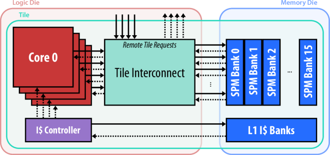
In our physical implementations with Macro-3D, the tile is partitioned into a logic and a memory die. A possible partitioning would assign all the memory banks of a tile to the memory die, namely of instruction cache and a multi-banked SPM of parameterizable capacity, as shown in Figure 1. The area requirement of per Snitch core [9] and the tile interconnect’s logic define the footprint required for the logic die. With the default SPM capacity of utilizing only of the memory die area, an increase of the SPM capacity can be used to balance the area requirement of both dies. As we will analyze in Section IV, the 3D design uses an adjusted partitioning scheme due to the increased SRAM size.
II-B Group and Cluster
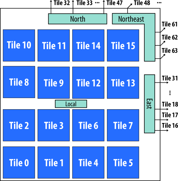
The MemPool cluster is built hierarchically using the tile as the starting point. Sixteen tiles form a group, whose architecture is shown in Figure 2. Each core can access SPM banks in the same group within three cycles. Four radix-4 butterfly networks are used in each group to connect tiles within the same group (local interconnect) or in different groups (north, northeast, and east interconnects).
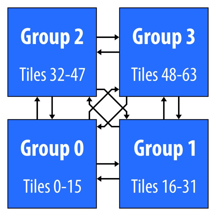
At the top level of the architecture, the MemPool cluster has four identical groups, as shown in Figure 2. Each core can access SPM banks in other groups with five cycles of latency. At this hierarchical level, there are only point-to-point connections between groups. This paper focuses on implementing the MemPool groups since only a few cells (about five thousand) need to be placed between them at the cluster level.
The dissimilarity between the tile and group makes MemPool a highly suitable architecture for 3D integration. While the tile has a high logic density, the group is highly congested due to its global interconnects. The 2D MemPool’s critical path goes from one tile to the other diagonally opposed to it. Approximately of its timing is wire propagation delay, and of its cells are buffers or inverter pairs [9].
III Methodology
MemPool is synthesized and implemented in a commercial high- technology node. In the 3D implementations, we use a fine F2F via pitch of . The F2F via size, resistance, and capacitance is , , and respectively [5]. The 3D BEOL comprises six metal layers in both tiers (M6M6), separated by the F2F via layer, similarly to the setup proposed by Bamberg et al. [6].
Tiles are first synthesized using Synopsys Design Compiler 2021.06 and then implemented with the corresponding flow in Cadence Innovus 20.13. We use a uniform frequency target on the typical corner to implement all the designs. The 2D tiles use a six-layer BEOL (M6), while the 3D tiles use the mirrored M6M6 stack mentioned above. The implemented tiles—abstracted into black boxes with full blockages on all utilized routing layers—are used for the groups’ syntheses and physical implementations, similarly to the reference flow in [9].
The 3D groups use the same BEOL as the tiles, i.e., M6M6, while the 2D groups have two extra layers (M8) to allow over-the-tile routing. When abstracting a tile implementation, the physical representation by default creates obstructions on all metal layers that are available for routing. In the 2D case, this affects M1 to M6. As the Macro-3D tile utilizes the BEOL of the logic and the memory die simultaneously, the tile abstraction blocks not only M1 to M6 of the logic die, but also M1 to M6 of the memory die. The 3D tile abstractions, therefore, prevent any inter-tile routing on the group level where tiles are placed.
In this paper, we analyze a total of eight MemPool configurations. Each configuration is named MemPool-Flow, where Capacity is the total capacity of the shared-L1 SPM at the MemPool cluster, i.e., one of , and Flow is either 2D or 3D.
IV Tile Implementation
The tiles are implemented to target a standard cell density of in the logic die. Figure 3 shows the memory die floorplanning used to implement some of the considered MemPool-3D configurations. We use the partitioning of Figure 1 to implement the tiles of the MemPool-3D configurations with of SPM. The memory die of the configuration, shown in Figure 3, only utilizes of the area of the memory die. On the other hand, the instance with of SPM, shown in Figure 3, achieves a much higher utilization, with a tile footprint only higher than the tile.
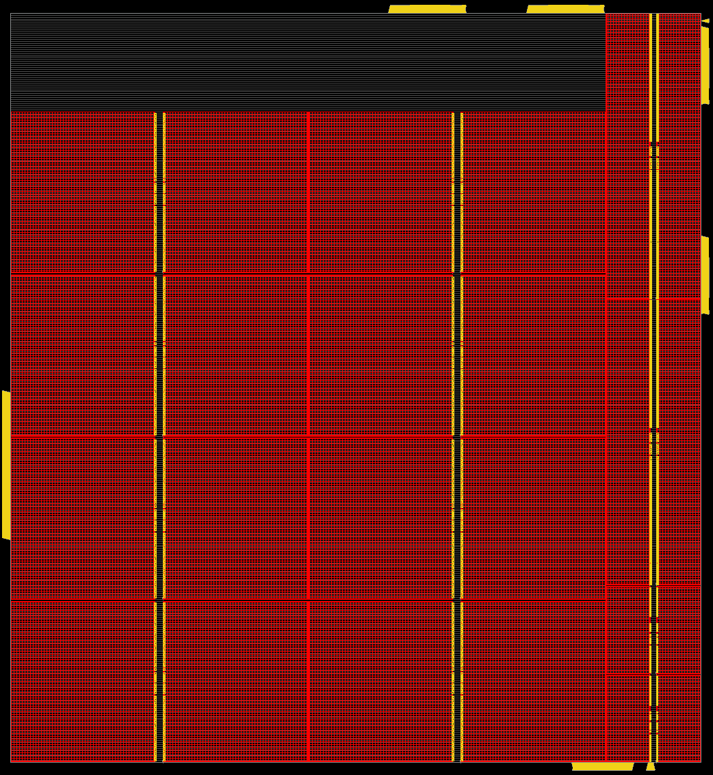
The configuration uses a partitioning different from the one shown in Figure 1 due to the increased area of the memory macros. In this configuration, out of the SPM macros are arranged in a array in the memory die. This memory die achieves near utilization, as shown in Figure 3, while its footprint is larger than the design. As we can see in Table I, both dies still keep a balanced area ratio with this partitioning. The core utilization of the logic die is , only below the target utilization. The extra area of the logic die is used by one SPM bank and all the tile’s instruction cache banks.
| Flow | SPM Capacity | Footprint | Core utilization | |
|---|---|---|---|---|
| Logic die | Memory die | |||
| 2D | — | |||
| — | ||||
| — | ||||
| — | ||||
| 3D | ||||
There is a negligible PPA difference across all tile instances. The fastest tile, , achieves a frequency only higher than the slowest tile, . This is because the tile is primarily constrained by external delays that model the group rather than internal register-to-register paths. While 3D integration can reduce the wire length of these paths, the primary effect is reducing the tile’s footprint, leading to shorter interconnects and, thus, group level PPA improvements.
V Group Implementation
V-A Area and Footprint
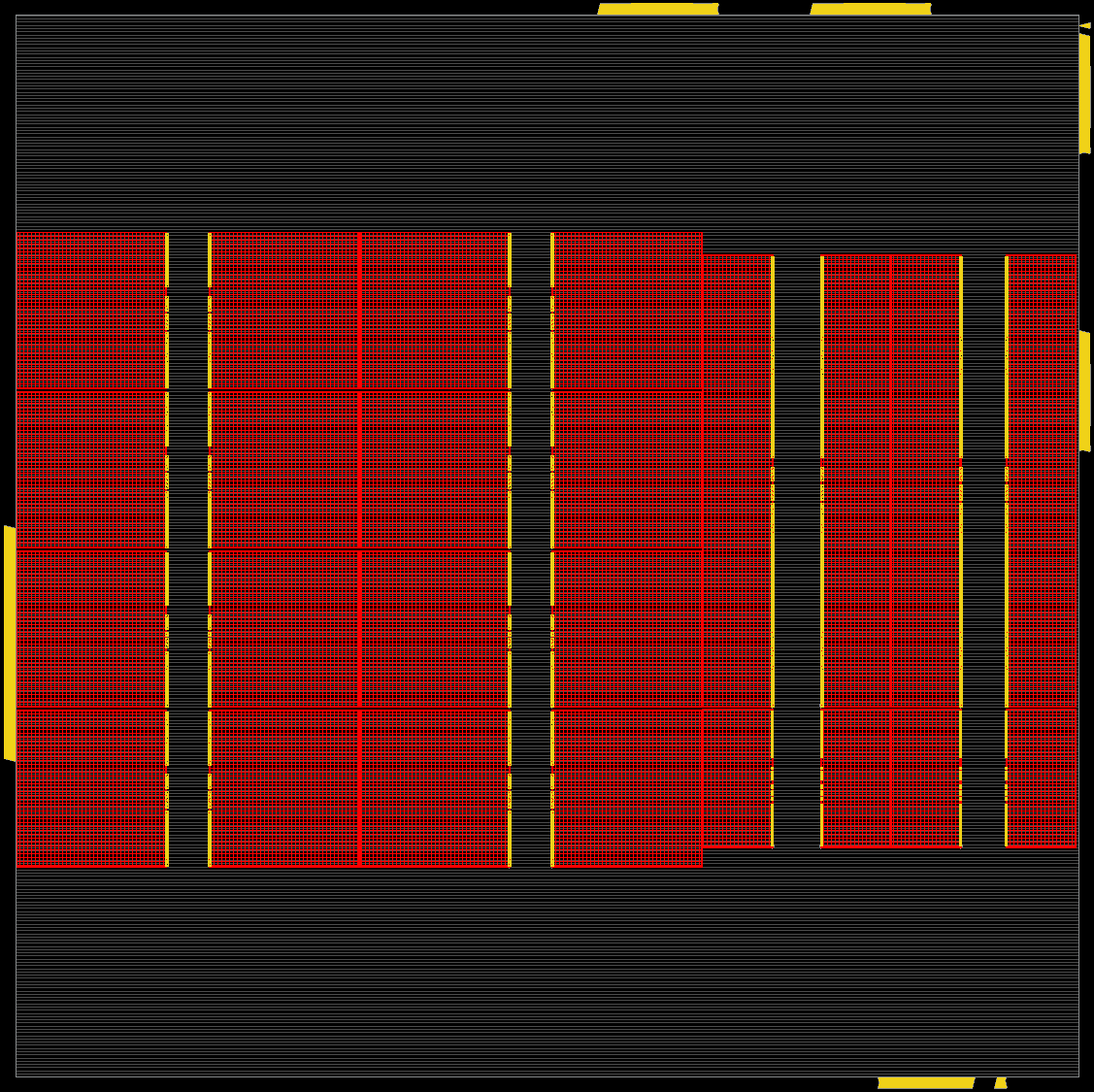
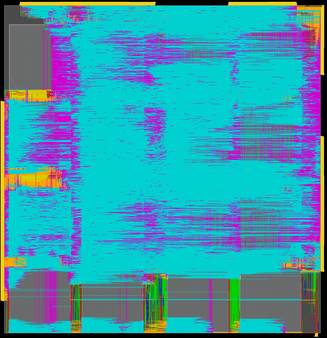
The group is at the critical level in the implementation of MemPool. When deriving the channel widths between tiles, we need to consider that the group is densely connected at the design’s center, where most of the logic of the local interconnect is placed. This causes heavy congestion, creating design rule violations (DRVs) and degrades timing if the tiles are not sufficiently spaced in the center of the design. Figure 4 exemplifies this by showing the routing and cell density map of the instance. The four group interconnects can be seen as pockets of very high cell density in Figure 4.
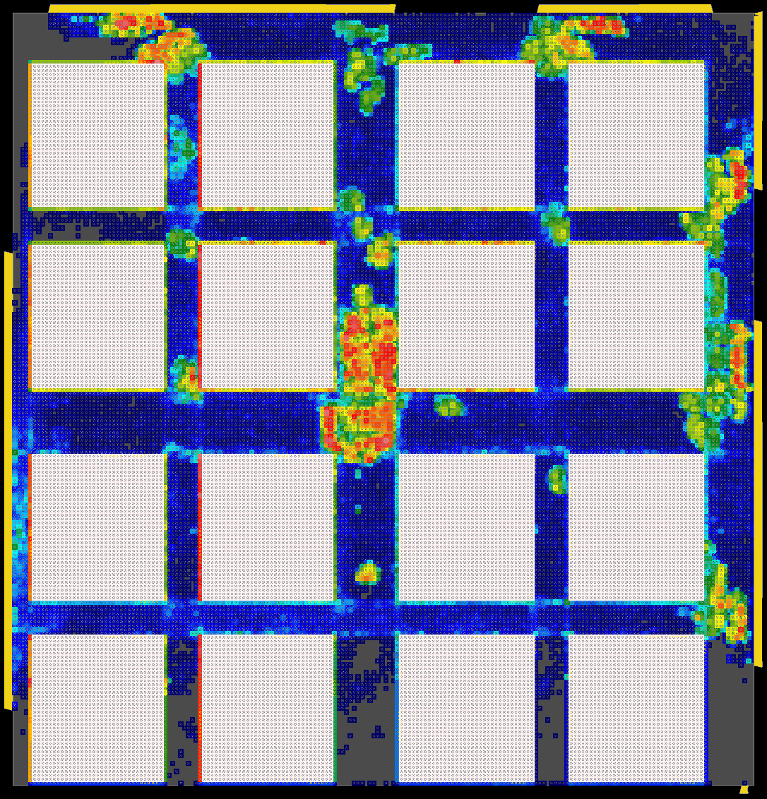
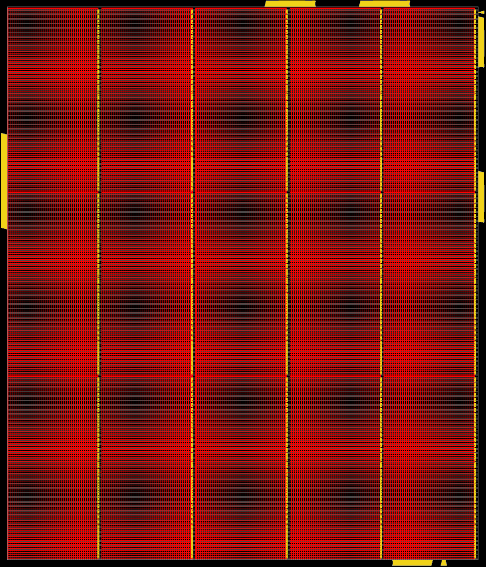
Figure 5 shows both group designs with of SPM. We highlight that the width of the channels between tiles is kept constant for all trials of each flow. The rationale is that the group interconnects’ size is largely independent of the SPM capacity, except for the additional address bits.
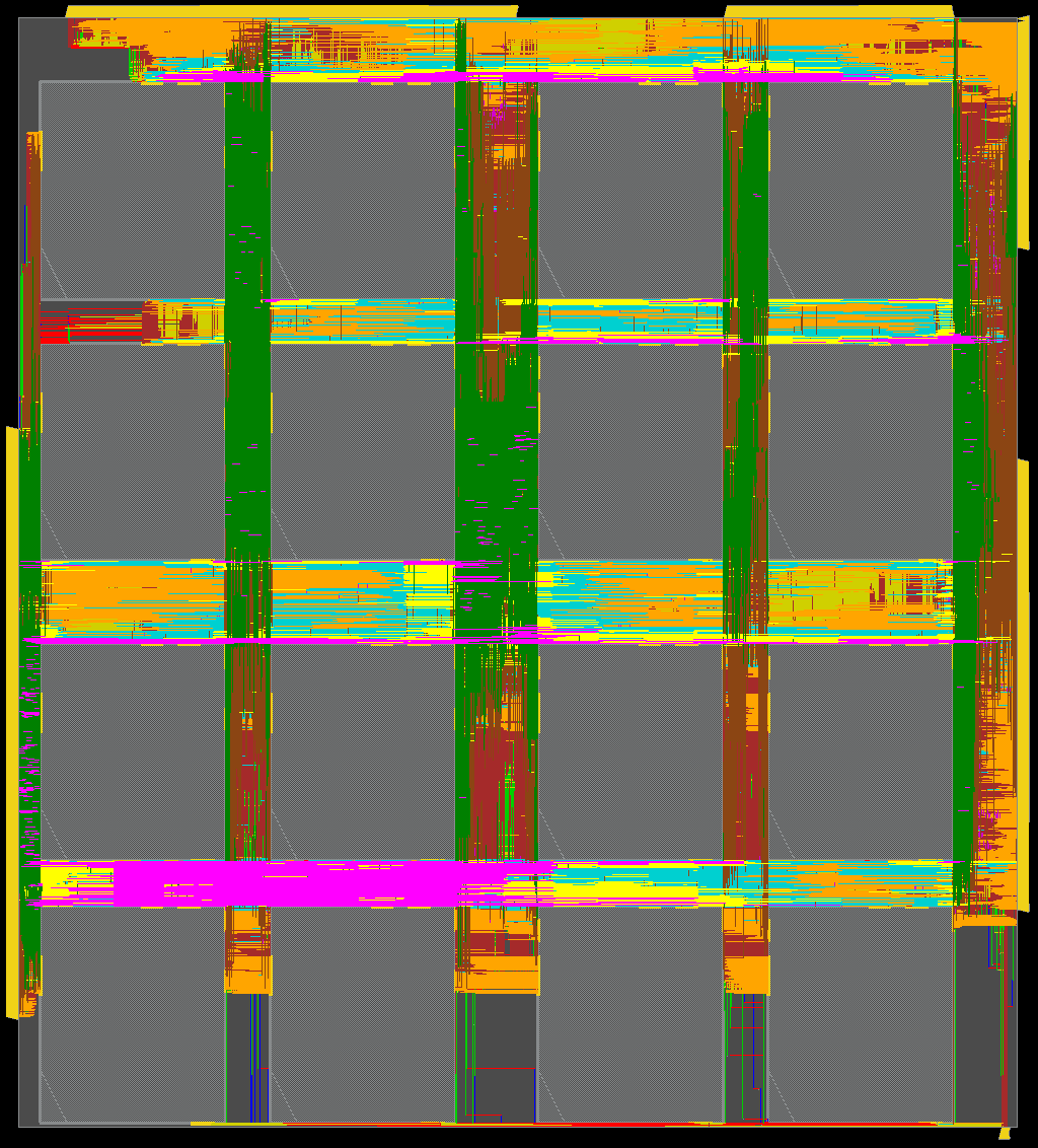
The channels between the 3D tiles are narrower than the 2D counterparts since the 3D designs have the twelve layers of the mirrored M6M6 BEOL to route the group interconnects. In contrast, the 2D trials can only use the eight layers of the M8 BEOL. This effect compounds with the reduced footprint of the 3D tiles, further reducing the footprint of the MemPool-3D groups. In Figure 5, we can also see the over-the-tile routing of the 2D designs—since the tiles are routed up to M6 and the group up to M8. Even though the 3D runs have a more aggressive BEOL than the 2D runs, M6M6, the lack of over-the-tile routing incurs extra congestion since all group interconnects have routing confined to the channels. The footprint of the MemPool-3D groups could be further reduced if routing resources of the tiles would be available to implement the group level.
Table II summarizes the implementation results of the eight considered groups, normalized by the baseline group . In terms of footprint, the 3D groups are much smaller than the 2D groups. For example, the largest 3D group, , has a footprint smaller than the smallest 2D group, . The 3D MemPool groups also have a footprint much smaller than their 2D counterparts. For instance, the group has a footprint smaller than , as seen in Figure 5.
| L1 SPM Capacity | |||||||||||
|---|---|---|---|---|---|---|---|---|---|---|---|
| Implementation Flow | 2D | 3D | 2D | 3D | 2D | 3D | 2D | 3D | |||
| BEOL | M8 | M6M6 | M8 | M6M6 | M8 | M6M6 | M8 | M6M6 | |||
| Footprint | () | () | () | () | |||||||
| Combined Die Area | () | () | () | () | |||||||
| Wire Length | |||||||||||
| Density [] | |||||||||||
| #Buffers | |||||||||||
| #F2F Bumps | — | — | — | — | |||||||
| Eff. Frequency | () | () | () | () | |||||||
| Total Negative Slack | |||||||||||
| #Failing Paths | |||||||||||
| Total Power | |||||||||||
| Power-delay product | () | () | () | () | |||||||
The combined area of the memory and logic dies of the MemPool-3D groups is larger than the area of the MemPool-2D groups. The area overhead of the MemPool-3D groups, however, decreases with increasing SPM capacity. The combined die area of the largest 3D group, , is only larger than the group area, indicating that the partitioning is closer to ideal. Although the footprint is the most important metric for analyzing PPA gains of the 3D integration thanks to reduced interconnect lengths, the combined area is more relevant for an implementation cost analysis of the 3D designs. This paper focuses on the physical implementation of the groups, MemPool’s most critical hierarchical level since the cluster only has four identical groups and some glue logic. However, it can be noted that the 12-layer mirrored BEOL of the MemPool-3D designs implies that the channels between groups needed to route the cluster-level connections can be made shorter than the equivalent channels of the MemPool-2D cluster. This means that we can expect an even more favorable area ratio at the cluster level.
V-B Power and Operating Frequency
MemPool’s sensibility to the footprint size can be seen in the normalized wire length results of Table II. The wire length of the MemPool-2D groups grows by from to , accompanied by an increase in the number of buffers. The effect compounds to other PPA metrics. For example, the 2D groups achieve an operating frequency up to slower, a power consumption up to higher, and a power-delay product (PDP) up to higher than the baseline group.
The MemPool-3D groups have a significantly smaller PPA degradation with increasing SPM capacity than the MemPool-2D groups. The low utilization of the design (Figure 3) implies it is possible to implement the group without increasing the footprint. Even the largest MemPool-3D group, with of SPM, has a footprint only larger than the group. This smaller footprint variation leads to a PPA degradation which is less drastic than the one affecting the MemPool-2D groups. As a result, the MemPool-3D groups achieve an operating frequency only slower and a power consumption only higher than the baseline group.
The benefits of 3D integration on MemPool are clearer when comparing instances with the same SPM capacity across 2D and 3D implementation flows. In general, the MemPool-3D designs have a smaller footprint, achieve a higher operating frequency, and consume less power than their 2D counterparts. In terms of footprint, the largest gains are found on the groups of the configuration, with having a footprint smaller than . In terms of frequency and PDP, the group achieves an operating frequency higher and a PDP lower than the group. It is also interesting that there is an operating frequency drop of between the and groups, despite having the same footprint. This is due to the longer SRAMs’ delay, which impacts the timing of the tile’s input-to-register and register-to-output paths. In general, the MemPool-3D groups have a higher operating frequency, consume less power, and have a lower PDP than the MemPool-2D groups with the same SPM capacity thanks to their smaller footprint and wire length.
VI Performance Analysis
We use a matrix multiplication kernel as a representative application for MemPool’s target domain to quantify the algorithmic benefits of increasing the memory capacity even for compute-bound kernels. Benefits on memory bound kernels are obviously larger, but we believe the analysis in a compute-bound regime allows us to gather more interesting insights on MemPool-3D’s performance.
VI-A Cycle count
We measure the cycle count of computing the matrix multiplication of two () matrices that do not fit into the SPM but reside in global memory through a cycle-accurate register-transfer level simulation of the luster. The matrix size is chosen to be the least common multiple of the tile sizes () that fully utilize the available SPM in each configuration, enabling optimal tiling and maximizing data reuse. The cores load the input tiles and synchronize in a memory phase before computing on the output tile in a compute phase. Those phases are repeated until the output tile is fully computed. At this point, the output tile is stored back into the main memory, and the process repeats for the subsequent output tiles. Since different output tiles require the same input data, each input element is loaded exactly times. Therefore, having a bigger SPM allows for more data reuse and less memory overhead. The second benefit of increased tile size is the increased length of the compute phase minimizing repeated static overhead due to loop setup and synchronization.
We calculate the cycle count of the memory phase for different off-chip memory bandwidths. A classic double data rate (DDR) synchronous dynamic random-access memory (SDRAM) stick has a data width of , which means a single DDR channel clocked at the same frequency as MemPool could deliver at most . Therefore, we analyze bandwidths around this realistic case, ranging from a worst-case bandwidth of to a very optimistic . Our model idealizes the latency into the off-chip global memory. We measure the duration of the compute phase with a hot instruction cache and calculate the total cycle count by accumulating all phases. The results in Figure 6 show a speedup of for the case over the baseline for the worst-case bandwidth, where the memory transfers make up a significant portion of the runtime. For the off-chip memory bandwidth of one DDR channel, the configuration with of SPM achieves a cycle count speedup of over the baseline. Even for the optimistic off-chip memory bandwidth of , the largest configuration still generates an benefit over the baseline, showing that a higher memory capacity is highly beneficial from an algorithmic point of view.
VI-B Performance and Energy-Efficiency
The increased SPM capacity impacts the PPA of the design, as seen in Section V. This Section combines those effects to analyze how MemPool’s performance and energy efficiency evolve across all considered configurations. Throughout this section, we chose an off-chip memory bandwidth of to represent our memory subsystem.
Figure 7 shows the performance of the matrix multiplication kernel on MemPool, as a function of the SPM capacity, for the MemPool-2D and MemPool-3D designs. Thanks to their higher operating frequencies, the MemPool-3D groups achieve a performance up to higher than the MemPool-2D groups. The MemPool-2D groups achieve small performance gains with increasing SPM capacity, reaching a gain of at most for the case. Due to a particularly low operating frequency, the has a performance drop compared to the design. The MemPool-3D designs, on the other hand, achieve consistently higher performances with increasing SPM capacity, outperforming their 2D counterparts. The design achieves the highest performance, above the baseline.
The energy efficiency, as expected, shows the opposite trend than the performance. As shown in Figure 8, the energy efficiency of the MemPool designs tends to decrease with an increasing SPM capacity. The group achieves the worst energy efficiency, below the efficiency of the design. In addition, the 3D designs consistently outperform their 2D counterparts. For example, the design achieves an efficiency higher than the 2D design with the same SPM capacity.
The results of Figure 8 indicate that the is the optimal design from the energy efficiency point of view, higher than . In addition, three-dimensional integration allows for the implementation of —a design with four times as much SPM capacity as the baseline design, —on an energy budget smaller. This intrinsic tradeoff between performance and energy efficiency can be better analyzed with the energy-delay product (EDP) results of Figure 9, the EDP defined as the product of the total energy consumption by the runtime. The configuration has the lowest EDP, below the baseline.
VII Conclusions
In this paper, we analyzed the power, performance, area, and energy efficiency of MemPool, through a co-exploration of its architectural and technological parameter spaces. We implemented MemPool with of SPM, using 2D and 3D implementation flows, on a modern commercial technology node.
We explored MemPool’s performance while running a large matrix multiplication kernel as a function of the L1 SPM capacity and the off-chip memory bandwidth. For a realistic bandwidth of , we observe a cycle count reduction of when increasing the SPM capacity from .
Despite the maximum operating frequency degradation with an increasing SPM capacity, the 3D designs can still achieve an operating frequency up to higher than their 2D counterparts. The design achieves a performance higher than the baseline. The 3D designs consistently outperform their 2D counterparts by up to . Regarding energy efficiency, the 3D designs outperform their 2D counterparts by up to . While increasing the SPM size in the 2D case leads to worse energy efficiency, all but the largest 3D designs achieve a better energy efficiency than the 2D baseline. We are able to implement the design with an energy budget smaller than the 2D instance with only one-fourth of the SPM capacity, . To summarize, in this paper we showed the need for a co-exploration approach with full 3D implementations to optimize modern designs constrained by their interconnect subsystems.
References
- [1] S. Panth, K. Samadi, Y. Du, and S. K. Lim, “High-density integration of functional modules using monolithic 3D-IC technology,” in 2013 18th Asia and South Pacific Design Automation Conference (ASP-DAC), 2013, pp. 681–686.
- [2] V. F. Pavlidis and E. G. Friedman, “Interconnect-based design methodologies for three-dimensional integrated circuits,” Proceedings of the IEEE, vol. 97, no. 1, pp. 123–140, 2009.
- [3] X. Dong, J. Zhao, and Y. Xie, “Fabrication cost analysis and cost-aware design space exploration for 3-D ICs,” IEEE Transactions on Computer-Aided Design of Integrated Circuits and Systems, vol. 29, no. 12, pp. 1959–1972, 2010.
- [4] W. S. Tsai, C. Y. Huang, C. K. Chung, K. H. Yu, and C. F. Lin, “Generational changes of flip chip interconnection technology,” in 2017 12th International Microsystems, Packaging, Assembly and Circuits Technology Conference (IMPACT), 2017, pp. 306–310.
- [5] E. Beyne, S.-W. Kim, L. Peng, N. Heylen, J. De Messemaeker, O. O. Okudur, A. Phommahaxay, T.-G. Kim, M. Stucchi, D. Velenis, A. Miller, and G. Beyer, “Scalable, sub µ pitch, \ceCu/SiCN to \ceCu/SiCN hybrid wafer-to-wafer bonding technology,” in 2017 IEEE International Electron Devices Meeting (IEDM), 2017, pp. 32.4.1–32.4.4.
- [6] L. Bamberg, A. García-Ortiz, L. Zhu, S. Pentapati, D. E. Shim, and S. K. Lim, “Macro-3D: A physical design methodology for face-to-face-stacked heterogeneous 3D ICs,” in 2020 Design, Automation Test in Europe Conference Exhibition (DATE), Grenoble, France, 2020, pp. 37–42.
- [7] M. B. Healy, K. Athikulwongse, R. Goel, M. M. Hossain, D. H. Kim, Y.-J. Lee, D. L. Lewis, T.-W. Lin, C. Liu, M. Jung, B. Ouellette, M. Pathak, H. Sane, G. Shen, D. H. Woo, X. Zhao, G. H. Loh, H.-H. S. Lee, and S. K. Lim, “Design and analysis of 3D-MAPS: A many-core 3D processor with stacked memory,” in IEEE Custom Integrated Circuits Conference 2010, 2010, pp. 1–4.
- [8] S. Pentapati, L. Zhu, L. Bamberg, D. E. Shim, A. García-Ortiz, and S. K. Lim, “A logic-on-memory processor-system design with monolithic 3-D technology,” IEEE Micro, vol. 39, no. 6, pp. 38–45, 2019.
- [9] M. Cavalcante, S. Riedel, A. Pullini, and L. Benini, “MemPool: A shared-L1 memory many-core cluster with a low-latency interconnect,” in 2021 Design, Automation, and Test in Europe Conference and Exhibition (DATE), Grenoble, France, Mar. 2021, pp. 701–706.
- [10] PULP Platform, “MemPool,” https://github.com/pulp-platform/mempool/, 2021, GitHub repository.
- [11] F. Zaruba, F. Schuiki, T. Hoefler, and L. Benini, “Snitch: A tiny pseudo dual-issue processor for area and energy efficient execution of floating-point intensive workloads,” IEEE Transactions on Computers, 2020.